

Page 1
LMC6953
PCI Local Bus Power Supervisor
LMC6953 PCI Local Bus Power Supervisor
April 1998
General Description
The LMC6953 is a voltage supervisory chip designed to
meet PCI (Peripheral Component Interconnect) Specifications Revision 2.1. It monitors 5V and 3.3V power supplies.
In cases of power-up, power-down, brown-out, power failure
and manual reset interrupt, the LMC6953 provides an active
low reset. RESET holds low for 100 ms after both 5V and
3.3V powers recover, or after manual reset signal returns to
high state. The external capacitor on pin 8 adjusts the reset
delay.
This part is ideal on PCI motherboards or add-in cards toensure the integrity of the entire system when there is a fault
condition. The activelowresetsetsthe microprocessor or local device in a known state.
The LMC6953 has a built-in bandgap reference that accurately determines all the threshold voltages. The internal reset delay circuitry eliminates additional discrete components.
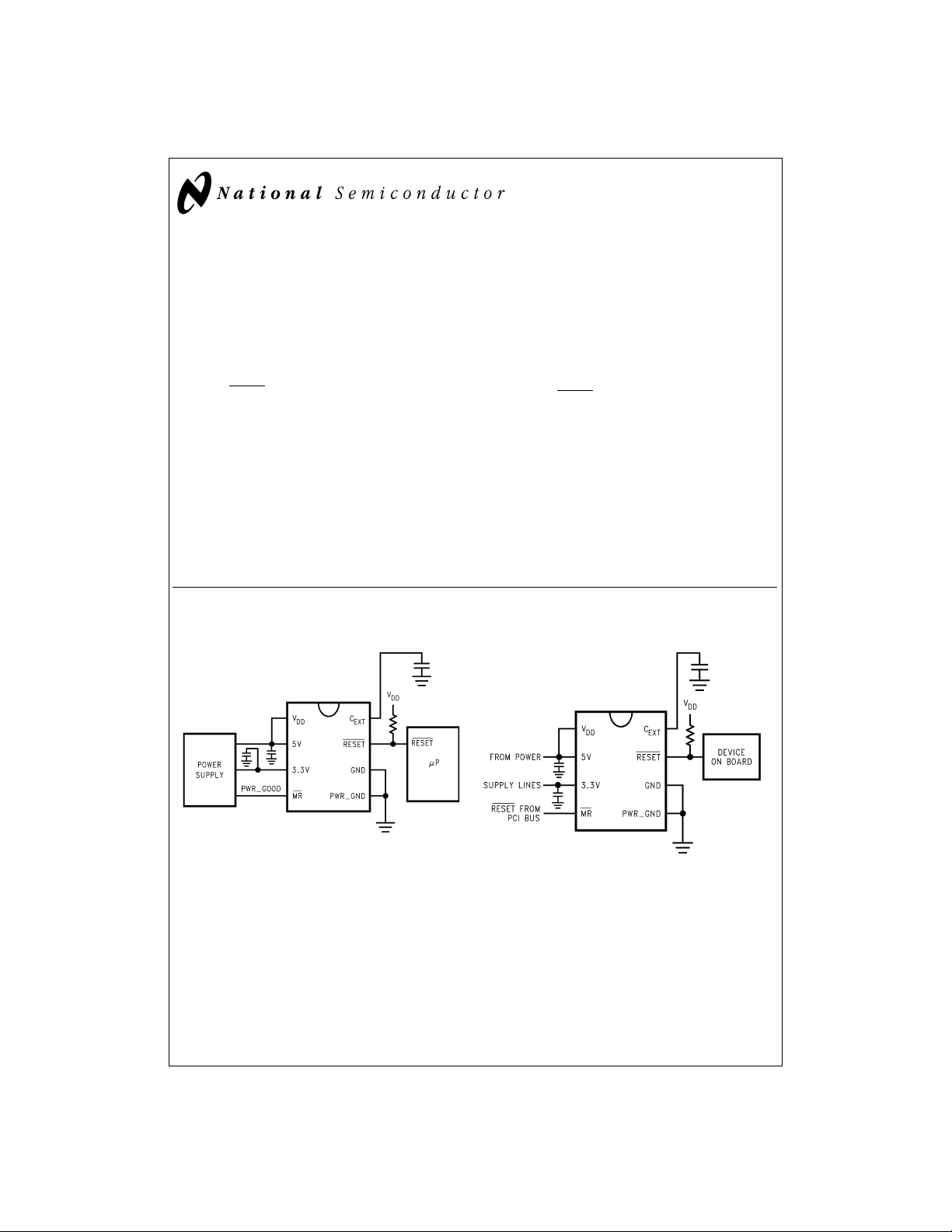
Typical Application Circuits
On Mother Board
Features
n Compliant to PCI specifications revision 2.1.
n Under and over voltage detectors for 5V and 3.3V
n Power failure detection (5V falling under 3.3V by
300 mV max)
n Manual reset input pin
n Guaranteed RESET assertion at V
n Integrated reset delay circuitry
n Open drain output
n Adjustable reset delay
n Response time for over and under voltage detection:
490 ns Max
n Power failure response time: 90 ns Max
n Requires minimal external components
=
1.5V
DD
Applications
n Desktop PCs
n PCI-Based Systems
n Network servers
On Add-in Cards
DS012846-23
DS012846-24
© 1998 National Semiconductor Corporation DS012846 www.national.com
Page 2
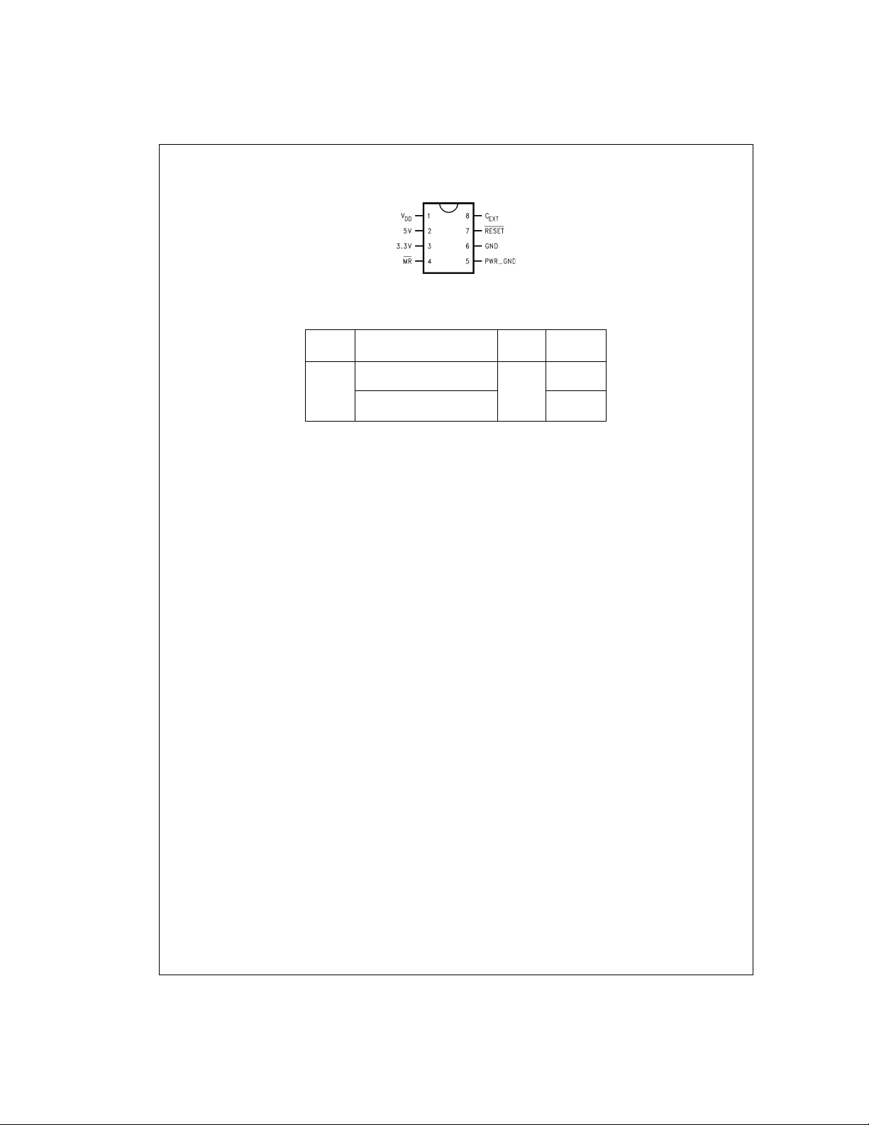
Connection Diagram
Ordering Information
Package Industrial Temp Range NSC Supplied
8-Pin
Small
Outline LMC6953CMX 2.5k Tape
8–Pin SO
DS012846-2
Top View
−40˚C to +85˚C Drawing As
LMC6953CM M08A Rails
and Reel
www.national.com 2
Page 3
Absolute Maximum Ratings (Note 1)
If Military/Aerospace specified devices are required,
please contact the National Semiconductor Sales Office/
Distributors for availability and specifications.
ESD Tolerance (Note 2)
Human Body Model 2 kV
Machine Model 200V
Voltage at Input Pin 7V
Supply Voltage 7V
Current at Output Pin 15 mA
Current at Power Supply Pin (Note 3) 10 mA
Lead Temp. (Soldering, 10 sec.) 260˚C
Storage Temperature Range −65˚C to +150˚C
Junction Temperature 150˚C
Operating Ratings (Note 1)
Supply Voltage 1.5V to 6V
Junction Temperature Range
LMC6953C −40˚C to +85˚C
Thermal Resistance (θ
M Package 165˚C/W
)
JA
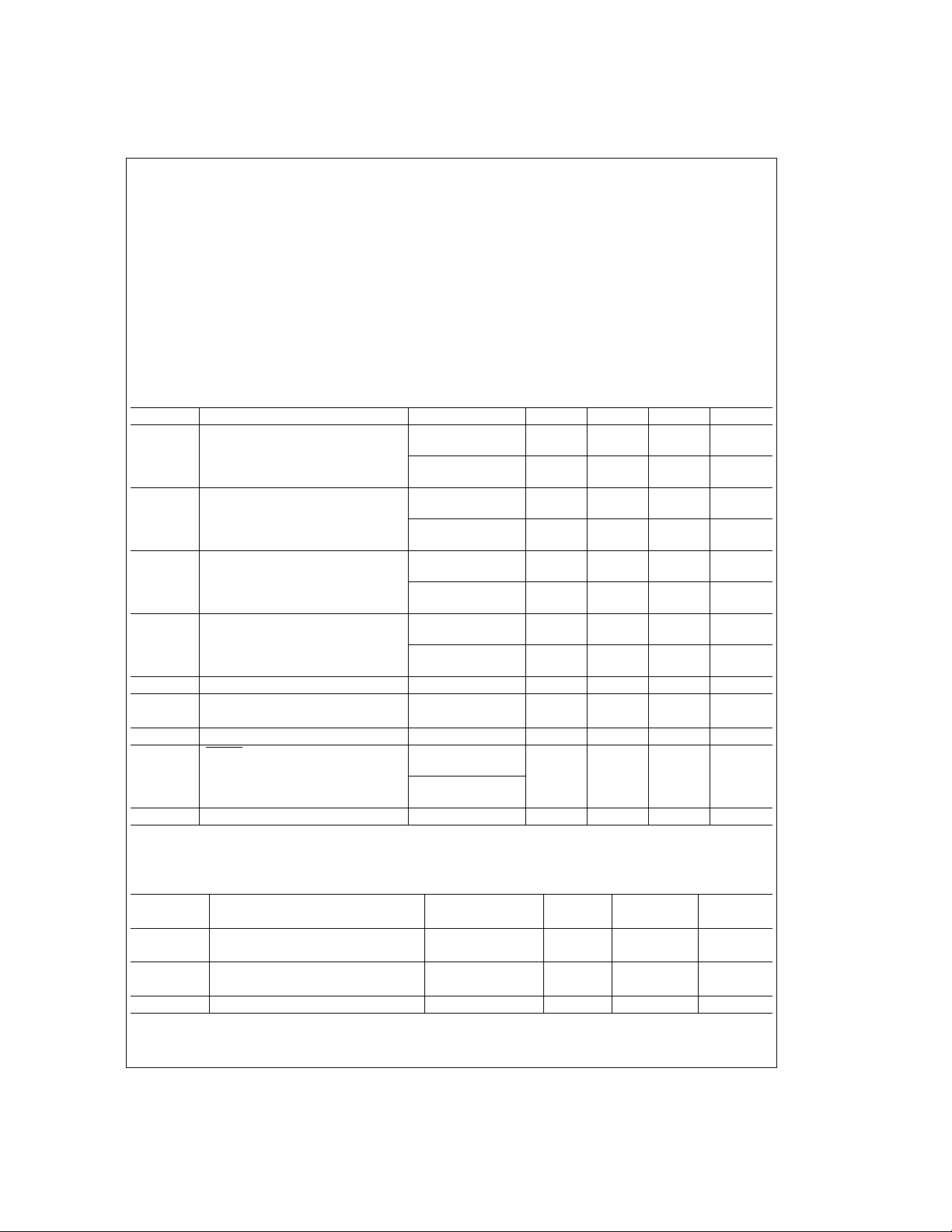
DC Electrical Characteristics
Unless otherwise specified, all boldface limits guaranteed for T
0.01 µF. Typical numbers are room temperature (25˚C) performance.
=
−40˚C to +85˚C, V
J
Symbol Parameter Conditions Min Typ Max Units
V
H5
V
L5
V
H3.3
V
L3.3
V
MR
V
PF
VDDOver-Voltage Threshold TJ= 0˚C to 70˚C
(Note 4)
T
= −40˚C to 85˚C
J
(Note 4)
VDDUnder-Voltage Threshold TJ= 0˚C to 70˚C
(Note 4)
= −40˚C to 85˚C
T
J
(Note 4)
3.3V Over-Voltage Threshold TJ= 0˚C to 70˚C
(Note 5)
= −40˚C to 85˚C
T
J
(Note 5)
3.3V Under-Voltage Threshold TJ= 0˚C to 70˚C
(Note 5)
= −40˚C to 85˚C
T
J
(Note 5)
Manual RESET Threshold 2.50 2.80 V
Power Failure Differential Voltage (Note 6) 150 300 mV
(3.3V Pin–5V Pin)
R
IN
V
OL
I
S
Input Resistance at 5V and 3.3V Pins 35 kΩ
RESET Output Low TJ= 0˚C to 70˚C
= 1.5V to 6V
V
DD
= −40˚C to 85˚C
T
J
= 1.55V to 6V
V
DD
Supply Current (Note 3) 0.8 1.50 mA
=
5V, R
DD
PULL-UP
=
4.7 kΩ and C
5.45 5.60 5.75 V
5.30 5.60 5.90 V
4.25 4.40 4.55 V
4.10 4.40 4.70 V
3.80 3.95 4.10 V
3.60 3.95 4.30 V
2.50 2.65 2.80 V
2.30 2.65 3.00 V
0.05 0.10 V
EXT
=
AC Electrical Characteristics
Unless otherwise specified, all boldface limits guaranteed for T
=
0.01 µF. Typical numbers are room temperature (25˚C) performance.
=
−40˚C to 85˚C, V
J
Symbol Parameter Conditions Typ LMC6953 Units
t
D
t
PF
t
RESET
Note 1: Absolute Maximum Ratings indicate limits beyond which damage to the device may occur. Operating Ratings indicate conditions for which the device is intended to be functional, but specific performance is not guaranteed. For guaranteed specifications and the test conditions, see the Electrical Characteristics.
Note 2: Human body model, 1.5 kΩ in series with 100 pF. Machine model. 200Ω in series with 100 pF.
Over or Under Voltage Response Time (Note 7) 150 490 ns
Power Failure Response Time (Note 8) 40 90 ns
Reset Delay C
=
0.01 µF 100 ms
EXT
3 www.national.com
=
5V, R
DD
PULL-UP
=
4.7 kΩ and C
EXT
Limit
max
max
Page 4
AC Electrical Characteristics (Continued)
Note 3: Supply current measured at pins 1, 2, and 3. The 4.7 kΩ pull-up resistor on pin 7 is not tied to VDDin this measurement.
Note 4: PCI Specifications Revision 2.1, Section 4.2.1.1 and Section 4.3.2.
Note 5: PCI Specifications Revision 2.1, Section 4.2.2.1 and Section 4.3.2.
Note 6: PCI Specifications Revision 2.1 and Section 4.3.2.
Note 7: PCISpecifications Revision 2.1, Section 4.3.2. The response time is measured individually with
drive applied to pin 3 and taking the worst number of the four measurements.
Note 8: PCI Specifications Revision 2.1, Section 4.3.2. The power failure response time is measured with a signal changing from 5V to 3V applied to pin 2 and a
3.3V DC applied to pin 3.
±
750 mV of overdrive applied to pin 2 then±600 mV of over-
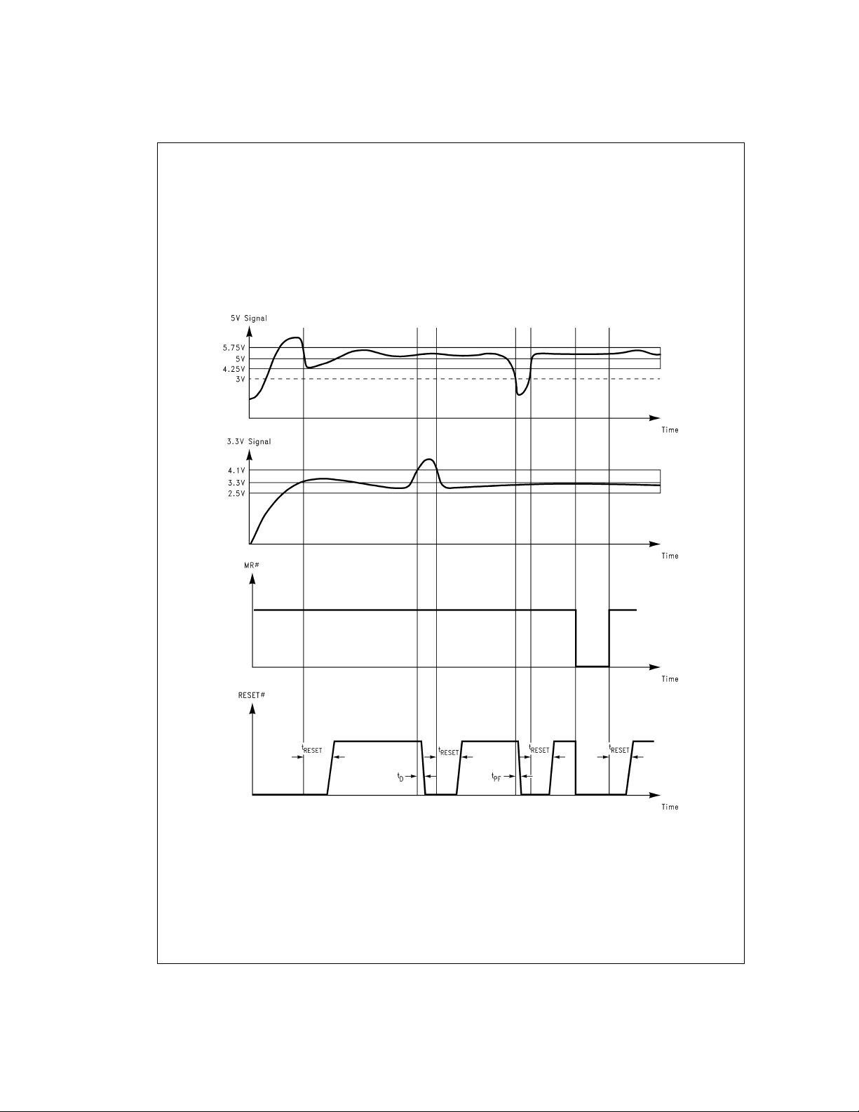
LMC6953 Timing Diagram
Note: t
www.national.com 4
and tPFare not to scale.
RESET,tD
DS012846-3
Page 5

Typical Performance Characteristics Unless otherwise specified, T
Supply Current vs Temperature
Output Voltage vs Supply Voltage
= 25˚C
A
Power-Up Supply Voltage
vs Temperature
VL5vs Temperature
DS012846-4
DS012846-9
VH5vs Temperature
V
vs Temperature
H3.3
DS012846-12
DS012846-5
DS012846-6
DS012846-7
5 www.national.com
Page 6

Typical Performance Characteristics Unless otherwise specified, T
= 25˚C (Continued)
A
vs Temperature
V
L3.3
Under-Voltage Response Time
vs Temperature
Over-Voltage Response Time
vs Temperature
DS012846-8
DS012846-13
Power Failure Response Time
vs Temperature
DS012846-14
VOLvs R
PULL-UP
DS012846-19
www.national.com 6
IOLvs R
DS012846-15
PULL-UP
DS012846-20
Page 7

Typical Performance Characteristics Unless otherwise specified, T
= 25˚C (Continued)
A
Reset Delay vs C
EXT
DS012846-10
Block Diagram of the LMC6953
Reset Delay vs Temperature
with C
EXT
=
0.01 µF
DS012846-11
**
All five comparators’ positive power supplies are connected to V
DS012846-25
DD
7 www.national.com
Page 8

Truth Table
Power
Failure
5V
Over-Voltage
5V
Under-Voltage
3.3V
Over-Voltage
3.3V
Under-Voltage
MR RESET
Fail X X X X High Low
X Fail X X X High Low
X X Fail X X High Low
X X X Fail X High Low
X X X X Fail High Low
X X X X X Low Low
OK OK OK OK OK High High
X=Don’t Care
Pin Description
Pin Name Function
1V
DD
2 5V 5V input supply voltage. This pin is not connected to the positive power supply of the
3 3.3V 3.3V input supply voltage. This pin provides input signal to the 3.3V window
4MR
5 PWR__GND Ground.
6 GND This pin should be grounded at all times.
7 RESET
8C
EXT
5V input supply voltage. This pin supplies power to the internal comparators. It can be
connected to a capacitor acting as a back-up battery. Otherwise, it should be shorted
to the 5V pin.
internal comparators. It provides input signal to the 5V window comparators as well as
the power failure comparator.
comparators and the power failure comparator.
Manual reset input pin. It takes 5V CMOS logic low and triggers RESET . If not used,
this pin should be connected to VDD.
Active low reset output. RESET holds low for 100 ms after both 5V and 3.3V powers
recover, or after manual reset signal returns to high state.
External capacitor pin. The value of C
sets the reset delay.
EXT
Application Note
HOW THE LMC6953 FUNCTIONS
The LMC6953 is a power supply supervisor with its performance specifications compliant to PCI Specifications Revision 2.1. The chip monitors power-up, power-down,
brown-out, power failure and manual reset interrupt situations.
During power-up, the LMC6953 holds RESET low for 100
ms after both 5V and 3.3V are within specified windows. It
asserts reset in 490 ns when a brown-out is detected.
Brown-out occurs when 5V supply is above 5.75V
over-voltage or below 4.25V under-voltage or when 3.3V
supply is above 4.1V over-voltage or 2.5V under-voltage. In
case of power failure where the 5V supply falls under 3.3V
supply by 300 mV maximum, reset is asserted in 90 ns. RESET also can be asserted by sending a 5V CMOS logic low
to the manual reset pin.
Each time RESET is asserted, it holds low for 100 ms after a
fault condition is recovered. The 100 ms reset delay is generated by the 0.01 µF C
by changing the value of C
It is highly recommended to place lands on printed circuit
boards for 120 pF capacitors between pin 2 and ground and
www.national.com 8
capacitor, and can be adjusted
EXT
.
EXT
also between pin 3 and ground. As power supplies may
change abruptly, there can be very high frequency noise
present and the capacitors can minimize the noise,
MINIMUM SUPPLY VOLTAGE FOR RESET ASSERTION
The LMC6953 guarantees V
supply voltage to achieve consistent RESET assertion. This
=
1.55V as the minimum
DD
ensures system stability in initialization state.
DS012846-12
FIGURE 1. Output Voltage vs Supply Voltage
Page 9

Application Note (Continued)
Figure 1
is measured by shorting pins 1, 2 and 3 together
when supply voltage is from 0V to 3.3V. Then pin 3 is connected with a constant 3.3 V
nected to a separate power supply that continues to vary
from 3.3V to 6V.
5V AND V
PINS
DD
By having the 5V and the V
be used as a back-up power supply in event of a sudden
power supply failure. This circuit is shown in the application
circuit section titled “On Motherboard With Capacitor as a
Back-up Power Supply.”Under normal condition, the diode is
forward-biased and the capacitor is charged up to V
0.7V. If the power supply goes away, the diode becomes
reverse-biased, isolating the 5V and the V
pacitor provides power to the internal comparators for a
short duration for the LMC6953 to operate.
C
SETS RESET DELAY IN LINEAR FASHION
EXT
The LMC6953 has internal delay circuitry to generate the reset delay.By choosing different values of capacitor C
set delay can be programmed to the desired length for the
system to stabilize after a fault condition occurs.
EVALUATING THE LMC6953
To Measure Over-Voltages and Under-Voltages.
Connect a 3.3V DC to the 3.3V pin and a 5V DC to the V
and the 5V pins (VDDand 5V pins are shorted). RESET output is high because voltages are within window. These voltages should be monitored. While keeping the 3.3V constant,
increase the 5V DC signal until a RESET low is detected.
The point on the 5V DC signal at which RESET changes
from high to low is the 5V over-voltage. It is typically 5.6V.To
detect 5V under-voltage, start the 5V DC signal from 5V and
decrease it until a RESET low is detected. The point on the
5V DC signal at which RESET changes from high to low is
the 5V under-voltage. It is typically 4.4V.
To find 3.3V over-voltage and under-voltage, keep the 5V
DC at 5V and vary the 3.3V DC signal until a RESET low is
detected.
To Measure Timing Specifications.
For evaluation purposes only, the V
should have separate signals. It is easier to measure response time in this manner. The V
steady 5V DC and the 5V pin is connected to a pulse generator. To simulate the power supply voltages going out of window, a pulse generator with disable/enable feature and rise
and fall time adjustment is recommended. To measure the
RESET signal, a oscilloscope is recommended because of
its ability to capture and store a signal.
To measure the 5V under-voltage response time on the
LMC6953, set the pulse generator to trigger mode and program the amplitude to have a high value of 5V and a low
value of the 5V under-voltage threshold measured previously with 50 mV overdrive. For example, if the measured 5V
under-voltage is 4.4V, then a 50 mV overdrive on this signal
is 4.35V. The disable feature on the pulse generator should
be on. Program the fall time of the pulse to be 30 ns and pro-
and pins 1 and 2 are con-
DC
pins separate, a capacitor can
DD
pins. The ca-
DD
and the 5V pins
DD
pin is connected to a
DD
EXT
DD
, re-
DD
gram the scope to trigger on the falling edge, with trigger
level of 4.5V. Set the scope to 200 ns/division. The probes
should be connected to the 5V pin and the RESET pin. Now
enable the 5V signal from the pulse generator and trigger the
signal. Be aware that when the signal is enabled, there is
high frequency noise present, and putting a 120 pF capacitor
between the 5V pin and ground suppresses some of the
noise. Response time is measured by taking the 5V
under-voltage threshold on the 5V signal to the point where
RESET goes low.
Figure 2
shows a scope photo of 5V
under-voltage waveforms. It is taken with a signal going from
5V to 4.25V at the 5V pin.
To measure the 100 ms RESET delay, change the scope to
50 ms/division and trigger the 5V signal again. RESET
−
should stay low for 100 ms after the 5V is recovered and
within window.
Other over-voltages and under-voltages can be measured
by changing the pulse generator to different voltage steps.
Putting a 120 pF capacitor between the 3.3V pin and ground
is recommended in evaluating 3.3V signal.
To measure power-failure response time, set the pulse generator from 5V to 3V with fall time of the pulse 3 ns and connect it to the 5V pin. RESET should go low within 90 ns of
power failure.
Figure 3
shows a scope photo of power failure
waveforms. It is taken with a signal going from 5V to 3V at
the 5V pin.
FIGURE 2. 5V Under-Voltage Waveforms
FIGURE 3. Power Failure Waveforms
DS012846-21
DS012846-22
9 www.national.com
Page 10

Typical Application Circuits
On Mother Board with Capacitor as a Back-up Power Supply
On Mother Board
DS012846-17
On Add-In Cards
www.national.com 10
DS012846-26
DS012846-18
Page 11

11
Page 12

Physical Dimensions inches (millimeters) unless otherwise noted
LMC6953 PCI Local Bus Power Supervisor
8-Pin Small Outline Package
Order Number LMC6953CM or LMC6953CMX
NS Package Number M08A
LIFE SUPPORT POLICY
NATIONAL’S PRODUCTS ARE NOT AUTHORIZED FOR USE AS CRITICAL COMPONENTS IN LIFE SUPPORT DEVICES OR SYSTEMS WITHOUT THE EXPRESS WRITTEN APPROVAL OF THE PRESIDENT OF NATIONAL SEMICONDUCTOR CORPORATION. As used herein:
1. Life support devices or systems are devices or systems which, (a) are intended for surgical implant into
the body, or (b) support or sustain life, and whose failure to perform when properly used in accordance
2. A critical component in any component of a life support
device or system whose failure to perform can be reasonably expected to cause the failure of the life support
device or system, or to affect its safety or effectiveness.
with instructions for use provided in the labeling, can
be reasonably expected to result in a significant injury
to the user.
National Semiconductor
Corporation
Americas
Tel: 1-800-272-9959
Fax: 1-800-737-7018
Email: support@nsc.com
www.national.com
National does not assume any responsibility for use of any circuitry described, no circuit patent licenses are implied and National reserves the right at any time without notice to change said circuitry and specifications.
National Semiconductor
Europe
Fax: +49 (0) 1 80-530 85 86
Email: europe.support@nsc.com
Deutsch Tel: +49 (0) 1 80-530 85 85
English Tel: +49 (0) 1 80-532 78 32
Français Tel: +49 (0) 1 80-532 93 58
Italiano Tel: +49 (0) 1 80-534 16 80
National Semiconductor
Asia Pacific Customer
Response Group
Tel: 65-2544466
Fax: 65-2504466
Email: sea.support@nsc.com
National Semiconductor
Japan Ltd.
Tel: 81-3-5620-6175
Fax: 81-3-5620-6179
 Loading...