

Page 1
September 1995
LMC6772
Dual Micropower Rail-To-Rail Input CMOS Comparator
with Open Drain Output
LMC6772 Dual Micropower Rail-To-Rail Input CMOS Comparator with Open Drain Output
General Description
The LMC6772 is an ultra low power dual comparator with a
maximum 10 µA/comparator power supply current. It is designed to operateover a wide range of supply voltages, with
a minimum supply voltage of 2.7V.
The common mode voltage range of the LMC6772 exceeds
both the positive and negative supply rails, a significant advantage in single supply applications. The open drain output
of the LMC6772 allows for wired-OR configurations. The
open drain output also offers the advantage of allowing the
output to be pulled to any voltage rail up to 15V, regardless
of the supply voltage of the LMC6772.
The LMC6772 is targeted for systems where low power consumption is the critical parameter. Guaranteed operation at
supply voltages of 2.7V and rail-to-rail performance makes
this comparator ideal for battery-powered applications.
Refer to theLMC6762 datasheet for a push-pull output stage
version of this device.
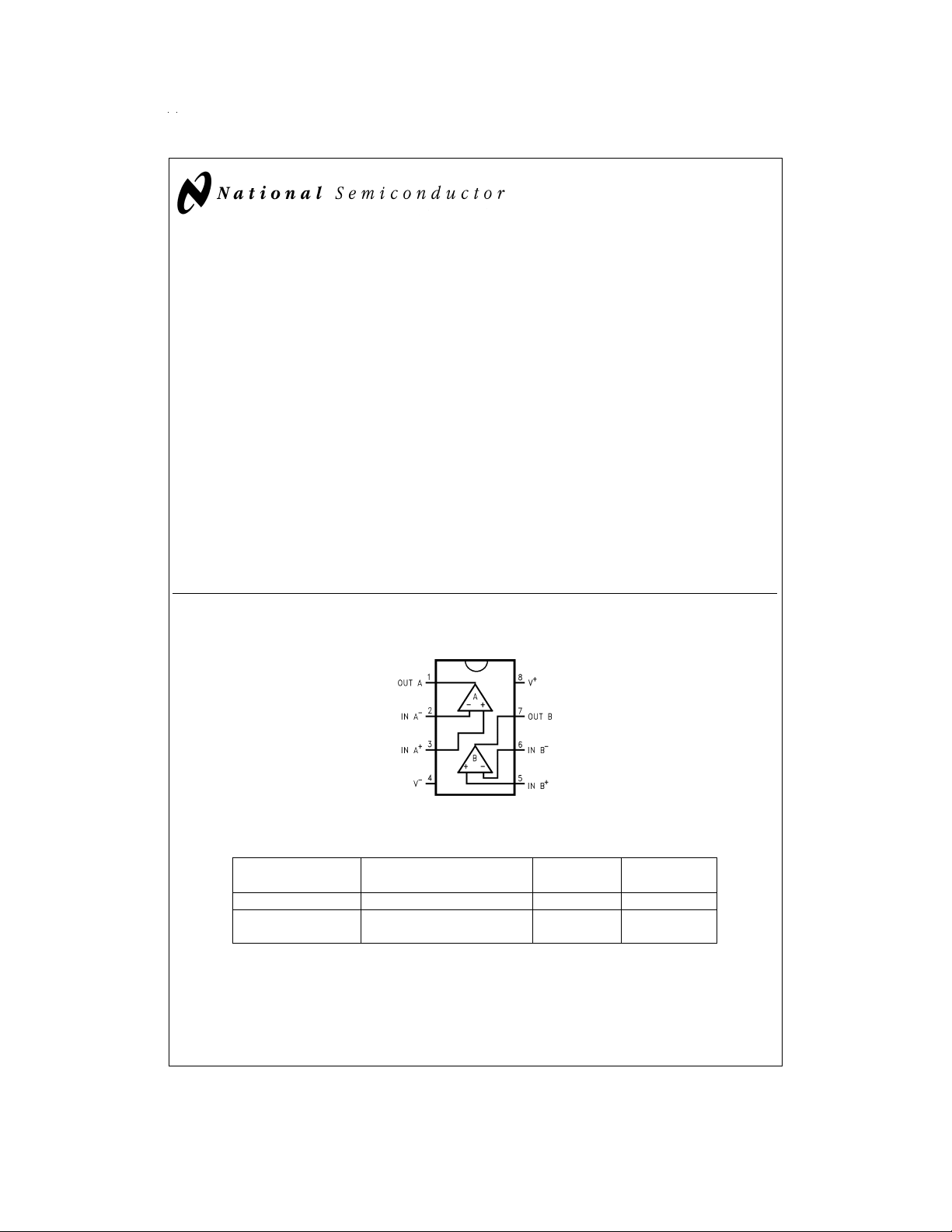
Connection Diagram
8-Pin DIP/SO
Features
(Typical unless otherwise noted)
n Low power consumption (max): I
n Wide range of supply voltages: 2.7V to 15V
n Rail-to-Rail Input Common Mode Voltage Range
n Open drain output
n Short circuit protection: 40 mA
n Propagation delay (
=
@
V
5V, 100 mV overdrive): 5 µs
S
=
10 µA/comp
S
Applications
n Laptop computers
n Mobile phones
n Metering systems
n Hand-held electronics
n RC timers
n Alarm and monitoring circuits
n Window comparators, multivibrators
DS012347-1
Top View
Ordering Information
Package Temperature Range NSC Drawing Transport
−40˚C to +85˚C Media
8-Pin Molded DIP LMC6772AIN, LMC6772BIN N08E Rails
8-Pin Small Outline LMC6772AIM, LMC6772BIM M08A Rails
LMC6772AIMX, LMC6772BIMX M08A Tape and Reel
© 1999 National Semiconductor Corporation DS012347 www.national.com
Page 2
Absolute Maximum Ratings (Note 1)
If Military/Aerospace specified devices are required,
please contact the National Semiconductor Sales Office/
Distributors for availability and specifications.
ESD Tolerance (Note 2) 1.5 kV
Differential Input Voltage (V
Voltage at Input/Output Pin (V
Supply Voltage (V
+–V−
) 16V
Current at Input Pin (Note 8)
Current at Output Pin (Notes 3, 7)
Current at Power Supply Pin, LMC6772 40 mA
Lead Temperature (Soldering, 10 seconds) 260˚C
+
)+0.3V to (V−)−0.3V
+
)+0.3V to (V−)−0.3V
±
5mA
±
30 mA
Storage Temperature Range −65˚C to +150˚C
Junction Temperature (Note 4) 150˚C
Operating Ratings (Note 1)
Supply Voltage 2.7 ≤ V
Junction Temperature Range
LMC6772AI, LMC6772BI 40˚C ≤ T
Thermal Resistance (θ
)
JA
N Package, 8-Pin Molded DIP 100˚C/W
M Package, 8-Pin Surface Mount 172˚C/W
≤ 15V
S
≤ +85˚C
J
2.7V Electrical Characteristics
Unless otherwise specified, all limits guaranteed for T
temperature extremes.
Symbol Parameter Conditions Typ
=
J
25˚C, V
+
=
2.7V, V
−
=
0V, V
(Note 5)
+
=
/2. Boldface limits apply at the
V
CM
LMC6772AI LMC6772BI Units
Limit Limit
(Note 6) (Note 6)
V
OS
Input Offset Voltage 3 5 15 mV
818max
TCV
Input Offset Voltage 2.0 µV/˚C
OS
Temperature Drift
Input Offset Voltage (Note 10) 3.3 µV/Month
Average Drift
I
B
I
OS
Input Current 0.02 pA
Input Offset Current 0.01 pA
CMRR Common Mode Rejection Ratio 75 dB
PSRR Power Supply Rejection Ratio
A
V
V
CM
Voltage Gain (By Design) 100 dB
Input Common-Mode CMRR>55 dB 3.0 2.9 2.9 V
±
1.35V<V
<
±
7.5V 80 dB
S
Voltage Range 2.7 2.7 min
−0.3 −0.2 −0.2 V
0.0 0.0 max
V
OL
Output Voltage Low I
=
2.5 mA 0.2 0.3 0.3 V
LOAD
0.4 0.4 max
I
S
Supply Current For Both Comparators 12 20 20 µA
(Output Low) 25 25 max
I
Leakage
Output Leakage Current VIN(+)=0.5V, 0.1 500 500 nA
V
(−)=0V, V
IN
=
15V
O
5.0V and 15.0V Electrical Characteristics
Unless otherwise specified, all limits guaranteed for T
apply at the temperature extremes.
Symbol Parameter Conditions Typ
V
TCV
www.national.com 2
Input Offset Voltage 3 5 15 mV
OS
Input Offset Voltage V
OS
Temperature Drift V
Input Offset Voltage V
Average Drift V
+
+
+
+
=
J
=
5V 2.0 µV/˚C
=
15V 4.0
=
5V (Note 10) 3.3 µV/Month
=
15V (Note 10) 4.0
25˚C, V
+
=
5.0V and 15.0V, V
(Note 5)
−
=
0V, V
+
=
V
CM
/2. Boldface limits
LMC6772AI LMC6772BI Units
Limit Limit
(Note 6) (Note 6)
818max
Page 3
5.0V and 15.0V Electrical Characteristics (Continued)
Unless otherwise specified, all limits guaranteed for T
apply at the temperature extremes.
=
J
Symbol Parameter Conditions Typ
I
I
CMRR Common Mode V
PSRR Power Supply Rejection Ratio
A
V
V
I
Input Current V=5V 0.04 pA
B
Input Offset Current V
OS
Rejection Ratio V
Voltage Gain (By Design) 100 dB
V
Input Common-Mode V
CM
Voltage Range CMRR
Output Voltage Low V
OL
Supply Current For Both Comparators 12 20 20 µA
S
+
=
5V 0.02 pA
+
=
5V 75 dB
+
=
15V 82 dB
±
2.5V<V
S
+
=
5.0V 5.3 5.2 5.2 V
>
55 dB 5.0 5.0 min
+
=
V
15.0V 15.3 15.2 15.2 V
>
CMRR
I
V
I
55 dB 15.0 15.0 min
+
=
5V 0.2 0.4 0.4 V
=
5mA 0.55 0.55 max
LOAD
+
=
15V 0.2 0.4 0.4 V
=
5mA 0.55 0.55 max
LOAD
(Output Low) 25 25 max
+
I
Short Circuit Current V
SC
=
15V, Sinking, V
(Note 7)
+
=
25˚C, V
5.0V and 15.0V, V
(Note 5)
<
±
5V 80 dB
−0.3 −0.2 −0.2 V
−0.3 −0.2 −0.2 V
=
12V 45 mA
O
−
=
0V, V
+
=
V
CM
/2. Boldface limits
LMC6772AI LMC6772BI Units
Limit Limit
(Note 6) (Note 6)
0.0 0.0 max
0.0 0.0 max
AC Electrical Characteristics
Unless otherwise specified, all limits guaranteed for T
the temperature extreme.
Symbol Parameter Conditions Typ
t
RISE
Rise Time f=10 kHz, C
=
J
=
50 pF, 0.3 µs
L
25˚C, V
+
=
5V, V
−
=
0V, V
(Note 5)
Overdrive=10 mV (Note 9)
t
FALL
Fall Time f=10 kHz, C
=
50 pF, 0.3 µs
L
Overdrive=10 mV (Note 9)
t
PHL
Propagation Delay f=10 kHz, 10 mV 10 µs
(High to Low) C
=
50 pF 100 mV 4 µs
L
(Note 9)
+
=
V
2.7V, 10 mV 10 µs
f=10 kHz,
=
C
50 pF 100 mV 4 µs
L
(Note 9)
+
=
=
/2. Boldface limits apply at
V
CM
V
O
LMC6772AI LMC6772BI Units
Limit Limit
(Note 6) (Note 6)
www.national.com3
Page 4
AC Electrical Characteristics (Continued)
+
Unless otherwise specified, all limits guaranteed for T
the temperature extreme.
=
J
25˚C, V
Symbol Parameter Conditions Typ
t
PLH
Propagation Delay f=10 kHz, 10 mV 10 µs
(Low to High) C
=
50 pF 100 mV 4 µs
L
=
5V, V
−
=
0V, V
(Note 5)
=
CM
(Note 9)
+
=
V
2.7V, 10 mV 8 µs
f=10 kHz,
=
C
50 pF 100 mV 4 µs
L
(Note 9)
Note 1: Absolute Maximum Ratings indicate limits beyond which damage to the device may occur. Operating Ratings indicate conditions for which the device is intended to be functional, but specific performance is not guaranteed. For guaranteed specifications and the test conditions, see the electrical characteristics.
Note 2: Human body model, 1.5 kΩ in series with 100 pF.The output pins of the two comparators (pin 1 and pin 7) have an ESD tolerance of 1.5 kV.All other pins
have an ESD tolerance of 2 kV.
Note 3: Applies to both single-supply and split-supply operation. Continuous short circuit operation at elevated ambient temperature can result in exceeding the
maximum allowed junction temperature of 150˚C. Output currents in excess of
Note 4: The maximum power dissipation is a function of T
–TA)/θJA. All numbers apply for packages soldered directly into a PC board.
Note 5: Typical Values represent the most likely parametric norm.
Note 6: All limits are guaranteed by testing or statistical analysis.
Note 7: Do not short circuit output to V
Note 8: Limiting input pin current is only necessary for input voltages that exceed absolute maximum input voltage ratings.
Note 9: C
inlcudes the probe and jig capacitance. The rise time, fall time and propagation delays are measured with a 2V input step.
L
Note 10: Input offset voltage Average Drift is calculated by dividing the accelerated operating life drift average by the equivalent operational time. The input offset
voltage average drift represents the input offset voltage change at worst-case input conditions.
+
, when V+ is>12V or reliability will be adversely affected.
, θJA, and TA. The maximum allowable power dissipation at any ambient temperature is P
J(max)
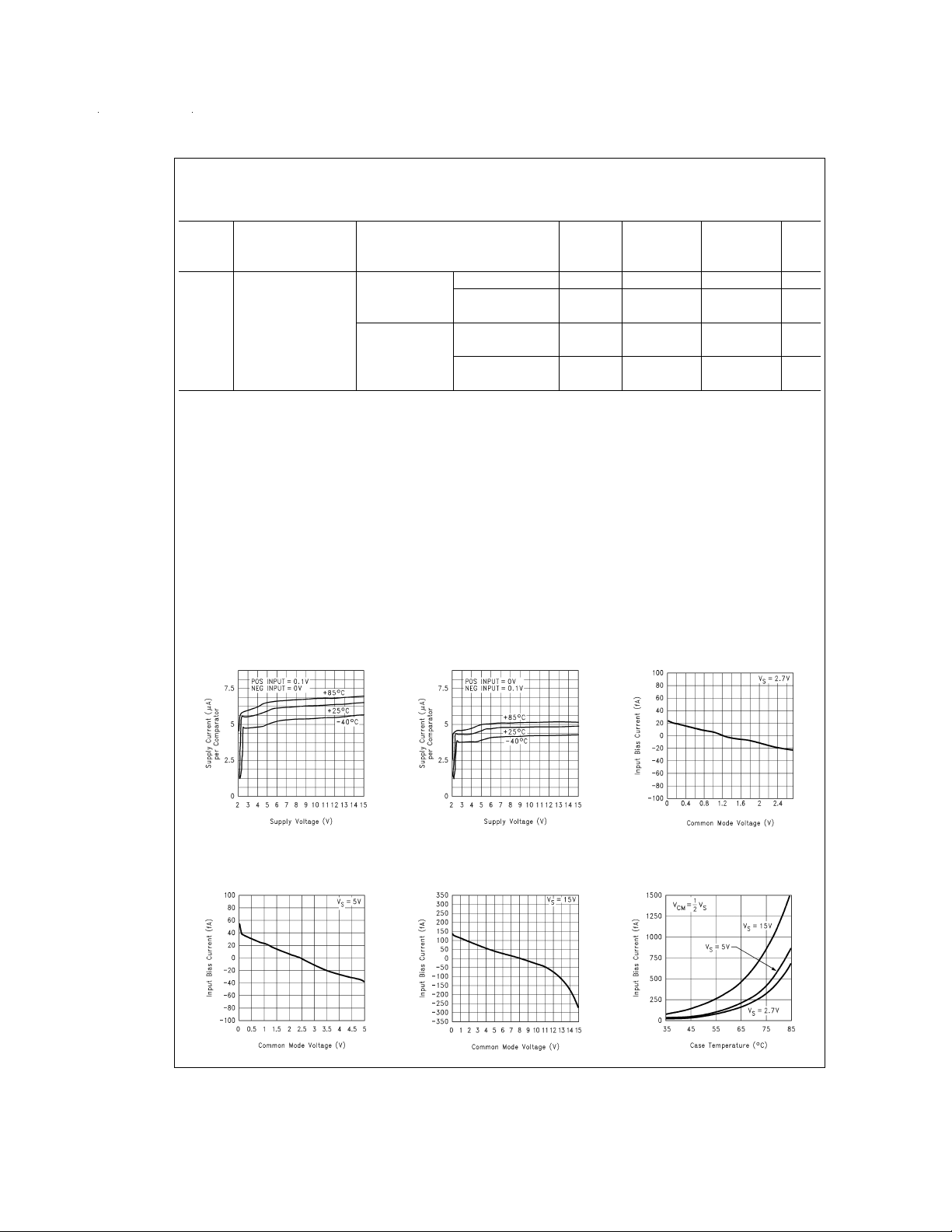
Typical Performance Characteristics V
Supply Current vs Supply
Voltage (Output High)
Supply Current vs Supply
Voltage (Output Low)
±
30 mA over long term may adversely affect reliability.
+
=
5V, Single Supply, T
+
=
/2. Boldface limits apply at
V
V
O
LMC6772AI LMC6772BI Units
Limit Limit
(Note 6) (Note 6)
=
D
=
25˚C unless otherwise specified
A
Input Current vs
Common-Mode Voltage
(T
J(max)
DS012347-3
Input Current vs
Common-Mode Voltage
DS012347-6
www.national.com 4
Input Current vs
Common-Mode Voltage
DS012347-4
DS012347-7
DS012347-5
Input Current
vs Temperature
DS012347-8
Page 5

Typical Performance Characteristics V
specified (Continued)
vs ∆V
∆V
V
OS
CM
=
2.7V
S
∆VOSvs ∆V
=
V
5V
S
CM
+
=
5V, Single Supply, T
=
25˚C unless otherwise
A
∆VOSvs ∆V
V
S
CM
=
15V
Output Voltage vs
Output Current (Sinking)
Output Short Circuit
Current (Sinking) vs
Supply Voltage
DS012347-9
DS012347-12
DS012347-15
Output Voltage vs
Output Current (Sinking)
Leakage Current
vs Output Voltage
DS012347-10
DS012347-13
DS012347-16
Output Voltage vs
Output Current (Sinking)
Response Time for
Overdrive (t
PLH
)
DS012347-11
DS012347-14
DS012347-17
www.national.com5
Page 6

Typical Performance Characteristics V
specified (Continued)
+
=
5V, Single Supply, T
=
25˚C unless otherwise
A
Response Time
for Overdrive (t
PHL
)
Response Time for
Overdrive (t
PLH
)
Application Hints
DS012347-18
DS012347-21
Response Time
for Overdrive (t
PLH
Response Time for
Overdrive (t
PHL
)
)
DS012347-19
for Overdrive (t
PHL
)
DS012347-20
Response Time vs
Capacitive Load
Response Time
DS012347-22
DS012347-23
1.0 Input Common-Mode Voltage
Range
At supply voltagesof 2.7V,5V and 15V, the LMC6772 has an
input common-mode voltage range which exceeds both supplies. As in the case of operational amplifiers, CMVR is defined by the V
common-mode range of the device. A CMRR (∆V
of 75 dB (typical) implies a shift of
common-mode range of the device. The absolute maximum
input voltage at V
at room temperature.
www.national.com 6
shift of the comparator over the
OS
<
1 mV over the entire
+
=
5V is 200 mV beyond either supply rail
OS
/∆VCM)
DS012347-24
FIGURE 1. An Input Signal Exceeds the LMC6772
Power Supply Voltages with No Output Phase
Inversion
A wide input voltage range means that the comparator can
be used to sense signals close to ground and also to the
power supplies. This is an extremely useful feature in power
supply monitoring circuits.
An input common-mode voltage range that exceeds the supplies, 20 fA input currents (typical), and a high input impedance makes the LMC6772 ideal for sensor applications. The
LMC6772 can directly interface to sensors without the use of
amplifiers or bias circuits. In circuits with sensors which produce outputs in the tens to hundreds of millivolts, the
Page 7

1.0 Input Common-Mode Voltage
Range
LMC6772 can compare the sensor signal with an appropriately small reference voltage. This reference voltage can be
close to ground or the positive supply rail.
(Continued)
2.0 Low Voltage Operation
Comparators are the common devices by which analog signals interface with digital circuits. The LMC6772 has been
designed to operate at supply voltages of 2.7V, without sacrificing performance, to meet the demands of 3V digital systems.
At supply voltages of 2.7V,the common-mode voltage range
extends 200 mV (guaranteed) below the negative supply.
This feature, in addition to the comparator being able to
sense signals nearthe positive rail, is extremely useful in low
voltage applications.
DS012347-26
FIGURE 3. Canceling the Effect of Input Capacitance
The capacitor added across the feedback resistor increases
the switching speed and provides more short term hysteresis. This can result in greater noise immunity for the circuit.
5.0 Spice Macromodel
A Spice Macromodel is available for the LMC6772. The
model includes a simulation of:
Input common-mode voltage range
•
Quiescent and dynamic supply current
•
Input overdrive characteristics
•
and many more characteristics as listed on the macromodel
disk.
Contact the National Semiconductor Customer Response
Center at 1-800-272-9959 to obtain an operational amplifier
spice model library disk.
Typical Applications
DS012347-25
FIGURE 2. Even at Low-Supply Voltage of 2.7V, an
Input Signal which Exceeds the Supply Voltages
Produces No Phase Inversion at the Output
+
=
At V
2.7V,propagation delays are t
4 µs with overdrives of 100 mV. Please refer to the performance curves for more extensive characterization.
PLH
=
4 µs and t
PHL
3.0 Output Short Circuit Current
The LMC6772 has short circuit protection of 40 mA. However,it is not designed to withstand continuous short circuits,
transient voltage or current spikes, or shorts to any voltage
beyond the supplies. A resistor is series with the output
should reduce the effect of shorts. For outputs which send
signals off PC boards additional protection devices, such as
diodes to the supply rails, and varistors may be used.
4.0 Hysteresis
If the input signal is very noisy, the comparator output might
trip several times as the input signal repeatedly passes
through the threshold. This problem can be addressed by
making use of hysteresis as shown below.
Universal Logic Level Shifter
The output of the LMC6772 is the uncommitted drain of the
output NMOS transistor. Many drains can be tied together to
provide an output OR’ing function. An output pullup resistor
can be connected to any available power supply voltage
=
within the permitted power supply range.
FIGURE 4. Universal Logic Level Shifter
The two 1 kΩ resistors bias the input to half of the power
supply voltage. The pull-up resistor should go to the output
logic supply. Due to its wide operating range, the LMC6772
is ideal for the logic level shifting applications.
DS012347-27
www.national.com7
Page 8

Typical Applications (Continued)
One-Shot Multivibrator
DS012347-28
FIGURE 5. One-Shot Multivibrator
A monostable multivibrator has one stable state in which it
can remain indefinitely. It can be triggered externally to another quasi-stable state.Amonostable multivibrator can thus
be used to generate a pulse of desired width.
The desired pulse width is set by adjusting the values of C
and R4. The resistor divider of R1and R2can be used to determine the magnitude of the input trigger pulse. The
LMC6772 will change state when V
vides a rapid discharge path for capacitor C
end of the pulse. The diode also prevents the non-inverting
input from being driven below ground.
Bi-Stable Multivibrator
<
V2. Diode D2pro-
1
to reset at the
2
Zero Crossing Detector
FIGURE 7. Zero Crossing Detector
A voltage divider of R
age V
at the non-inverting input. By making the series resis-
1
tance of R
2
when V
−0.7V. The voltage divider of R
and R2equal to R5, the comparator will switch
1
=
0. Diode D
IN
from going below ground. A small amount of hysteresis is
and R5establishes a reference volt-
4
insures that V3never drops below
1
and R3then prevents V
2
setup to ensure rapid output voltage transitions.
Oscillator
DS012347-29
2
DS012347-30
FIGURE 6. Bi-Stable Multivibrator
Abi-stable multivibrator has two stable states. The reference
voltage is set up by the voltage divider of R
applied to the SET terminal will switch the output of the comparator high. The resistor divider of R
clamps the non-inverting input to a voltage greater than the
and R3. A pulse
2
, and R5now
1,R4
reference voltage.A pulse applied to RESET will now toggle
the output low.
www.national.com 8
DS012347-31
FIGURE 8. Square Wave Generator
Figure 8
shows the application of the LMC6772 in a square
wave generator circuit. The total hysteresis of the loop is set
by R
discharge paths for the capacitor C. The charge path is set
through R
the RC time constant of R
path for the capacitor is set by R
between the pulses can be changed by varying R5, and the
pulse width can be altered by R
put can be changed by varying both R
and R3.R4and R5provide separate charge and
1,R2
and D1. So, the pulse width t1is determined by
4
and C. Similarly, the discharge
4
and D2. Thus, the time t
5
. The frequency of the out-
4
and R5.
4
2
Page 9

Typical Applications (Continued)
Time Delay Generator
FIGURE 9. Time Delay Generator
The circuit shown above provides output signals at a prescribed time interval from a time reference and automatically
resets the output when the input returns to ground. Consider
the case of V
ground. This implies that the outputs of comparators 1, 2,
=
0. The output of comparator 4 is also at
IN
and 3 are also at ground. When an input signal is applied,
the output of comparator 4 swings high and C charges expo-
DS012347-32
nentially through R. This is indicated above. The output voltages of comparators 1, 2, and 3 swtich to the high state
when V
A small amount of hysteresis has been provided to insure
rises above the reference voltages VA,VBand VC.
C1
fast switching when the RC time constant is chosen to give
long delay times.
www.national.com9
Page 10

Physical Dimensions inches (millimeters) unless otherwise noted
8-Pin Small Outline Package
Order Number LMC6772AI or LMC6772BI
NS Package Number M08A
8-Pin Molded Dual-In-Line Package
Order Number LMC6772AI or LMC6772BI
NS Package Number N08E
www.national.com 10
Page 11

Notes
LMC6772 Dual Micropower Rail-To-Rail Input CMOS Comparator with Open Drain Output
LIFE SUPPORT POLICY
NATIONAL’S PRODUCTS ARE NOT AUTHORIZED FOR USE AS CRITICAL COMPONENTS IN LIFE SUPPORT
DEVICES OR SYSTEMS WITHOUT THE EXPRESS WRITTEN APPROVAL OF THE PRESIDENT OF NATIONAL
SEMICONDUCTOR CORPORATION. As used herein:
1. Life support devices or systems are devices or
systems which, (a) are intended for surgical implant
into the body, or (b) support or sustain life, and
whose failure to perform when properly used in
accordance with instructions for use provided in the
2. A critical component is any component of a life
support device or system whose failure to perform
can be reasonably expected to cause the failure of
the life support device or system, or to affect its
safety or effectiveness.
labeling, can be reasonably expected to result in a
significant injury to the user.
National Semiconductor
Corporation
Americas
Tel: 1-800-272-9959
Fax: 1-800-737-7018
Email: support@nsc.com
www.national.com
National does not assume any responsibility for use of any circuitry described, no circuit patent licenses are implied and National reserves the right at any time without notice to change said circuitry and specifications.
National Semiconductor
Europe
Fax: +49 (0) 1 80-530 85 86
Email: europe.support@nsc.com
Deutsch Tel: +49 (0) 1 80-530 85 85
English Tel: +49 (0) 1 80-532 78 32
Français Tel: +49 (0) 1 80-532 93 58
Italiano Tel: +49 (0) 1 80-534 16 80
National Semiconductor
Asia Pacific Customer
Response Group
Tel: 65-2544466
Fax: 65-2504466
Email: sea.support@nsc.com
National Semiconductor
Japan Ltd.
Tel: 81-3-5639-7560
Fax: 81-3-5639-7507
 Loading...