

Page 1
LMC6681 Single/LMC6682 Dual/LMC6684 Quad
Low Voltage, Rail-To-Rail Input and Output CMOS
Amplifier with Powerdown
General Description
The LMC6681/2/4 is a high performance operational amplifier which can operate over a wide range of supply voltages,
with guaranteed specifications at 1.8V, 2.2V, 3V, 5V, and
10V.
The LMC6681/2/4 provides an input common-mode voltage
range that exceeds both supplies. The rail-to-rail output
swing of the amplifier assures maximum dynamic signal
range. This rail-to-rail performance of the amplifier, combined with its high open-loop voltage gain makes it unique
among CMOS rail-to-rail amplifiers. The LMC6681/2/4 is an
excellent choice for circuits where the common-mode voltage range is a concern.
The LMC6681/2/4 has a powerdown mode which can be
controlled externally. In this powerdown mode, the supply
current decreases from 700 µA per amplifier to less than 1
µA per amplifier. The LMC6684 has two powerdown options.
Each of the powerdown pins disables two amplifiers.
The LMC6681/2/4 has been designed specifically to improve
system performance in low voltage applications. The amplifier’s 80 fA input current, 0.5 mV offset voltage, and 82 dB
CMRR maintain accuracy in battery-powered systems.
Features
(Typical unless otherwise noted)
n Guaranteed Specs at 1.8V, 2.2V, 3V, 5V, 10V
n Rail-to-Rail Input Common-Mode Voltage Range
n Rail-to-Rail Output Swing
(within 10 mV of supply rail,
@
V
S
=
3V and R
L
=
10 kΩ)
n Powerdown Mode I
S OFF
≤ 1.5 µA/Amplifier
(Guaranteed at V
S
=
1.8V, 2.2V, 3V, and 5V)
n Ultra Low Input Current 80 fA
n High Voltage Gain (V
S
=
3V, R
L
=
10 kΩ): 120 dB
n Unity Gain Bandwidth 1.2 MHz
Applications
n Battery Operated Circuits
n Sensor Amplifiers
n Portable Communication Devices
n Medical Instrumentation
n Battery Monitoring Circuits
n Level Detectors, Sample-and-Hold Circuits
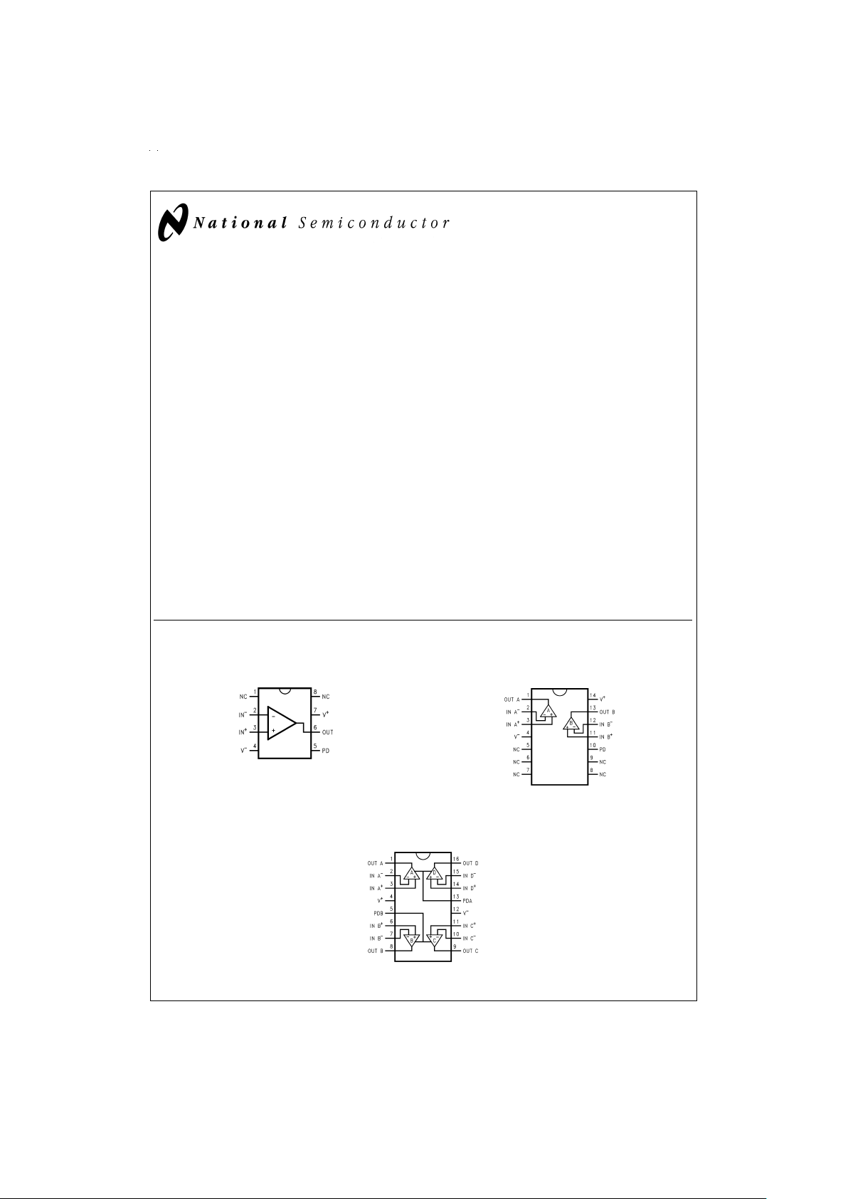
Connection Diagrams
8-Pin DIP/SO
DS012042-1
Top View
14-Pin DIP/SO
DS012042-2
Top View
16-Pin DIP/SO
DS012042-3
Top View
May 1995
LMC6681 Single/LMC6682 Dual/LMC6684 Quad Low Voltage, Rail-To-Rail Input and Output CMOS
Amplifier with Powerdown
© 1999 National Semiconductor Corporation DS012042 www.national.com
Page 2
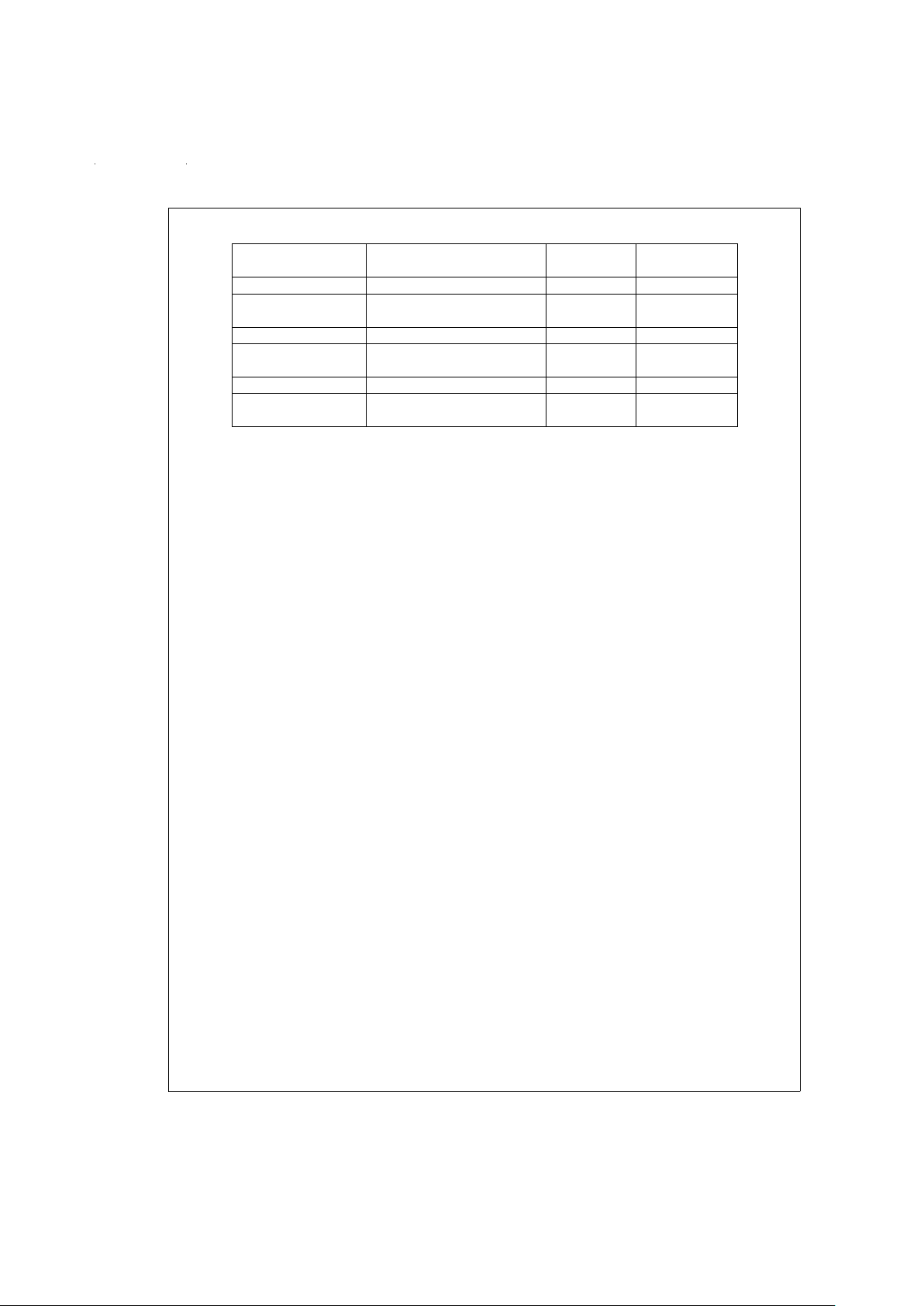
Ordering Information
Package Temperature Range NSC Transport
Industrial, −40˚C to +85˚C Drawing Media
8-Pin Molded DIP LMC6681AIN, LMC6681BIN N08E Rails
8-Pin Small Outline LMC6681AIM, LMC6681BIM M08A Rails
LMC6681AIMX, LMC6681B1MX M08A Tape and Reel
14-Pin Molded DIP LMC6682AIN, LMC6682BIN N14A Rails
14-Pin Small Outline LMC6682AIM, LMC6682BIM M14A Rails
LMC6682AIMX, LMC6682BIMX M14A Tape and Reel
16-Pin Molded DIP LMC6684AIN, LMC6684BIN N16A Rails
16-Pin Small Outline LMC6684AIM, LMC6684BIM M16A Rails
LMC6684AIMX, LMC6684BIMX M16A Tape and Reel
www.national.com 2
Page 3
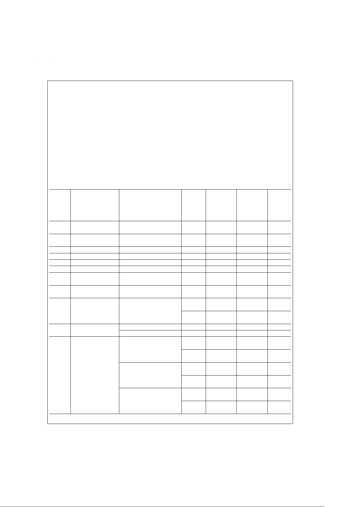
Absolute Maximum Ratings (Note 1)
If Military/Aerospace specified devices are required,
please contact the National Semiconductor Sales Office/
Distributors for availability and specifications.
ESD Tolerance (Note 2) 2 kV
Differential Input Voltage
±
Supply Voltage
Voltage at Input/Output Pin (V
+
) +0.3V, (V−) −0.3V
Supply Voltage (V
+
− V−) 12V
Current at Input Pin (Note 11)
±
5mA
Current at Output Pin (Note 3)
±
30 mA
Current at Power Supply Pin 35 mA
Lead Temp. (soldering, 10 sec.) 260˚C
Storage Temperature Range −65˚C to +150˚C
Junction Temperature (Note 4) 150˚C
Operating Ratings (Note 1)
Supply Voltage 1.8V ≤ V
S
≤ 10V
Junction Temperature Range
LMC6681AI, LMC6681BI −40˚C ≤ T
J
≤ +85˚C
LMC6682AI, LMC6682BI −40˚C ≤ T
J
≤ +85˚C
LMC6684AI, LMC6684BI −40˚C ≤ T
J
≤ +85˚C
Thermal Resistance (θ
JA
)
N Package, 8-pin Molded DIP 108˚C/W
M Package, 8-pin Surface Mount 172˚C/W
N Package, 14-pin Molded DIP 88˚C/W
M Package, 14-pin Surface Mount 126˚C/W
N Package, 16-pin Molded DIP 83˚C/W
M Package, 16-pin Surface Mount 114˚C/W
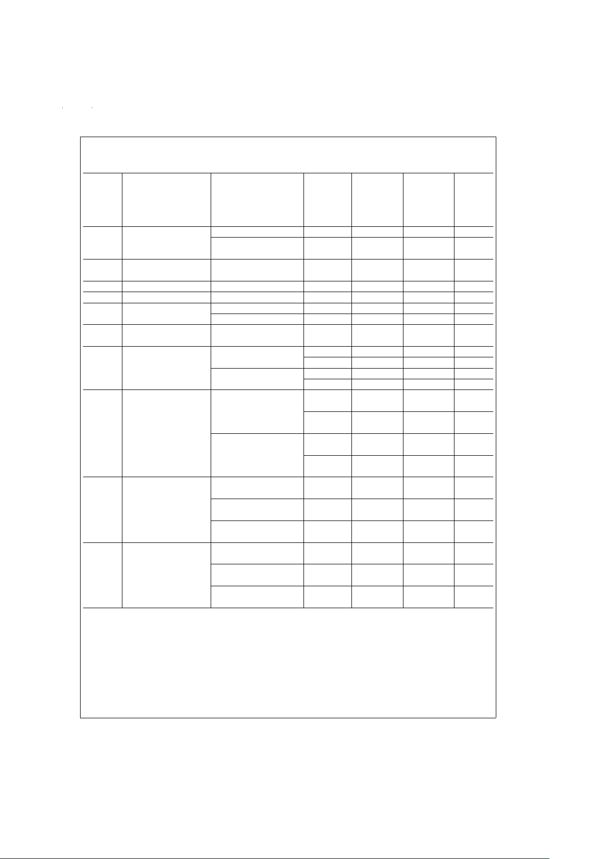
3V DC Electrical Characteristics
Unless otherwise specified, all limits guaranteed for T
J
=
25˚C, V
+
=
3.0V, V−=0V, V
CM
=
V
O
=
V
+
/2, V
PD
=
0.6V and R
L
>
1MΩ.Boldface limits apply at the temperature extremes (Note 16).
Symbol Parameter Conditions
Typ
(Note 5)
LMC6681AI LMC6681BI
Units
LMC6682AI LMC6682BI
LMC6684AI LMC6684BI
Limit Limit
(Note 6) (Note 6)
V
OS
Input Offset Voltage 0.5 1 3 mV
2.5 4.5 max
TCV
OS
Input Offset Voltage 1.5 µV/˚C
Average Drift
I
B
Input Current (Note 12) 0.08 20 20 pA max
I
OS
Input Offset Current (Note 12) 0.04 10 10 pA max
R
IN
Input Resistance
>
1 Tera Ω
C
IN
Input Capacitance 3 pF
CMRR Common Mode (Note 13) 82 70 65 dB
Rejection Ratio 65 62 min
PSRR Power Supply
±
1.5V ≤ VS≤±2.5V 82 70 65 dB
Rejection Ratio V
O
=
V
+
/2=V
CM
65 62 min
V
CM
Input Common Mode CMRR>50 dB 3.23 3.18 3.18 V
Voltage Range 3.00 3.00 min
−0.3 −0.18 −0.18 V
0.00 0.00 max
A
V
Large Signal
Voltage Gain
R
L
=
600Ω (Notes 7, 12) 70 10 10 V/mV
R
L
=
10 kΩ (Notes 7, 12) 1000 12 12 V/mV
V
O
Output Swing R
L
=
600Ω to V
+
/2 2.87 2.70 2.70 V
2.58 2.58 min
0.15 0.3 0.3 V
0.42 0.42 max
R
L
=
2kΩto V
+
/2 2.95 2.85 2.85 V
2.79 2.79 min
0.05 0.15 0.15 V
0.21 0.21 max
R
L
=
10 kΩ to V
+
/2 2.99 2.94 2.94 V
2.91 2.91 min
0.01 0.04 0.04 V
0.05 0.05 max
www.national.com3
Page 4
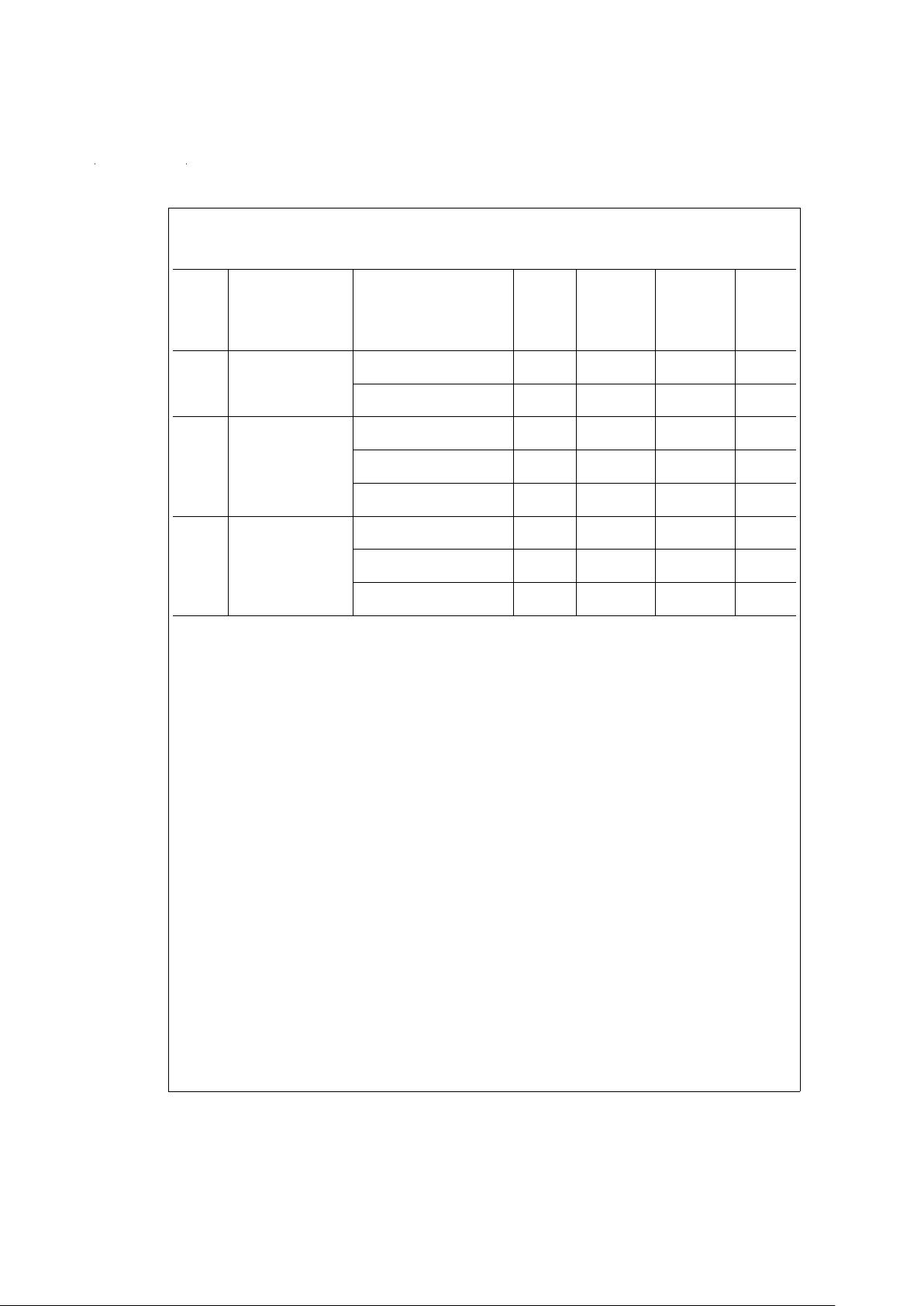
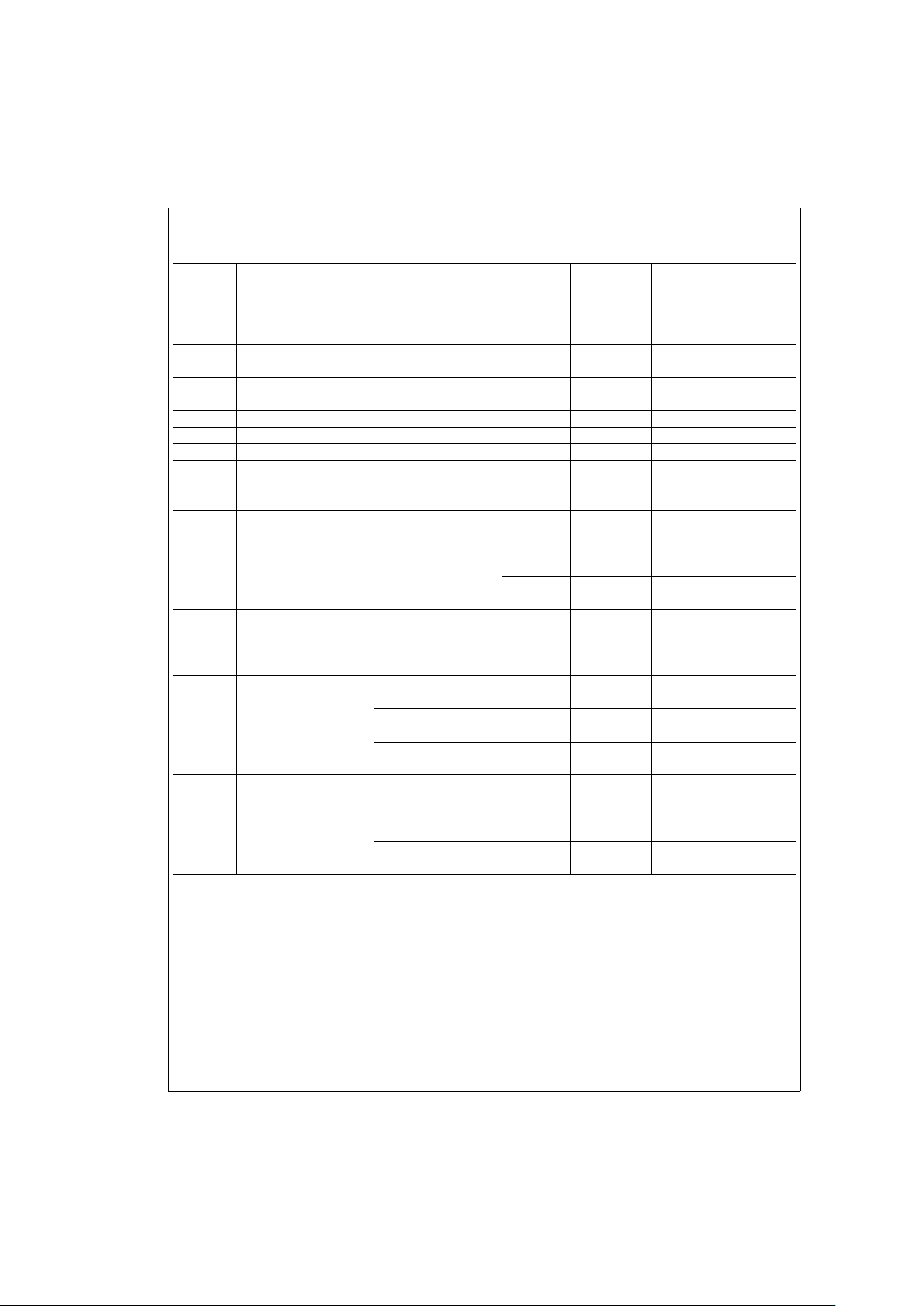
3V DC Electrical Characteristics (Continued)
Unless otherwise specified, all limits guaranteed for T
J
=
25˚C, V
+
=
3.0V, V−=0V, V
CM
=
V
O
=
V
+
/2, V
PD
=
0.6V and R
L
>
1MΩ.Boldface limits apply at the temperature extremes (Note 16).
Symbol Parameter Conditions
Typ
(Note 5)
LMC6681AI LMC6681BI
Units
LMC6682AI LMC6682BI
LMC6684AI LMC6684BI
Limit Limit
(Note 6) (Note 6)
I
SC
Output Short Sourcing, V
O
=
0V 20 9.0 9.0 mA
Circuit Current 6.7 6.7 min
Sinking, V
O
=
3V 12 6.0 6.0 mA
4.5 4.5 min
I
SON
Supply Current Single, LMC6681 0.7 1.13 1.13 mA
when Powered ON V
CM
=
1.5V 1.36 1.36 max
Dual, LMC6682 1.4 2.26 2.26 mA
V
CM
=
1.5V 2.75 2.75 max
Quad, LMC6684 2.8 4.52 4.52 mA
V
CM
=
1.5V 5.42 5.42 max
I
S OFF
Supply Current Single, LMC6681 0.5 1.5 1.5 µA
when Powered OFF V
PD
=
2.3V 2.1 2.1 max
Dual, LMC6682 0.5 1.5 1.5 µA
V
PD
=
2.3V 2.1 2.1 max
Quad, LMC6684 1.0 3.0. 3.0 µA
V
PD
=
2.3V 4.2 4.2 max
www.national.com 4
Page 5
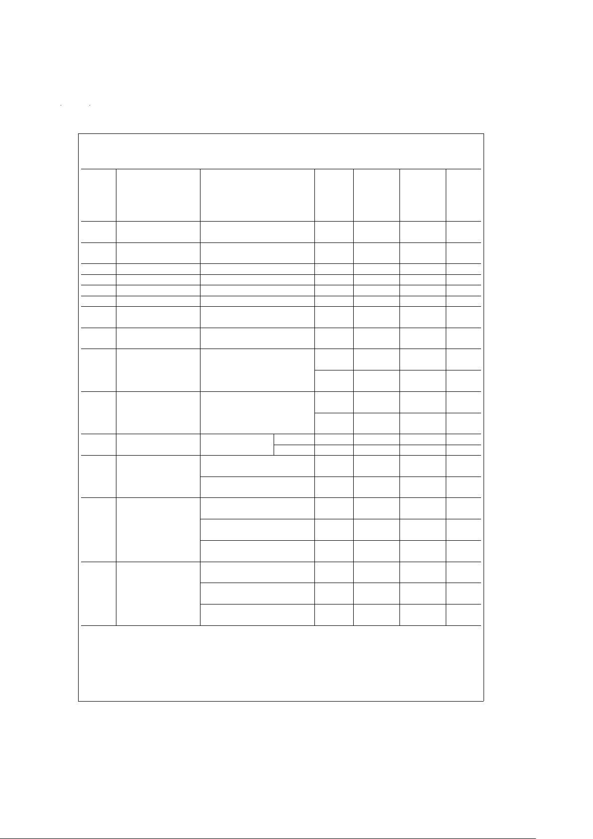
1.8V and 2.2V DC Electrical Characteristics
Unless otherwise specified, all limits guaranteed for T
J
=
25˚C, V+=1.8V and 2.2V, V−=0V, V
CM
=
V
O
=
V
+
/2, V
PD
=
0.4V
(
@
2.2V), V
PD
=
0.3V (
@
1.8V) and R
L
>
1MΩ.Boldface limits apply at the temperature extremes (Note 16).
LMC6681AI LMC6681BI
Typ LMC6682AI LMC6682BI
Symbol Parameter Conditions (Note 5) LMC6684AI LMC6684BI Units
Limit Limit
(Note 6) (Note 6)
V
OS
Input Offset Voltage V
+
=
1.8V, V
CM
=
1.5V 0.5 3 10 mV max
V
+
=
2.2V, V
CM
=
1.5V 0.5 2 6 mV
3.8 7.8 max
TCV
OS
Input Offset Voltage V
+
=
2.2V 1.5 µV/˚C
Average Drift
I
B
Input Current V
+
=
2.2V (Note 12) 0.08 20 20 pA max
I
OS
Input Offset Current V
+
=
2.2V (Note 12) 0.04 10 10 pA max
CMRR Common Mode V
+
=
2.2V (Note 13) 82 60 60 dB min
Rejection Ratio V
+
=
1.8V (Note 13) 82 50 50 dB min
PSRR Power Supply
±
1.1V ≤ VS≤±5V, 82 70 65 dB
Rejection Ratio V
O
=
V
+
/2=V
CM
65 62 min
V
CM
Input Common Mode V
+
=
2.2V
CMRR
>
40 dB
2.38 2.2 2.2 V min
Voltage Range −0.15 0.0 0.0 V max
V
+
=
1.8V
CMRR
>
40 dB
1.98 1.8 1.8 V min
−0.10 0.0 0.0 V max
V
O
Output Swing V
+
=
2.2V 2.15 2.0 2.0 V
R
L
=
2kΩto V
+
/2 1.88 1.88 min
0.05 0.2 0.2 V
0.32 0.32 max
V
+
=
1.8V 1.75 1.6 1.6 V
R
L
=
2kΩto V
+
/2 1.44 1.44 min
0.05 0.2 0.2 V
0.32 0.32 max
I
SON
Supply Current Single, LMC6681 0.7 1.1 1.1 mA
when Powered ON V
CM
=
1.5V 1.32 1.32 max
Dual, LMC6682 1.4 2.2 2.2 mA
V
CM
=
1.5V 2.7 2.7 max
Quad, LMC6684 2.8 4.4 4.4 mA
V
CM
=
1.5V 5.3 5.3 max
I
S OFF
Supply Current Single, LMC6681 0.5 1.5 1.5 µA
when Powered OFF V
PD
=
1.5V 2.7 2.7 max
Dual, LMC6682 0.5 1.5 1.5 µA
V
PD
=
1.5V 2.7 2.7 max
Quad, LMC6684 1.0 3.0 3.0 µA
V
PD
=
1.5V 5.4 5.4 max
www.national.com5
Page 6
5V DC Electrical Characteristics
Unless otherwise specified, all limits guaranteed for T
J
=
25˚C, V
+
=
5.0V, V−=0V, V
CM
=
V
O
=
V
+
/2, V
PD
=
0.9V and R
L
>
1MΩ.Boldface limits apply at the temperature extremes (Note 16).
Symbol Parameter Conditions
Typ
(Note 5)
LMC6681AI LMC6681BI
Units
LMC6682AI LMC6682BI
LMC6684AI LMC6684BI
Limit Limit
(Note 6) (Note 6)
V
OS
Input Offset Voltage V
CM
=
1.5V 0.5 1 3 mV
2.5 4.5 max
TCV
OS
Input Offset Voltage 1.5 µV/˚C
Average Drift
I
B
Input Current (Note 12) 0.08 20 20 pA max
I
OS
Input Offset Current (Note 12) 0.04 10 10 pA max
R
IN
Input Resistance
>
1 Tera Ω
C
IN
Input Capacitance 3 pF
CMRR Common Mode (Note 13) 82 70 65 dB
Rejection Ratio 65 62 min
PSRR Power Supply Rejection
±
1.5V ≤ VS≤±2.5V 82 70 65 dB
Ratio V
O
=
V
+
/2=V
CM
65 62 min
V
CM
Input Common Mode CMRR>50 dB 5.3 5.18 5.18 V
Voltage Range 5.00 5.00 min
−0.3 −0.18 −0.18 V
0.00 0.00 max
V
O
Output Swing R
L
=
2kΩto V
+
/2 4.9 4.85 4.85 V
4.58 4.58 min
0.05 0.2 0.2 V
0.28 0.28 max
I
SON
Supply Current Single, LMC6681 0.8 1.24 1.24 mA
when Powered ON V
CM
=
1.5V 1.49 1.49 max
Dual, LMC6682 1.5 2.48 2.48 mA
V
CM
=
1.5V 3.00 3.00 max
Quad, LMC6684 3.0 4.96 4.96 mA
V
CM
=
1.5V 6.00 6.00 max
I
S OFF
Supply Current Single, LMC6681 0.5 1.5 1.5 µA
when Powered OFF V
PD
=
4.3V 2.1 2.1 max
Dual, LMC6682 0.5 1.5 1.5 µA
V
PD
=
4.3V 2.1 2.1 max
Quad, LMC6684 1.0 3.0 3.0 µA
V
PD
=
4.3V 4.2 4.2 max
www.national.com 6
Page 7
10V DC Electrical Characteristics
Unless otherwise specified, all limits guaranteed for T
J
=
25˚C, V
+
=
10.0V, V−=0V, V
CM
=
V
O
=
V
+
/2, V
PD
=
1.2V and R
L
>
1MΩ.Boldface limits apply at the temperature extremes (Note 16).
Symbol Parameter Conditions
Typ
(Note 5)
LMC6681AI LMC6681BI
Units
LMC6682AI LMC6682BI
LMC6684AI LMC6684BI
Limit Limit
(Note 6) (Note 6)
V
OS
Input Offset Voltage V
CM
=
1.5V 0.5 1.5 3.5 mV
3.0 5.0 max
TCV
OS
Input Offset Voltage 1.5 µV/˚C
Average Drift
I
B
Input Current (Note 12) 0.08 20 20 pA max
I
OS
Input Offset Current (Note 12) 0.04 10 10 pA max
R
IN
Input Resistance
>
1 Tera Ω
C
IN
Input Capacitance 3 pF
CMRR Common Mode (Note 13) 82 65 65 dB
Rejection Ratio 62 62 min
PSRR Positive Power Supply
±
1.1V ≤ VS≤±5V 82 70 65 dB
Rejection Ratio V
O
=
V
+
/2 65 62 min
V
CM
Input Common Mode CMRR>50 dB 10.30 10.18 10.18 V
Voltage Range 10.00 10.00 min
−0.30 −0.18 −0.18 V
0.00 0.00 max
V
O
Output Swing R
L
=
2kΩto V
+
/2 9.93 9.7 9.7 V
9.58 9.58 min
0.08 0.3 0.3 V
0.42 0.42 max
A
V
Large Signal R
L
=
2kΩto V
+
/2 Sourcing 89 25 25 V/mV
Voltage Gain (Note 12) Sinking 224 25 25 V/mV
I
SC
Output Short Circuit Sourcing, V
O
=
0V 65 30 30 mA
Current (Note 14) 22 22 min
Sinking, V
O
=
10V 70 30 30 mA
(Note 14) 22 22 min
I
SON
Supply Current Single, LMC6681 0.9 1.50 1.50 mA
when Powered ON V
CM
=
1.5V 1.8 1.8 max
Dual, LMC6682 1.6 3.00 3.00 mA
V
CM
=
1.5V 3.6 3.6 max
Quad, LMC6684 3.2 6.00 6.00 mA
V
CM
=
1.5V 7.2 7.2 max
I
S OFF
Supply Current Single, LMC6681 0.5 5 5 µA
when Powered OFF V
PD
=
9.3V 77max
Dual, LMC6682 0.5 5 5 µA
V
PD
=
9.3V 77max
Quad, LMC6684 1.0 10 10 µA
V
PD
=
9.3V 14 14 max
www.national.com7
Page 8
Powerdown DC Threshold Characteristics
Boldface limits apply at the temperature extremes (Note 16).
Symbol Parameter Conditions
LMC6681AI, LMC6681BI
Units
LMC6682AI, LMC6682BI
LMC6684AI, LMC6684BI
Min Typ Max
V
PD, IL
Powerdown Voltage Input Low (Device V
+
=
2.2V 0.4 V
Powered ON; Amplifier meets all V
−
=
0V 0.25
specs in the datasheet tables) V
+
=
3V 0.6 V
V
−
=
0V 0.45
V
+
=
5V 0.9 V
V
−
=
0V 0.75
V
+
=
10V 1.2 V
V
−
=
0V 1.05
V
PD, IH
Powerdown Voltage Input High (Device V
+
=
2.2V 1.5 V
Powered OFF; Refer to DC Electrical V
−
=
0V 1.65
Characteristics for I
S OFF
specs) V
+
=
3V 2.3 V
V
−
=
0V 2.45
V
+
=
5V 4.3 V
V
−
=
0V 4.45
V
+
=
10V 9.3 V
V
−
=
0V 9.45
www.national.com 8
Page 9

AC Electrical Characteristics
Unless otherwise specified, all limits guaranteed for T
J
=
25˚C, V
+
=
3V, V−=0V, V
CM
=
V
O
=
V
+
/2, V
PD
=
0.6V and R
L
>
1
MΩ. Boldface limits apply at the temperature extremes (Note 16).
Symbol Parameter Conditions
Typ
(Note 5)
LMC6681AI LMC6681BI
Units
LMC6682AI LMC6682BI
LMC6684AI LMC6684BI
Limit Limit
(Note 6) (Note 6)
t
ON
Time Delay for (Note 15) 50 200 200 µs
Device to Power ON
t
OFF
Time Delay for (Note 15) 0.5 2 2 µs
Device to Power OFF
SR Slew Rate (Note 8) 1.2 0.7 0.7
V/µs
min
0.55 0.55
V
+
=
10V, (Note 10) 1.2 0.7 0.7
0.55 0.55
GBW Gain-Bandwidth Product 1.2 MHz
φ
m
Phase Margin 50 Deg
G
m
Gain Margin 12 dB
Amp-to-Amp Isolation V
+
=
10V (Note 9) 130 dB
e
n
Input-Referred f=1 kHz
32
Voltage Noise V
CM
=
0.5V
i
n
Input-Referred f=1 kHz
0.5
Current Noise
T.H.D. Total Harmonic Distortion f=1 kHz, A
V
=
+1 0.01
%
R
L
=
10 kΩ,V
O
=
2V
PP
Note 1: Absolute Maximum Ratings indicate limits beyond which damage to the device may occur. Operating ratings indicate conditions for which the device is intended to be functional, but specific performance is not guaranteed. For guaranteed specifications and the test conditions, see the electrical characteristics.
Note 2: Human body model, 1.5 kΩ in series with 100 pF.
Note 3: Applies to both single-supply and split-supply operation. Continous short circuit operationatelevatedambienttemperature can result in exceeding the maxi-
mum allowed junction temperature of 150˚C. Output current in excess of
±
30 mA over long term may adversely affect reliability.
Note 4: The maximum power dissipation is a function of T
J (max)
, θJA, and TA. The maximum allowable power dissipation at any ambient temperature is P
D
=
(T
J(max)
−TA)/θJA. All numbers apply for packages soldered directly into a PC board.
Note 5: Typical Values represent the most likely parametric norm.
Note 6: All limits are guaranteed by testing or statistical analysis.
Note 7: V
+
=
3V, V
CM
=
0.5V. For sourcing and sinking, 0.5V ≤ V
O
≤ 2.5V.
Note 8: V
+
=
3V. Connected as Voltage Follower with 2V step input, and the output is measured from 15%–85%. Number specified is the slower of the positive or
negative slew rates.
Note 9: Input referred, V
+
=
10V, and R
L
=
100 kΩ connected to 5V. Each amp excited in turn with 1 kHz to produce V
O
=
2V
PP
.
Note 10: V
+
=
10V.Connected as voltage follower with 8V step Input, and output is measured from 15%–85%. Number specified is the slower of the positive or nega-
tive slew rates.
Note 11: Limiting input pin current is only necessary for input voltages that exceed absolute maximum input voltage ratings.
Note 12: Guaranteed limits are dictated by tester limitations and not device performance. Actual performance is reflected in the typical value.
Note 13: CMRR
+
and CMRR−are tested, and the number indicated is the lower of the two values. For CMRR+,V+/2<V
CM
<
V+for 1.8V, 2.2V, 3V, 5V, and 10V.
For CMRR
−
,0<V
CM
<
V+/2 for 3V, 5V and 10V. For 1.8V and 2.2V, 0.25<V
CM
<
V+− 0.3.
Note 14: V
+
=
10V, V
CM
=
0.5V. For Sourcing tests, 1V ≤ V
O
≤ 5V. For Sinking tests, 5V ≤ VO≤ 9V.
Note 15: The propogation delays are measured using an input waveform of f=5 Hz, and magnitude of 2.4V. Refer to Section 6.3 and
Figures 14, 15
for a detailed
explanation.
Note 16: The V
PD
(threshold low and threshold high) limits are guaranteed at room temperature and at temperature extremes. Room temperature limits are production tested. Limits at temperature extremes are guaranteed via correlation using temperature regression analysis methods. Refer to Section 6.2 for an overview of
the threshold voltages.
www.national.com9
Page 10

Typical Performance Characteristics V
S
+=3V, Single Supply, T
A
=
25˚C unless otherwise specified
Supply Current per Amplifier
vs Supply Voltage
DS012042-40
Sourcing Current
vs Output Voltage
DS012042-41
Sinking Current
vs Output Voltage
DS012042-42
Input Voltage Noise
vs Common-Mode Voltage
DS012042-43
∆VOSvs V
CM
DS012042-44
∆VOSvs V
CM
DS012042-45
Frequency Response
vs Temperature
DS012042-46
Frequency Response
vs R
L
DS012042-47
Input Voltage Noise
vs Frequency
DS012042-48
www.national.com 10
Page 11

Typical Performance Characteristics V
S
+=3V, Single Supply, T
A
=
25˚C unless otherwise
specified (Continued)
CMRR
vs Frequency
DS012042-49
Positive PSRR
vs Frequency
DS012042-50
Negative PSRR
vs Frequency
DS012042-51
Crosstalk Rejection
vs Frequency
DS012042-52
Slew Rate vs
Supply Voltage
DS012042-53
Non-Inverting Large
Signal Pulse Response
DS012042-54
Inverting Large
Signal Pulse Response
DS012042-55
Non-Inverting Small
Signal Pulse Response
DS012042-56
Inverting Small
Signal Pulse Response
DS012042-57
www.national.com11
Page 12

Typical Performance Characteristics V
S
+=3V, Single Supply, T
A
=
25˚C unless otherwise
specified (Continued)
Stability vs
Capacitive Load
DS012042-58
Stability vs
Capacitive Load
DS012042-59
Stability vs
Capacitive Load
DS012042-60
tONDelay till Active-On
after t
PD OFF
in
Powerdown Mode, V
S
=
3V
DS012042-39
www.national.com 12
Page 13

Application Information
1.0 Input Common-Mode Voltage
Range
The LMC6681/2/4 has a rail-to-rail input common-mode voltage range.
Figure 1
shows an input voltage exceeding both
supplies with no resulting phase inversion on the output.
The absolute maximum input voltage at V
+
=
3V is 300 mV
beyond either supply rail at room temperature. Voltages
greatly exceeding this absolute maximum rating, as in
Figure
2
, can cause excessive current to flow in or out of the input
pins, possibly affecting reliability. The input current can be
externally limited to
±
5 mA, with an input resistor, as shown
in
Figure 3
.
2.0 Rail-to-Rail Output
The approximated output resistance of the LMC6681/2/4 is
50Ω sourcing, and 50Ω sinking at V
S
=
3V. The maximum
output swing can be estimated as a function of load using the
calculated output resistance.
3.0 Low Voltage Operation
The LMC6682 operates at supply voltages of 2.2V and 1.8V.
These voltages represent the End of Discharge voltages of
several popular batteries. The amplifier can operate from 1
Lead-Acid or Lithium Ion battery, or 2NiMH, NiCd, or
Carbon-Zinc batteries. Nominal and End of Discharge of
Voltage of several batteries are listed below.
Battery Type Nominal Voltage End of Discharge
Voltage
NiMH 1.2V 1V
NiCd 1.2V 1V
Lead-Acid 2V 1.8V
Silver Oxide 1.6V 1.3V
Carbon-Zinc 1.5V 1.1V
Lithium 2.6V–3.6V 1.7V–2.4V
At V
S
=
2.2V, the LMC6681/2/4 has a rail-to-rail input
common-mode voltage range.
Figure 4
shows an input volt-
age extending to both supplies and the resulting output.
The amplifier is operational at V
S
=
1.8V,with guaranteed input common-mode voltage range, output swing, and CMRR
specs.
Figure 5
shows the response of the LMC6681/2/4 at
V
S
=
1.8V.
DS012042-5
FIGURE 1. An Input Signal Exceeds the LMC6681/2/4
Power Supply Voltages with No Output Phase
Inversion
DS012042-6
FIGURE 2. A±7.5V Input Signal Greatly
Exceeds the 3V Supply in
Figure 3
,
Causing No Phase Inversion Due to R
I
DS012042-7
FIGURE 3. Input Current Protection for
Voltages Exceeding the Supply Voltage
DS012042-8
FIGURE 4. The Input Common-Mode Voltage
Range Extends to Both Supplies at V
S
=
2.2V
DS012042-9
FIGURE 5. Response of the LMC6681/2/4
at V
S
=
1.8V
www.national.com13
Page 14

3.0 Low Voltage Operation (Continued)
Figure 6
shows an input voltage exceeding both supplies
with no resulting phase inversion on the output.
4.0 Capacitive Load Tolerance
The LMC6681/2/4 can typically drive a 100 pF load with V
S
=
10V at unity gain without oscillating. The unity gain follower is the most sensitive configuration to capacitive load.
Direct capacitive loading reduces the phase margin of
op-amps. The combination of the op-amp’s output impedance and the capacitive load induces phase lag. This results
in either an underdamped pulse response or oscillation.
Capacitive load compensation can be accomplished using
resistive isolation as shown in
Figure 7
. If there is a resistive
component of the load in parallel to the capacitive component, the isolation resistor and the resistive load create a
voltage divider at the output. This introduces a DC error at
the output.
Figure 8
displays the pulse response of the LMC6681 circuit
in
Figure 7
.
Another circuit, shown in
Figure 9
, is also used to indirectly
drive capacitive loads. This circuit is an improvement to the
circuit shown
Figure 7
because it provides DC accuracy as
well as AC stability. R1 and C1 serve to counteract the loss
of phase margin by feeding the high frequency component of
the output signal back to the amplifiers inverting input,
thereby preserving phase margin in the overall feedback
loop. The values of R1 and C1 should be experimentally determined by the system designer for the desired pulse response. Increased capacitive drive is possible by increasing
the value of the capacitor in the feedback loop.
DS012042-10
FIGURE 6. An Input Voltage Signal Exceeds
LMC6681/2/4 Power Supply Voltages of
V
S
=
1.8V with No Output Phase Inversion
DS012042-11
FIGURE 7. Resistive Isolation
of a 350 pF Capacitive Load
DS012042-12
FIGURE 8. Pulse Response of the
LMC6681 Circuit in
Figure 7
DS012042-13
FIGURE 9. The LMC6682 Compensated
to Ensure DC Accuracy and AC Stability
www.national.com 14
Page 15

4.0 Capacitive Load Tolerance (Continued)
The pulse response of the circuit shown in
Figure 9
is shown in
Figure 10
.
Application Hints
5.0 Printed-Circuit-Board Layout for High-Impedance Work
It is generally recognized that any circuit which must operate
with less than 1000 pA of leakage current requires special
layout of the PC board. When one wishes to take advantage
of the ultra-low input current of the LMC6681/2/4, typically
less than 80 fA, it is essential to have an excellent layout.
Fortunately, the techniques of obtaining low leakages are
quite simple. First, the user must not ignore the surface leakage of the PC board, even though it may sometimes appear
acceptably low,because under conditions of high humidity or
dust or contamination, the surface leakage will be appreciable.
To minimize the effect of any surface leakage, lay out a ring
of foil completely surrounding the LMC6681/2/4’s inputs and
the terminals of capacitors, diodes, conductors, resistors, relay terminals, etc. connected to the op-amp’s inputs, as in
Figure 11
. Tohave a significant effect, guard rings should be
placed in both the top and bottom of the PC board. This PC
foil must then be connected to a voltage which is at the same
voltage as the amplifier inputs, since no leakage current can
flow between two points at the same potential. For example,
a PC board trace-to-pad resistance of 10
12
Ω, which is normally considered a very large resistance, could leak 5 pA if
the trace were a 5V bus adjacent to the pad of the input.This
would cause a 60 times degradation from the LMC6681/2/
4’s actual performance. However, if a guard ring is held
within 5 mV of the inputs, then even a resistance of 10
11
Ω
would cause only 0.05 pA of leakage current. See
Figure 12
for typical connections of guard rings for standard op-amp
configurations.
DS012042-14
FIGURE 10. Pulse Response of the
LMC6682 Circuit Shown in
Figure 9
DS012042-18
FIGURE 11. Example of Guard Ring in PC Board
Layout
www.national.com15
Page 16

5.0 Printed-Circuit-Board Layout
for High-Impedance Work
(Continued)
The designer should be aware that when it is inappropriate
to lay out a PC board for the sake of just a few circuits, there
is another technique which is even better than a guard ring
on a PC board: Don’t insert the amplifier’s input pin into the
board at all, but bend it up in the air and use only air as an insulator. Air is an excellent insulator. In this case you may
have to forego some of the advantages of PC board construction, but the advantages are sometimes well worth the
effort of using point-to-point up-in-the-air wiring. See
Figure
13
.
6.0 Powerdown
6.1 PINOUT FOR THE LMC6681/LMC6682/LMC6684
For the LMC6681/2/4, the input, output, and power pins are
the same as those used in the standard configuration. One
of the other pins, pin 5 in the case of the LMC6681, is used
to enable the powerdown mode. The connection diagrams
for the LMC6681/2/4 are on the front page of the datasheet.
The LMC6684 has 2 powerdown options. Each of the powerdown pins disables two amplifiers. If both the powerdown
pins are pulled high, all four amplifiers will be disabled. Referring to the connection diagrams on the front page of the
datasheet, Pin 5 disables amplifiers B and C and Pin 13 disables amplifiers A and D.
6.2 EXPLANATION OF DATASHEET PARAMETERS
The LMC6681/2/4 is ON (meets all the datasheet specs)
when the voltage applied to the powerdown pin, V
PD
is a
logic low. The device is OFF when V
PD
is a logic high. These
logic levels are indicated in the test conditions in the
datasheet tables. Summarizing these numbers:
Supply Logic High [V] Logic Low [V]
Voltage at room over temp at room over temp
2.2V V
PD
≥ 1.5 VPD≥ 1.65 VPD≤ 0.4 VPD≤ 0.25
3V V
PD
≥ 2.3 VPD≥ 2.45 VPD≤ 0.6 VPD≤ 0.45
5V V
PD
≥ 4.3 VPD≥ 4.45 VPD≤ 0.9 VPD≤ 0.75
10V V
PD
≥ 9.3 VPD≥ 9.45 VPD≤ 1.2 VPD≤ 1.05
In applications where the powerdown pin is not connected
externally, it is pulled to a logic low internally through a current source. The t
ON
and t
OFF
specs will essentially be the
same for a V
PD
in the specified range. This means that the
LMC6681/2/4 will typically be fully operational 50 µs after a
logic low has been applied to the powerdown pin. Please
note that the frequency of V
PD
in the test circuit below is
5 Hz.
DS012042-19
Inverting Amplifier
DS012042-20
Non-Inverting Amplifier
DS012042-21
Follower
FIGURE 12. Typical Connections of Guard Rings
DS012042-22
(Input pins are lifted out of PC board and soldered directly to components.
All other pins are connected to PC board.)
FIGURE 13. Air Wiring
www.national.com 16
Page 17

6.0 Powerdown (Continued)
6.3 TEST CIRCUIT TO MEASURE t
ON
AND t
OFF
The circuit used to measure the tON, and t
OFF
during the
powerdown operation is a voltage follower with a load of
2kΩas shown in
Figure 14
.
When the input to the powerdown pin is low, the LMC6681/
2/4 is on. Since the amplifier is connected in the voltage follower configuation, the output of the circuit is −1V.When the
powerdown pin is pulled high, the amplifier shuts down, and
draws less than 1 µA/Amplifier. In this powerdown mode, the
output pin has high impedance, and the output of the circuit
is pulled to 0V. t
ON
is specified as the time between the 50
%
points of the trailing edges of the input waveform at the powerdown pin, and the waveform at the output pin. Similarly,
the t
OFF
is specified as the time between the 50%points of
the leading edges of the input waveform at the powerdown
pin, and the waveform at the output pin.
6.4 t
ON
and t
OFF
The tON(time delay for device to power on) the t
OFF
(time delay for device to power off) specs are guaranteed at a supply
voltage of 3V.The t
ON
and t
OFF
spec are independent of the
V
PD
applied in the specified range. Refer to the Powerdown
DC Threshold Characteristics table for the values for a logic
low and a logic high.
The guaranteed spec for t
ON
is 200 µs. This does not mean
that the signal to the V
PD
pin can be as high as 5 kHz (1/200
µs). Note that the V
PD
frequency for the tONand t
OFF
measurements is 5 Hz. The LMC6681/2/4 is ideal for DC type applications where the powerdown pin is controlled by low frequency signals.
When the LMC6681/2/4 is powered off, internal bias currents
are shutoff. There is a inherent latency in the circuit, and the
device has to power off for a certain period of time for the t
ON
spec to apply.Refer to the figure below. t
PD OFF
refers to the
time interval for which the device is in the powerdown mode.
Consider the case when the device has been powered off for
5 ms, and then the powerdown pin is pulled to a logic low.
From
Figure 16
, at room temperature, the device powers on
after 500 µs.
DS012042-16
FIGURE 14. Test Circuit for tONand t
OFF
Measurements
DS012042-17
(a) t
OFF
Measurement
DS012042-29
(b) tONMeasurement
FIGURE 15.
DS012042-39
FIGURE 16. tONDelay Till Active-On after
t
PDOFF
in Powerdown Mode, V
S
=
3V
www.national.com17
Page 18

7.0 Compensating for Input
Capacitance
It is quite common to use large values of feedback resistance with amplifiers that have ultra-low input current, like
the LMC6681/2/4. Large feedback resistors can react with
small values of input capacitance due to transducers, photodiodes, and circuits board parasitics to reduce phase
margins.
The effect of input capacitance can be compensated for by
adding a feedback capacitor. The feedback capacitor (as in
Figure 17
), CF, is first estimated by:
or
R1C
IN
≤
R2C
F
which typically provides significant overcompensation.
Printed circuit board stray capacitance may be larger or
smaller than that of a breadboard, so the actual optimum
value for C
F
may be different. The values of CFshould be
checked on the actual circuit. (Refer to the LMC660 quad
CMOS amplifier data sheet for a more detailed discussion.)
8.0 Spice Macromodel
A Spice Macromodel is available for the LMC6681/2/4. The
model includes a simulation of:
•
Input common-mode voltage range
•
Frequency and transient response
•
GBW dependence on loading conditions
•
Quiescent and dynamic supply current
•
Output swing dependence on loading conditions
and many more characteristics as listed on the macromodel
disk.
Contact the National Semiconductor Customer Response
Center at 1-800-272-9959 to obtain an operational amplifier
spice macromodel library disk.
Applications
Transducer Interface Circuits
A. PIEZOELECTRIC TRANSDUCERS
The LMC6681 can be used for processing of transducer signals as shown in the circuit below. The two 11 MΩ resistors
provide a path for the DC currents to ground. Since the resistors are bootstrapped to the output, the AC input resistance
of the LMC6681 is much higher.
An input current of 80 fA and a CMRR of 82 dB causes an insignificant error offset voltage at the output. The rail-to-rail
performance of the amplifier also provides the maximum dynamic range for the transducer signals.
B. PHOTODIODE AMPLIFIERS
Photocells can be used in light measuring instruments. An
error offset voltage is produced at the output due to the input
current and the offset voltage of the amplifier. The LMC6682,
which can be operated off a single battery is an excellent
choice for this application with its 80 fA input current and 0.5
mV offset voltage.
DS012042-15
FIGURE 17. Canceling the Effect of Input Capacitance
DS012042-24
FIGURE 18. Transducer Interface Application
DS012042-36
FIGURE 19. LMC6681 Used for Signal Processing
DS012042-26
FIGURE 20. Photodiode Amplifier
www.national.com 18
Page 19

Low Voltage Peak Detector
The accuracy of the peak detector is dependent on the leakage currents of the diodes and the capacitors, and the
non-idealities of the amplifier. The parameters of the amplifier which can limit the performance of this circuit are (a) Finite slew rate, (b) Input current, and (c) Maximum output current of the amplifier.
The input current of the amplifier causes a slow discharge of
the capacitor. This phenomenon is called “drooping”. The
LMC6682 has a typical input current of 80 fA. This would
cause the capacitor to droop at a rate of dV/dt=I
B
/C
=
80 fA/100 pF=0.8 mV/s. Accuracy in the amplitude measurement is also maintained by an offset voltage of 0.5 mV,
and an open-loop gain of 120 dB.
Oscillators
For single supply 5V operation, the output of the circuit will
swing from 0V to 5V. The voltage divider set up R
2,R3
and
R
4
will cause the non-inverting input of the LMC6681/2/4 to
move from 1.67V (
1
⁄3of 5V) to 3.33V (2⁄3of 5V). This voltage
behaves as the threshold voltage.
R
1
and C1determine the time constant for the circuit. The
frequency of oscillation, f
OSC
is
where ∆t is the time the amplifier input takes to move from
1.67V to 3.33V. The calculations are shown below.
where τ=RC=0.68 seconds
→
t
1
=
0.27 seconds.
and
→
t
2
=
0.74 seconds
Then,
LMC6681/2/4 as a Comparator
Figure 23
shows the application of the LMC6681/2/4 as a
comparator. The hysteresis is determined by the ratio of the
two resistors. Since the supply current of the LMC6681/2/4 is
less than 1 mA, it can be used as a low power comparator,in
applications where the quiescent current is an important parameter.At V
S
=
3V,typical propagation delays would be on
the order of t
PHL
=
6 µs, and t
PLH
=
5 µs.
Filters
The filter shown in
Figure 24
is used to process “voice-band”
signals. The bandpass filter has a gain of 40 dB. The two
corner frequencies, f
1
and f2are calculated as
DS012042-23
FIGURE 21. Low Voltage Peak Detector
DS012042-30
FIGURE 22. 1 Hz Square — Wave Oscillator
DS012042-31
FIGURE 23. Comparator with Hysteresis
DS012042-32
FIGURE 24. Wide-Band Band-Pass Filter
www.national.com19
Page 20

Filters (Continued)
The LMC6681/2/4, with its rail-to-rail input common-mode
voltage range and high gain (120 dB typical, R
L
=
10 kΩ)is
extremely well suited for such filter applications. The
rail-to-rail input range allows for large input signals to be processed without distortion. The high gain means that the circuit can provide filtering and gain in one stage, instead of the
typical two stage filter. This implies a reduction in cost, and
savings of space and power.
This is an illustration of the conceptual use of the LMC6681/
2/4. The selectivity of the filter can be improved by increasing the order (number of poles) of the design.
Sample-and-Hold Circuits
When the “Switch” is closed during the Sample Interval,
C
HOLD
charges up to the value of the input signal when the
“Switch” is open, C
HOLD
retains this value as it is buffered by
the high input impedance of the LMC6681.
Errors in the “hold” voltage are caused by the input current of
the amplifier, the leakage current of the CD4066, and the
leakage current of the capacitor. While an input current of 80
fAminimizes the accumulationrate for error in this circuit, the
LMC6681’s CMRR of 82 dB allows excellent accuracy
throughout the amplifier’s rail-to-rail dynamic capture range.
Battery Monitoring Circuit
The LMC6681/2/4 has been optimized for performance at
3V,and also has guaranteed specs at 1.8V and 2.2V. In portable applications, the R
LOAD
represents the laptop/
notebook, or any other computer which the battery is powering. A desired output voltage can be achieved by
manipulating the ratios of the feedback resistors. During the
charging cycle, the current flows out of the battery as shown.
While during discharge, the current is in the reverse direction. Since the current can range from a few milliamperes to
amperes, the amplifier will have to sense a signal below
ground during the discharge cycle. At 3V, the LMC6681/2/4
can accept a signal up to 300 mV below ground. The
common-mode voltage range of the LMC6681/2/4, which extends beyond both rails, is thus a very useful feature in this
application.
A typical offset voltage of 0.5 mV,and CMRR of 82 dB maintain accuracy in the circuit output, while the rail-to-rail output
performance allows for a maximum signal range.
DS012042-34
FIGURE 25. Sample-and-Hold Application
DS012042-37
FIGURE 26. Circuit Used to Sense Charging
DS012042-38
FIGURE 27. Circuit Used to Sense Discharging
www.national.com 20
Page 21

Physical Dimensions inches (millimeters) unless otherwise noted
8-Pin Small Outline Package
Order Number LMC6681AIM or LMC6681BIM
NS Package Number M08A
14-Pin Small Outline Package
Order Number LMC6682AIM or LMC6682BIM
NS Package Number M14A
www.national.com21
Page 22

Physical Dimensions inches (millimeters) unless otherwise noted (Continued)
16-Pin Small Outline Package
Order Number LMC6684AIM or LMC6684BIM
NS Package Number M16A
8-Pin Molded Dual-In-Line Package
Order Number LMC6681AIN or LMC6681BIN
NS Package Number N08E
www.national.com 22
Page 23

Physical Dimensions inches (millimeters) unless otherwise noted (Continued)
14-Pin Molded Dual-In-Line Package
Order Number LMC6682AIN or LMC6682BIN
NS Package Number N14A
16-Pin Molded Dual-In-Line Package
Order Number LMC6684AIN or LMC6684BIN
NS Package Number N16A
www.national.com23
Page 24

Notes
LIFE SUPPORT POLICY
NATIONAL’S PRODUCTS ARE NOT AUTHORIZED FOR USE AS CRITICAL COMPONENTS IN LIFE SUPPORT
DEVICES OR SYSTEMS WITHOUT THE EXPRESS WRITTEN APPROVAL OF THE PRESIDENT OF NATIONAL
SEMICONDUCTOR CORPORATION. As used herein:
1. Life support devices or systems are devices or
systems which, (a) are intended for surgical implant
into the body, or (b) support or sustain life, and
whose failure to perform when properly used in
accordance with instructions for use provided in the
labeling, can be reasonably expected to result in a
significant injury to the user.
2. A critical component is any component of a life
support device or system whose failure to perform
can be reasonably expected to cause the failure of
the life support device or system, or to affect its
safety or effectiveness.
National Semiconductor
Corporation
Americas
Tel: 1-800-272-9959
Fax: 1-800-737-7018
Email: support@nsc.com
National Semiconductor
Europe
Fax: +49 (0) 1 80-530 85 86
Email: europe.support@nsc.com
Deutsch Tel: +49 (0) 1 80-530 85 85
English Tel: +49 (0) 1 80-532 78 32
Français Tel: +49 (0) 1 80-532 93 58
Italiano Tel: +49 (0) 1 80-534 16 80
National Semiconductor
Asia Pacific Customer
Response Group
Tel: 65-2544466
Fax: 65-2504466
Email: sea.support@nsc.com
National Semiconductor
Japan Ltd.
Tel: 81-3-5639-7560
Fax: 81-3-5639-7507
www.national.com
LMC6681 Single/LMC6682 Dual/LMC6684 Quad Low Voltage, Rail-To-Rail Input and Output CMOS
Amplifier with Powerdown
National does not assume any responsibility for use of any circuitry described, no circuit patent licenses are implied and National reserves the right at any time without notice to change said circuitry and specifications.
 Loading...