

Page 1
LMC6492 Dual/LMC6494 Quad
CMOS Rail-to-Rail Input and Output Operational
Amplifier
General Description
The LMC6492/LMC6494 amplifiers were specifically developed for single supply applications that operate from −40˚C
to +125˚C. Thisfeatureiswell-suitedfor automotive systems
because of the wide temperature range. A unique design topology enables the LMC6492/LMC6494 common-mode voltage range to accommodate input signals beyond the rails.
This eliminates non-linear output errors due to input signals
exceeding a traditionally limited common-mode voltage
range. The LMC6492/LMC6494 signal range has a high
CMRR of 82 dB for excellent accuracy in non-inverting circuit
configurations.
The LMC6492/LMC6494 rail-to-rail input is complemented
by rail-to-rail output swing. This assures maximum dynamic
signal range which is particularly important in 5V systems.
Ultra-low input current of 150 fA and 120 dB open loop gain
provide high accuracy and direct interfacing with high impedance sources.
Features
(Typical unless otherwise noted)
n Rail-to-Rail input common-mode voltage range,
guaranteed over temperature
n Rail-to-Rail output swing within 20 mV of supply rail,
100 kΩ load
n Operates from 5V to 15V supply
n Excellent CMRR and PSRR 82 dB
n Ultra low input current 150 fA
n High voltage gain (R
L
=
100 kΩ) 120 dB
n Low supply current (
@
V
S
=
5V) 500 µA/Amplifier
n Low offset voltage drift 1.0 µV/˚C
Applications
n Automotive transducer amplifier
n Pressure sensor
n Oxygen sensor
n Temperature sensor
n Speed sensor
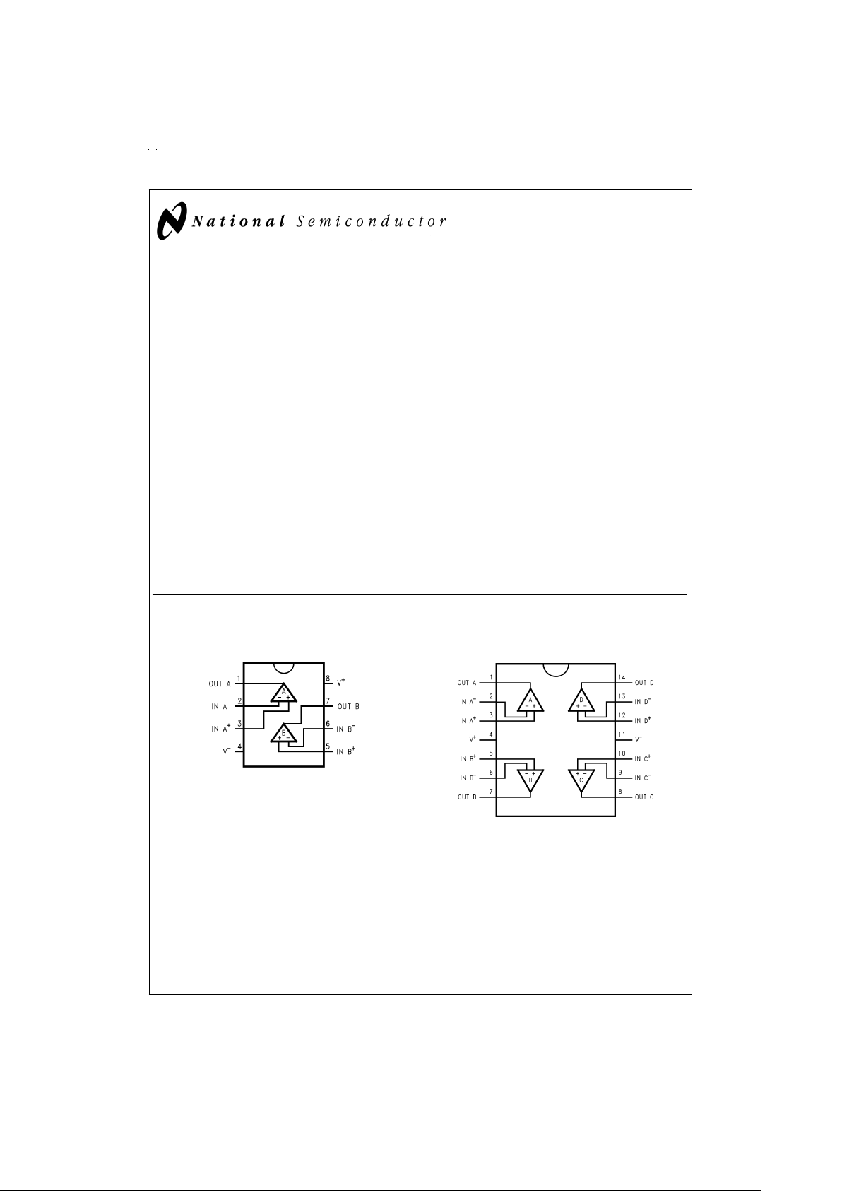
Connection Diagrams
8-Pin DIP/SO
DS012049-1
Top View
14-Pin DIP/SO
DS012049-2
Top View
October 1994
LMC6492 Dual/LMC6494 Quad CMOS Rail-to-Rail Input and Output Operational Amplifier
© 1999 National Semiconductor Corporation DS012049 www.national.com
Page 2
Ordering Information
Package
Temperature Range Transport
Media
NSC
Drawing
Extended −40˚C to +125˚C
8-Pin Small Outline LMC6492AEM Rails M08A
LMC6492BEM
LMC6492AEMX Tape and Reel
LMC6492BEMX
8-Pin Molded DIP LMC6492AEN Rails N08A
LMC6492BEN
14-Pin Small Outline LMC6494AEM Rails M14A
LMC6494BEM
LMC6494AEMX Tape and Reel
LMC6494BEMX
14-Pin Molded DIP LMC6494AEN Rails N14A
LMC6494BEN
www.national.com 2
Page 3
Absolute Maximum Ratings (Note 1)
If Military/Aerospace specified devices are required,
please contact the National Semiconductor Sales Office/
Distributors for availability and specifications.
ESD Tolerance (Note 2) 2000V
Differential Input Voltage
±
Supply Voltage
Voltage at Input/Output Pin (V
+
) + 0.3V, (V−) − 0.3V
Supply Voltage (V
+−V−
) 16V
Current at Input Pin
±
5mA
Current at Output Pin (Note 3)
±
30 mA
Current at Power Supply Pin 40 mA
Lead Temp. (Soldering, 10 sec.) 260˚C
Storage Temperature Range −65˚C to +150˚C
Junction Temperature (Note 4) 150˚C
Operating Conditions (Note 1)
Supply Voltage 2.5V ≤ V
+
≤ 15.5V
Junction Temperature Range
LMC6492AE, LMC6492BE −40˚C ≤ T
J
≤ +125˚C
LMC6494AE, LMC6494BE −40˚C ≤ T
J
≤ +125˚C
Thermal Resistance (θ
JA
)
N Package, 8-Pin Molded DIP 108˚C/W
M Package, 8-Pin Surface Mount 171˚C/W
N Package, 14-Pin Molded DIP 78˚C/W
M Package, 14-Pin Surface Mount 118˚C/W
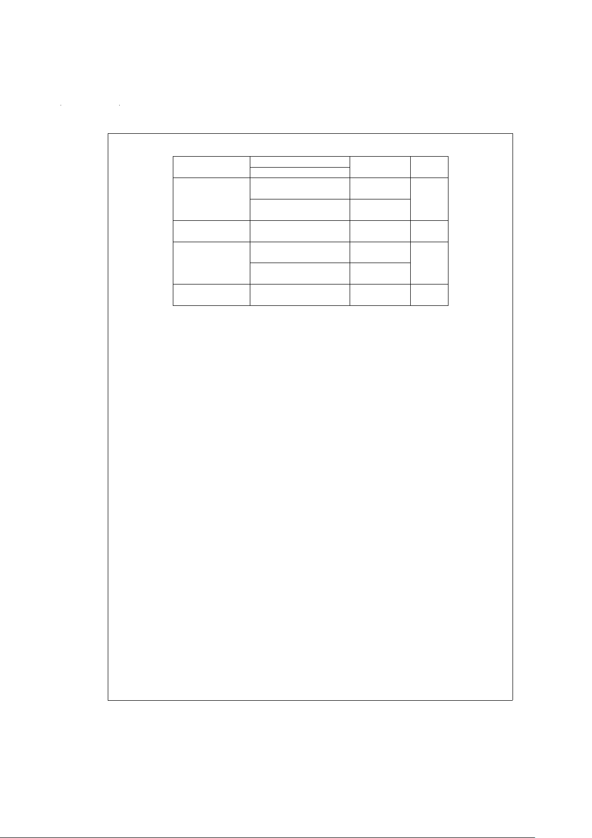
DC Electrical Characteristics
Unless otherwise specified, all limits guaranteed for T
J
=
25˚C, V
+
=
5V, V
−
=
0V, V
CM
=
V
O
=
V
+
/2 and R
L
>
1MΩ.Bold-
face limits apply at the temperature extremes
LMC6492AE LMC6492BE
Symbol Parameter Conditions Typ LMC6494AE LMC6494BE Units
(Note 5) Limit Limit
(Note 6) (Note 6)
V
OS
Input Offset Voltage 0.11 3.0 6.0 mV
3.8 6.8 max
TCV
OS
Input Offset Voltage 1.0 µV/˚C
Average Drift
I
B
Input Bias Current (Note 11) 0.15 200 200 pA max
I
OS
Input Offset Current (Note 11) 0.075 100 100 pA max
R
IN
Input Resistance
>
10 Tera Ω
C
IN
Common-Mode 3 pF
Input Capacitance
CMRR Common-Mode 0V ≤ V
CM
≤ 15V 82 65 63 dB
min
Rejection Ratio V
+
=
15V 60 58
0V ≤ V
CM
≤ 5V 82 65 63
60 58
+PSRR Positive Power Supply 5V ≤ V
+
≤ 15V, 82 65 63 dB
Rejection Ratio V
O
=
2.5V 60 58 min
−PSRR Negative Power Supply 0V ≤ V
−
≤ −10V, 82 65 63 dB
Rejection Ratio V
O
=
2.5V 60 58 min
V
CM
Input Common-Mode V
+
=
5V and 15V V
−
−0.3 −0.25 −0.25 V
Voltage Range For CMRR ≥ 50 dB 00max
V
+
+ 0.3 V++ 0.25 V++ 0.25 V
V
+
V
+
min
A
V
Large Signal Voltage Gain R
L
=
2kΩ: Sourcing 300 V/mV
(Note 7) Sinking 40 min
www.national.com3
Page 4
DC Electrical Characteristics (Continued)
Unless otherwise specified, all limits guaranteed for T
J
=
25˚C, V
+
=
5V, V
−
=
0V, V
CM
=
V
O
=
V
+
/2 and R
L
>
1MΩ.Bold-
face limits apply at the temperature extremes
LMC6492AE LMC6492BE
Symbol Parameter Conditions Typ LMC6494AE LMC6494BE Units
(Note 5) Limit Limit
(Note 6) (Note 6)
V
O
Output Swing V
+
=
5V 4.9 4.8 4.8 V
R
L
=
2kΩto V
+
/2 4.7 4.7 min
0.1 0.18 0.18 V
0.24 0.24 max
V
+
=
5V 4.7 4.5 4.5 V
R
L
=
600Ω to V
+
/2 4.24 4.24 min
0.3 0.5 0.5 V
0.65 0.65 max
V
+
=
15V 14.7 14.4 14.4 V
R
L
=
2kΩto V
+
/2 14.0 14.0 min
0.16 0.35 0.35 V
0.5 0.5 max
V
+
=
15V 14.1 13.4 13.4 V
R
L
=
600Ω to V
+
/2 13.0 13.0 min
0.5 1.0 1.0 V
1.5 1.5 max
I
SC
Output Short Circuit Current Sourcing, V
O
=
0V 25 16 16
mA
min
10 10
V
+
=
5V Sinking, V
O
=
5V 22 11 11
88
I
SC
Output Short Circuit Current Sourcing, V
O
=
0V 30 28 28
20 20
V
+
=
15V Sinking, V
O
=
5V
(Note 8)
30 30 30
22 22
I
S
Supply Current LMC6492 1.0 1.75 1.75 mA
V
+
=
+5V, V
O
=
V
+
/2 2.1 2.1 max
LMC6492 1.3 1.95 1.95 mA
V
+
=
+15V, V
O
=
V
+
/2 2.3 2.3 max
LMC6494 2.0 3.5 3.5 mA
V
+
=
+5V, V
O
=
V
+
/2 4.2 4.2 max
LMC6494 2.6 3.9 3.9 mA
V
+
=
+15V, V
O
=
V
+
/2 4.6 4.6 max
www.national.com 4
Page 5
AC Electrical Characteristics
Unless otherwise specified, all limits guaranteed for T
J
=
25˚C, V
+
=
5V, V
−
=
0V, V
CM
=
V
O
=
V
+
/2 and R
L
>
1MΩ.Bold-
face limits apply at the temperature extremes
LMC6492AE LMC6492BE
Symbol Parameter Conditions Typ LMC6494AE LMC6494BE Units
(Note 5) Limit Limit
(Note 6) (Note 6)
SR Slew Rate (Note 9) 1.3 0.7 0.7 Vµs min
0.5 0.5
GBW Gain-Bandwidth Product V
+
=
15V 1.5 MHz
φ
m
Phase Margin 50 Deg
G
m
Gain Margin 15 dB
Amp-to-Amp Isolation (Note 10) 150 dB
e
n
Input-Referred F=1 kHz
37
Voltage Noise V
CM
=
1V
i
n
Input-Referred F=1 kHz
0.06
Current Noise
T.H.D. Total Harmonic
Distortion
F=1 kHz, A
V
=
−2 0.01
%
R
L
=
10 kΩ,V
O
=
−4.1 V
PP
F=10 kHz, A
V
=
−2
R
L
=
10 kΩ,V
O
=
8.5 V
PP
0.01
V
+
=
10V
Note 1: Absolute Maximum Ratings indicate limits beyond which damage to the device may occur. Operating Ratings indicate conditions for which the device is intended to be functional, but specific performance is not guaranteed. For guaranteed specifications and the test conditions, see the Electrical Characteristics.
Note 2: Human body model, 1.5 kΩ in series with 100 pF.
Note 3: Applies to both single-supply and split-supply operation. Continuous short operation at elevated ambient temperature can result in exceeding the maximum
allowed junction temperature at 150˚C. Output currents in excess of
±
30 mA over long term may adversely affect reliability.
Note 4: The maximum power dissipation is a function of T
J(max)
, θJAand TA. The maximum allowable power dissipation at any ambient temperature is P
D
=
(T
J(max)
−TA)/θJA. All numbers apply for packages soldered directly into a PC board.
Note 5: Typical Values represent the most likely parametric norm.
Note 6: All limits are guaranteed by testing or statistical analysis.
Note 7: V
+
=
15V, V
CM
=
7.5V and R
L
connected to 7.5V. For Sourcing tests, 7.5V ≤ VO≤ 11.5V. For Sinking tests, 3.5V ≤ VO≤ 7.5V.
Note 8: Do not short circuit output to V
+
, when V+is greater than 13V or reliability will be adversely affected.
Note 9: V
+
=
15V. Connected as voltage follower with 10V step input. Number specified is the slower of the positive and negative slew rates.
Note 10: Input referred, V
+
=
15V and R
L
=
100 kΩ connected to 7.5V. Each amp excited in turn with 1 kHz to produce V
O
=
12 V
PP
.
Note 11: Guaranteed limits are dictated by tester limits and not device performance. Actual performance is reflected in the typical value.
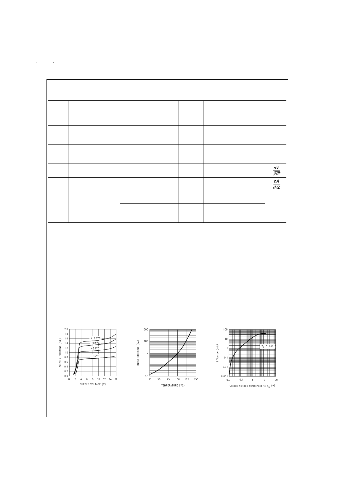
Typical Performance Characteristics V
S
=
+15V, Single Supply, T
A
=
25˚C unless otherwise
specified
Supply Current vs
Supply Voltage
DS012049-25
Input Current vs
Temperature
DS012049-26
Sourcing Current vs
Output Voltage
DS012049-27
www.national.com5
Page 6
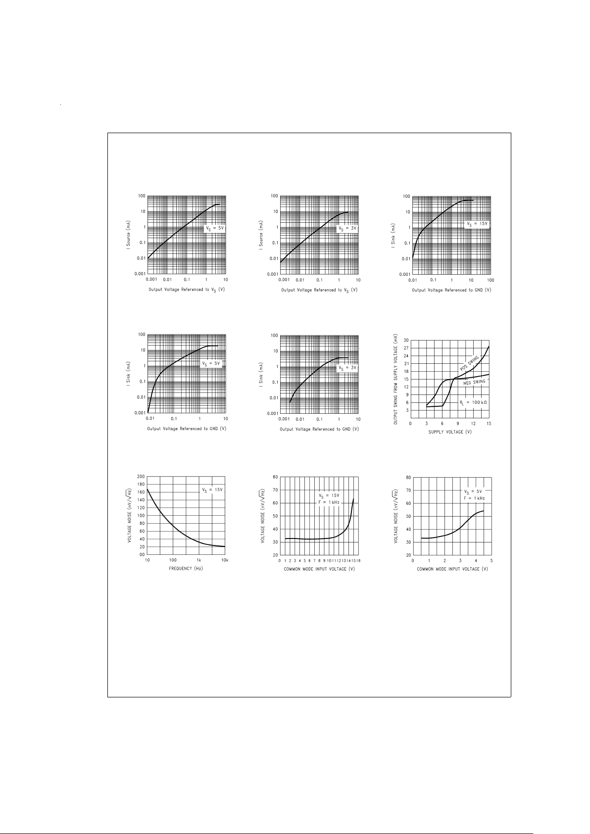
Typical Performance Characteristics V
S
=
+15V, Single Supply, T
A
=
25˚C unless otherwise
specified (Continued)
Sourcing Current vs
Output Voltage
DS012049-28
Sourcing Current vs
Output Voltage
DS012049-29
Sinking Current vs
Output Voltage
DS012049-30
Sinking Current vs
Output Voltage
DS012049-31
Sinking Current vs
Output Voltage
DS012049-32
Output Voltage Swing vs
Supply Voltage
DS012049-33
Input Voltage Noise
vs Frequency
DS012049-34
Input Voltage Noise
vs Input Voltage
DS012049-35
Input Voltage Noise
vs Input Voltage
DS012049-36
www.national.com 6
Page 7

Typical Performance Characteristics V
S
=
+15V, Single Supply, T
A
=
25˚C unless otherwise
specified (Continued)
Input Voltage Noise
vs Input Voltage
DS012049-37
Crosstalk Rejection
vs Frequency
DS012049-38
Crosstalk Rejection
vs Frequency
DS012049-39
Positive PSRR
vs Frequency
DS012049-40
Negative PSRR
vs Frequency
DS012049-41
CMRR vs
Frequency
DS012049-42
CMRR vs
Input Voltage
DS012049-43
CMRR vs
Input Voltage
DS012049-44
CMRR vs
Input Voltage
DS012049-45
www.national.com7
Page 8

Typical Performance Characteristics V
S
=
+15V, Single Supply, T
A
=
25˚C unless otherwise
specified (Continued)
∆V
OS
vs CMR
DS012049-46
∆V
OS
vs CMR
DS012049-47
Input Voltage vs
Output Voltage
DS012049-48
Input Voltage vs
Output Voltage
DS012049-49
Open Loop
Frequency Response
DS012049-50
Open Loop
Frequency Response
DS012049-51
Open Loop Frequency
Response vs Temperature
DS012049-52
Maximum Output Swing
vs Frequency
DS012049-53
Gain and Phase vs
Capacitive Load
DS012049-54
www.national.com 8
Page 9

Typical Performance Characteristics V
S
=
+15V, Single Supply, T
A
=
25˚C unless otherwise
specified (Continued)
Gain and Phase vs
Capacitive Load
DS012049-55
Open Loop Output
Impedance vs Frequency
DS012049-56
Open Loop Output
Impedance vs Frequency
DS012049-57
Slew Rate vs
Supply Voltage
DS012049-58
Non-Inverting Large
Signal Pulse Response
DS012049-59
Non-Inverting Large
Signal Pulse Response
DS012049-60
Non-Inverting Large
Signal Pulse Response
DS012049-61
Non-Inverting Small
Signal Pulse Response
DS012049-62
Non-Inverting Small
Signal Pulse Response
DS012049-63
www.national.com9
Page 10

Typical Performance Characteristics V
S
=
+15V, Single Supply, T
A
=
25˚C unless otherwise
specified (Continued)
Non-Inverting Small
Signal Pulse Response
DS012049-64
Inverting Large
Signal Pulse Response
DS012049-65
Inverting Large Signal
Pulse Response
DS012049-66
Inverting Large Signal
Pulse Response
DS012049-67
Inverting Small Signal
Pulse Response
DS012049-68
Inverting Small Signal
Pulse Response
DS012049-69
Inverting Small Signal
Pulse Response
DS012049-70
Stability vs
Capacitive Load
DS012049-71
Stability vs
Capacitive Load
DS012049-72
www.national.com 10
Page 11

Typical Performance Characteristics V
S
=
+15V, Single Supply, T
A
=
25˚C unless otherwise
specified (Continued)
Application Notes
Input Common-Mode Voltage Range
Unlike Bi-FET amplifier designs, the LMC6492/4 does not
exhibit phase inversion when an input voltage exceeds the
negative supply voltage.
Figure 1
shows an input voltage exceeding both supplies with no resulting phase inversion on
the output.
The absolute maximum input voltage is 300 mV beyond either supply rail at room temperature. Voltages greatly ex-
ceeding this absolute maximum rating, as in
Figure 2
, can
cause excessive current to flow in or out of the input pins
possibly affecting reliability.
Applications that exceed this rating must externally limit the
maximum input current to
±
5 mA with an input resistor (RI)
as shown in
Figure 3
.
Stability vs
Capacitive Load
DS012049-73
Stability vs
Capacitive Load
DS012049-74
Stability vs
Capacitive Load
DS012049-75
Stability vs
Capacitive Load
DS012049-76
DS012049-8
FIGURE 1. An Input Voltage Signal Exceeds the
LMC6492/4 Power Supply Voltages with
No Output Phase Inversion
DS012049-9
FIGURE 2. A±7.5V Input Signal Greatly
Exceeds the 5V Supply in
Figure 3
Causing
No Phase Inversion Due to R
I
www.national.com11
Page 12

Application Notes (Continued)
Rail-To-Rail Output
The approximate output resistance of the LMC6492/4 is
110Ω sourcing and 80Ω sinking at V
s
=
5V.Using the calculated output resistance, maximum output voltage swing can
be esitmated as a function of load.
Compensating for Input Capacitance
It is quite common to use large values of feedback resistance for amplifiers with ultra-low input current, like the
LMC6492/4.
Although the LMC6492/4 is highly stable over a wide range
of operating conditions, certain precautions must be met to
achieve the desired pulse response when a large feedback
resistor is used. Large feedback resistors with even small
values of input capacitance, due to transducers, photodiodes, and circuit board parasitics, reduce phase margins.
When high input impedances are demanded, guarding of the
LMC6492/4 is suggested. Guarding input lines will not only
reduce leakage, but lowers stray input capacitance as well.
(See
Printed-Circuit-Board Layout for High Impedance
Work
).
The effect of input capacitance can be compensated for by
adding a capacitor, C
f
, around the feedback resistors (as in
Figure 1
) such that:
or
R
1CIN
≤ R2C
f
Since it is often difficult to know the exact value of CIN,Cfcan
be experimentally adjusted so that the desired pulse response is achieved. Refer to the LMC660 and LMC662 for a
more detailed discussion on compensating for input
capacitance.
Capacitive Load Tolerance
All rail-to-rail output swing operational amplifiers have voltage gain in the output stage. A compensation capacitor is
normally included in this integrator stage. The frequency location of the dominant pole is affected by the resistive load
on the amplifier. Capacitive load driving capability can be optimized by using an appropriate resistive load in parallel with
the capacitive load (see Typical Curves).
Direct capacitive loading will reduce the phase margin of
many op-amps.A pole in the feedback loop is created by the
combination of the op-amp’s output impedance and the capacitive load. This pole induces phase lag at the unity-gain
crossover frequency of the amplifier resulting in either an oscillatory or underdamped pulse response. With a few external components, op amps can easily indirectly drive capacitive loads, as shown in
Figure 5
.
Printed-Circuit-Board Layout
for High-Impedance Work
It is generally recognized that any circuit which must operate
with less than 1000 pA of leakage current requires special
layout of the PC board. When one wishes to take advantage
of the ultra-low bias current of the LMC6492/4, typically
150 fA, it is essential to have an excellent layout. Fortunately, the techniques of obtaining low leakages are quite
simple. First, the user must not ignore the surface leakage of
the PC board, even though it may sometimes appear acceptably low, because under conditions of high humidity or dust
or contamination, the surface leakage will be appreciable.
To minimize the effect of any surface leakage, lay out a ring
of foil completely surrounding the LMC6492/4’s inputs and
the terminals of components connected to the op-amp’s inputs, as in
Figure 6
. Tohave a significant effect, guard rings
should be placed on both the top and bottom of the PC
board. This PC foil must then be connected to a voltage
which is at the same voltage as the amplifier inputs, since no
leakage current can flow between two points at the same potential. For example, a PC board trace-to-pad resistance of
10
12
Ω, which is normally considered a very large resistance,
could leak 5 pAif the trace were a 5V bus adjacent to the pad
of the input.
This would cause a 33 times degradation from the
LMC6492/4’s actual performance. If a guard ring is used and
held within 5 mV of the inputs, then the same resistance of
10
11
Ω will only cause 0.05 pA of leakage current. See
Figure
7
for typical connections of guard rings for standard op-amp
configurations.
DS012049-10
FIGURE 3. RIInput Current Protection for
Voltages Exceeding the Supply Voltages
DS012049-11
FIGURE 4. Cancelling the Effect of Input Capacitance
DS012049-12
FIGURE 5. LMC6492/4 Noninverting Amplifier,
Compensated to Handle Capacitive Loads
www.national.com 12
Page 13

Application Notes (Continued)
The designer should be aware that when it is inappropriate
to lay out a PC board for the sake of just a few circuits, there
is another technique which is even better than a guard ring
on a PC board: Don’t insert the amplifier’s input pin into the
board at all, but bend it up in the air and use only air as an insulator. Air is an excellent insulator. In this case you may
have to forego some of the advantages of PC board construction, but the advantages are sometimes well worth the
effort of using point-to-point up-in-the-air wiring. See
Figure
8
.
Application Circuits
DS012049-13
FIGURE 6. Examples of Guard
Ring in PC Board Layout
DS012049-14
Inverting Amplifier
DS012049-15
Non-Inverting Amplifier
DS012049-16
Follower
FIGURE 7. Typical Connections of Guard Rings
DS012049-17
(Input pins are lifted out of PC board and soldered directly to components.
All other pins connected to PC board).
FIGURE 8. Air Wiring
DC Summing Amplifier (V
IN
≥ 0VDCand VO≥ V
DC
DS012049-18
Where: V
0
=
V
1+V2−V3–V4
(V1+V2≥(V3+V4) to keep V
0
>
0V
DC
www.national.com13
Page 14

Application Circuits (Continued)
This low-pass filter circuit can be used as an anti-aliasing filter with the same supply as the A/D converter. Filter designs
can also take advantage of the LMC6492/4 ultra-low input
current. The ultra-low input current yields negligible offset error even when large value resistors are used. This in turn allows the use of smaller valued capacitors which take less
board space and cost less.
Dielectric absorption and leakage is minimized by using a
polystyrene or polypropylene hold capacitor. The droop rate
is primarily determined by the value of C
H
and diode leakage
current. Select low-leakage current diodes to minimize
drooping.
In a manifold absolute pressure sensor application, a strain
gauge is mounted on the intake manifold in the engine unit.
Manifold pressure causes the sensing resistors, R1, R2, R3
High Input Z, DC Differential Amplifier
DS012049-19
For
(CMRR depends on this resistor ratio match)
As shown: V
O
=
2(V
2−V1
)
Photo Voltaic-Cell Amplifier
DS012049-20
Instrumentation Amplifier
DS012049-21
If R1=R5, R3=R6, and R4=R7; then
∴
AV≈ 100 for circuit shown (R
2
=
9.3k).
Rail-to-Rail Single Supply Low Pass Filter
DS012049-22
Low Voltage Peak Detector with Rail-to-Rail Peak
Capture Range
DS012049-23
Pressure Sensor
DS012049-24
R
f
=
Rx
R
f
>>
R1, R2, R3, and R4
www.national.com 14
Page 15

Application Circuits (Continued)
and R4 to change. The resistors change in a way such that
R2 and R4 increase by the same amount R1 and R3 decrease. This causes a differential voltage between the input
of the amplifier. The gain of the amplifier is adjusted by R
f
.
Spice Macromodel
A spice macromodel is available for the LMC6492/4. This
model includes accurate simulation of:
•
Input common-model voltage range
•
Frequency and transient response
•
GBW dependence on loading conditions
•
Quiescent and dynamic supply current
•
Output swing dependence on loading conditions
and many other characteristics as listed on the macromodel
disk.
Contact your local National Semiconductor sales office to
obtain an operational amplifier spice model library disk.
www.national.com15
Page 16

Physical Dimensions inches (millimeters) unless otherwise noted
8-Pin Small Outline Package
Order Number LMC6492AEM or LMC6492BEM
NS Package Number M08A
14-Pin Small Outline Package
Order Number LMC6494AEM or LMC6494BEM
NS Package Number M14A
www.national.com 16
Page 17

Physical Dimensions inches (millimeters) unless otherwise noted (Continued)
8-Lead (0.300" Wide) Molded Dual-In-Line Package
Order Number LMC6492AEN or LMC6492BEN
NS Package Number N08A
14-Lead Molded Dual-In-Line Package
Order Number LMC6494AEN or LMC6494BEN
NS Package Number N14A
www.national.com17
Page 18

LIFE SUPPORT POLICY
NATIONAL’S PRODUCTS ARE NOT AUTHORIZED FOR USE AS CRITICAL COMPONENTS IN LIFE SUPPORT DEVICES OR SYSTEMS WITHOUT THE EXPRESS WRITTEN APPROVAL OF THE PRESIDENT OF NATIONAL SEMICONDUCTOR CORPORATION. As used herein:
1. Life support devices or systems are devices or systems which, (a) are intended for surgical implant into
the body, or (b) support or sustain life, and whose failure to perform when properly used in accordance
with instructions for use provided in the labeling, can
be reasonably expected to result in a significant injury
to the user.
2. A critical component is any component of a life support
device or system whose failure to perform can be reasonably expected to cause the failure of the life support
device or system, or to affect its safety or effectiveness.
National Semiconductor
Corporation
Americas
Tel: 1-800-272-9959
Fax: 1-800-737-7018
Email: support@nsc.com
www.national.com
National Semiconductor
Europe
Fax: +49 (0) 1 80-530 85 86
Email: europe.support@nsc.com
Deutsch Tel: +49 (0) 1 80-530 85 85
English Tel: +49 (0) 1 80-532 78 32
Français Tel: +49 (0) 1 80-532 93 58
Italiano Tel: +49 (0) 1 80-534 16 80
National Semiconductor
Asia Pacific Customer
Response Group
Tel: 65-2544466
Fax: 65-2504466
Email: sea.support@nsc.com
National Semiconductor
Japan Ltd.
Tel: 81-3-5639-7560
Fax: 81-3-5639-7507
LMC6492 Dual/LMC6494 Quad CMOS Rail-to-Rail Input and Output Operational Amplifier
National does not assume any responsibility for use of any circuitry described, no circuit patent licenses are implied and National reserves the right at any time without notice to change said circuitry and specifications.
 Loading...