

Page 1
LMC6035/LMC6036
Low Power 2.7V Single Supply CMOS Operational
Amplifiers
LMC6035/LMC6036 Low Power 2.7V Single Supply CMOS Operational Amplifiers
January 2000
General Description
The LMC6035/6 is an economical, low voltage op amp capable of rail-to-rail output swing into loads of 600Ω.
LMC6035 is available in a chip sized package (8-Bump micro SMD) using National’s micro SMD package technology.
Both allow for single supply operation and are guaranteed
for 2.7V, 3V, 5V and15Vsupply voltage. The 2.7 supply voltage corresponds to the End-of-Life voltage (0.9V/cell) for
three NiCd or NiMH batteries in series, making the
LMC6035/6 well suited for portable and rechargeable systems. It also features a well behaved decrease in its specifications at supply voltages below its guaranteed 2.7V operation. This provides a “comfort zone” for adequate operation
at voltages significantly below 2.7V. Its ultra low input currents (I
plication, because it allows the use of higher resistor values
and lower capacitor values. In addition, the drive capability of
the LMC6035/6 gives these op amps a broad range of applications for low voltage systems.
) makes it well suited for low power active filter ap-
IN
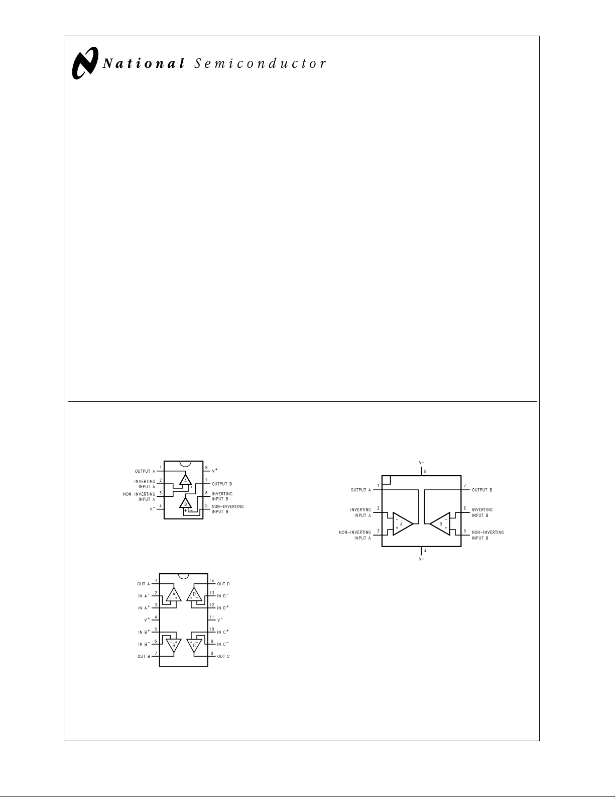
Connection Diagrams
8-Pin SO/MSOP
Features
(Typical Unless Otherwise Noted)
n LMC6035 in micro SMD Package
n Guaranteed 2.7V, 3V, 5V and 15V Performance
n Specified for 2 kΩ and 600Ω Loads
n Wide Operating Range: 2.0V to 15.5V
n Ultra Low Input Current: 20 fA
n Rail-to-Rail Output Swing
@
600Ω: 200 mV from either rail at 2.7V
@
100 kΩ: 5 mV from either rail at 2.7V
n High Voltage Gain: 126dB
n Wide Input Common-Mode Voltage Range
-0.1V to 2.3V at Vs = 2.7V
n Low Distortion: 0.01%at 10 kHz
Applications
n Filters
n High Impedance Buffer or Preamplifier
n Battery Powered Electronics
n Medical Instrumentation
8-Bump micro SMD
DS012830-1
Top View
14-Pin SO/TSSOP
Top View
(Bump Side Down)
DS012830-2
Top View
© 2000 National Semiconductor Corporation DS012830 www.national.com
DS012830-65
Page 2
Ordering Information
LMC6035/LMC6036
Package Temperature
Range
Industrial
−40˚C to +85˚C
8-pin Small Outline (SO) LMC6035IM Rails
LMC6035IMX 2.5k Units
8-pin Mini Small Outline
(MSOP)
14-pin Small Outline (SO) LMC6036IM Rails
14-pin Thin Shrink Small
Outline (TSSOP)
8-Bump micro SMD LMC6035IBP 250 Units
LMC6035IMM 1k Units Tape
LMC6035IMMX 3.5k Units
LMC6036IMX 2.5k Units
LMC6036IMT Rails
LMC6036IMTX 2.5k Units
LMC6035IBPX 3k Units Tape
Transport
Media
Tape and
Reel
and Reel
Tape and
Reel
Tape and
Reel
Tape and
Reel
Tape and
Reel
and Reel
NSC
Drawing
M08A
MUA08A
M14A
MTC14
BPA08FFB
www.national.com 2
Page 3
LMC6035/LMC6036
Absolute Maximum Ratings (Note 1)
If Military/Aerospace specified devices are required,
please contact the National Semiconductor Sales Office/
Distributors for availability and specifications.
ESD Tolerance (Note 2)
Human Body Model 3000V
Machine Model 300V
±
Differential Input Voltage
Supply Voltage (V
+−V−
Output Short Circuit to V
Output Short Circuit to V
) 16V
+
−
Supply Voltage
(Note 8)
(Note 3)
Lead Temperature (soldering, 10 sec.) 260˚C
±
Current at Output Pin
Current at Input Pin
18 mA
±
5mA
Current at Power Supply Pin 35 mA
DC Electrical Characteristics
Unless otherwise specified, all limits guaranteed for T
Boldface limits apply at the temperature extremes.
Symbol Parameter Conditions
V
OS
TCV
OS
Input Offset Voltage 0.5 5 mV
Input Offset Voltage 2.3 µV/˚C
Average Drift
I
IN
I
OS
R
IN
Input Current (Note 11) 0.02 pA
Input Offset Current (Note 11) 0.01 pA
Input Resistance
CMRR Common Mode 0.7V ≤ V
+
Rejection Ratio V
=
+PSRR Positive Power Supply 5V ≤ V
Rejection Ratio V
O
−PSRR Negative Power Supply 0V ≤ V
Rejection Ratio V
V
CM
Input Common-Mode V
O
+
=
Voltage Range For CMRR ≥ 40 dB 0.5 max
+
=
V
For CMRR ≥ 40 dB 0.3 max
+
=
V
For CMRR ≥ 50 dB 0.0 max
+
=
V
For CMRR ≥ 50 dB 0.0 max
=
25˚C, V
J
≤ 12.7V 96 63 dB
CM
15V 60 min
+
≤ 15V, 93 63 dB
=
2.5V 60 min
−
≤ −10V 97 74 dB
2.5V, V
+
=
5V 70 min
=
2.7V −0.1 0.3 V
3V −0.3 0.1 V
5V −0.5 −0.2 V
15V −0.5 −0.2 V
Storage Temperature Range −65˚C to +150˚C
Junction Temperature (Note 4) 150˚C
Operating Ratings (Note 1)
Supply Voltage 2.0V to 15.5V
Temperature Range
L
≤ +85˚C
J
>
1MΩ.
UnitsLMC6036I
LMC6035I and LMC6036I −40˚C ≤ T
Thermal Resistance (θ
)
JA
MSOP, 8-pin Mini Surface Mount 230˚C/W
M Package, 8-pin Surface Mount 175˚C/W
M Package, 14-pin Surface Mount 127˚C/W
MTC Package, 14-pin TSSOP 137˚C/W
BP, 8-Bump micro SMD Package 220˚C/W
+
=
2.7V, V
−
=
0V, V
CM
=
1.0V, V
=
1.35V and R
O
LMC6035I
Typ
(Note 5)
Limit (Note 6)
6 max
90 max
45 max
>
10 Tera Ω
2.3 2.0 V
1.7 min
2.6 2.3 V
2.0 min
4.5 4.2 V
3.9 min
14.4 14.0 V
13.7 min
www.national.com3
Page 4
DC Electrical Characteristics (Continued)
Unless otherwise specified, all limits guaranteed for T
Boldface limits apply at the temperature extremes.
Symbol Parameter Conditions
LMC6035/LMC6036
A
V
Large Signal Voltage Gain R
L
(Note 7) 75 min
=
R
L
V
O
I
O
I
S
Output Swing V
Output Current V
Supply Current LMC6035 for Both Amplifiers 0.65 1.6 mA
+
R
L
+
V
R
L
+
V
R
L
+
V
R
L
O
V
O
V
O
LMC6036 for All Four Amplifiers 1.3 2.7 mA
V
O
=
J
=
600Ω Sourcing 1000 100 V/mV
2kΩ Sourcing 2000 V/mV
=
2.7V 2.5 2.0 V
=
600Ω to 1.35V 1.8 min
=
2.7V 2.62 2.4 V
=
2kΩto 1.35V 2.2 min
=
15V 14.5 13.5 V
=
600Ω to 7.5V 13.0 min
=
15V 14.8 14.2 V
=
2kΩto 7.5V 13.5 min
=
0V Sourcing 8 4 mA
=
2.7V Sinking 5 3 mA
=
1.35V 1.9 max
=
1.35V 3.0 max
25˚C, V
+
=
2.7V, V
−
=
0V, V
CM
=
1.0V, V
=
1.35V and R
O
L
>
1MΩ.
LMC6035I
Typ
(Note 5)
UnitsLMC6036I
Limit (Note 6)
Sinking 250 25 V/mV
20 min
Sinking 500 V/mV
0.2 0.5 V
0.7 max
0.07 0.2 V
0.4 max
0.36 1.25 V
1.50 max
0.12 0.4 V
0.5 max
3 min
2 min
www.national.com 4
Page 5
LMC6035/LMC6036
AC Electrical Characteristics
25˚C, V
+
=
Unless otherwise specified, all limits guaranteed for T
1MΩ.Boldface limits apply at the temperature extremes.
=
J
Symbol Parameter Conditions Typ Units
SR Slew Rate (Note 9) 1.5 V/µs
+
GBW Gain Bandwidth Product V
θ
m
G
m
Phase Margin 48 ˚
Gain Margin 17 dB
=
15V 1.4 MHz
Amp-to-Amp Isolation (Note 10) 130 dB
e
n
i
n
Input-Referred Voltage Noise f=1 kHz 27
=
V
CM
1V
Input Referred Current Noise f=1 kHz 0.2
THD Total Harmonic Distortion f=10 kHz, A
=
R
2kΩ,V
L
+
=
V
10V
Note 1: Absolute Maximum Ratings indicate limits beyond which damage to the device may occur. Operating Ratings indicate conditions for which the device is intended to be functional, but specific performance is not guaranteed. For guaranteed specifications and the test conditions, see the Electrical Characteristics.
Note 2: Human body model, 1.5 kΩ in series with 100 pF.
Note 3: Applies to both single-supply and split-supply operation. Continuous short circuit operation at elevated ambient temperature can result in exceeding the
maximum allowed junction temperature of 150˚C. Output currents in excess of 30 mA over long term may adversely affect reliabilty.
Note 4: Themaximum power dissipation is a function of T
−TA)/θJA. All numbers apply for packages soldered directly onto a PC board with no air flow.
Note 5: Typical Values represent the most likely parametric norm or one sigma value.
Note 6: All limits are guaranteed by testing or statistical analysis.
Note 7: V
Note 8: Do not short circuit output to V
Note 9: V
Note 10: Input referred, V
Note 11: Guaranteed by design.
+
=
15V, V
+
=
15V. Connected as voltage follower with 10V step input. Number specified is the slower of the positive and negative slew rates.
CM
=
7.5V and R
+
=
15V and R
connected to 7.5V. For Sourcing tests, 7.5V ≤ VO≤ 11.5V. For Sinking tests, 3.5V ≤ VO≤ 7.5V.
L
+
when V+is greater than 13V or reliability will be adversely affected.
=
100 kΩ connected to 7.5V. Each amp excited in turn with 1 kHz to produce V
L
, θJA, and TA. The maximum allowable power dissipation at any ambient temperature is P
J(max)
2.7V, V
V
O
−
=
0V, V
CM
=
1.0V, V
=
1.35V and R
O
>
L
(Note 5)
=
−10
=
8V
PP
0.01
=
.
12 V
O
PP
%
=
(T
D
J(max)
www.national.com5
Page 6
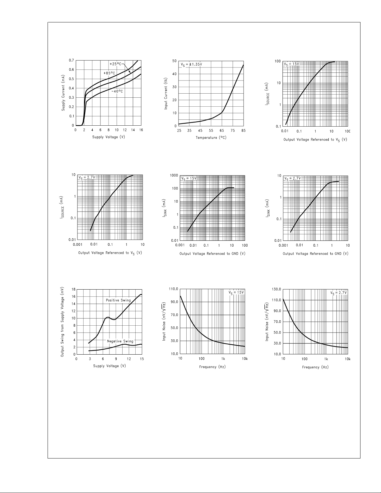
Typical Performance Characteristics Unless otherwise specified, V
=
2.7V, single supply, T
S
=
25˚C
A
Supply Current vs
Supply Voltage (Per Amplifier)
LMC6035/LMC6036
Sourcing Current vs
Output Voltage
DS012830-52
Input Current vs
Temperature
Sinking Current vs
Output Voltage
DS012830-53
Sourcing Current vs
Output Voltage
DS012830-54
Sinking Current vs
Output Voltage
Output Voltage Swing vs
Supply Voltage
DS012830-55
DS012830-58
Input Noise vs
Frequency
DS012830-56
DS012830-59
DS012830-57
Input Noise vs
Frequency
DS012830-60
www.national.com 6
Page 7

LMC6035/LMC6036
Typical Performance Characteristics Unless otherwise specified, V
25˚C (Continued)
Amp to Amp Isolation vs
Frequency
DS012830-61
−PSRR vs Frequency
Amp to Amp Isolation vs
Frequency
CMRR vs Frequency
+PSRR vs Frequency
DS012830-62
CMRR vs Input Voltage
=
2.7V, single supply, T
S
=
A
DS012830-32
CMRR vs Input Voltage
DS012830-33
DS012830-36
Input Voltage vs
Output Voltage
DS012830-34
DS012830-14
DS012830-35
Input Voltage vs
Output Voltage
DS012830-15
www.national.com7
Page 8

Typical Performance Characteristics Unless otherwise specified, V
25˚C (Continued)
=
2.7V, single supply, T
S
=
A
Frequency Response
vs Temperature
LMC6035/LMC6036
Gain and Phase vs
Capacitive Load
DS012830-16
Frequency Response
vs Temperature
Slew Rate vs
Supply Voltage
DS012830-17
Gain and Phase vs
Capacitive Load
DS012830-18
Non-Inverting
Large Signal Response
Non-Inverting
Large Signal Response
DS012830-19
DS012830-21
Non-Inverting
Large Signal Response
DS012830-37
DS012830-22
DS012830-20
Non-Inverting
Small Signal Response
DS012830-23
www.national.com 8
Page 9

LMC6035/LMC6036
Typical Performance Characteristics Unless otherwise specified, V
25˚C (Continued)
Non-Inverting
Small Signal Response
DS012830-24
Inverting Large
Signal Response
Non-Inverting
Large Signal Response
Inverting Large
Signal Response
Inverting Large
Signal Response
DS012830-25
Inverting Small
Signal Response
=
2.7V, single supply, T
S
=
A
DS012830-26
Inverting Small
Signal Response
DS012830-27
DS012830-30
Inverting Small
Signal Response
DS012830-28
DS012830-31
DS012830-29
Stability vs
Capacitive Load
DS012830-38
www.national.com9
Page 10

Typical Performance Characteristics Unless otherwise specified, V
25˚C (Continued)
=
2.7V, single supply, T
S
=
A
Stability vs
Capacitive Load
LMC6035/LMC6036
Stability vs
Capacitive Load
DS012830-39
Stability vs
Capacitive Load
Stability vs
Capacitive Load
DS012830-40
Stability vs
Capacitive Load
DS012830-41
DS012830-42
DS012830-43
www.national.com 10
Page 11

1.0 Application Notes
1.1 Background
The LMC6035/6 is exceptionally well suited for low voltage
applications. A desirable feature that the LMC6035/6 brings
to low voltage applications is its output drive capability—a
hallmark for National’s CMOS amplifiers. The circuit of
ure 1
illustrates the drive capability of the LMC6035/6 at 3V
of supply. It is a differential output driver for a one-to-one audio transformer, like those used for isolating ground from the
telephone lines. The transformer (T1) loads the op amps
with about 600Ω of AC load, at 1 kHz. Capacitor C1 functions
to block DC from the low winding resistance of T1. Although
the value of C1 is relatively high, its load reactance (Xc) is
negligible compared to inductive reactance (X
) of T1.
I
Fig-
DS012830-45
FIGURE 2. Output Swing Performance of
the LMC6035 per the Circuit of
Figure 1
LMC6035/LMC6036
DS012830-44
FIGURE 1. Differential Driver
The circuit in
Figure 1
consists of one input signal and two
output signals. U1Aamplifies the input with an inverting gain
of −2, while the U1B amplifies the input with a noninverting
gain of +2. Since the two outputs are 180˚ out of phase with
each other, the gain across the differential output is 4. As the
differential output swings between the supply rails, one of
the op amps sources the current to the load, while the other
op amp sinks the current.
How good a CMOS op amp can sink or source a current is
an important factor in determining its output swing capability.
The output stage of the LMC6035/6— like many op
amps—sources and sinks output current through two
complementary transistors in series. This “totem pole” arrangement translates to a channel resistance (R
dson
) at each
supply rail which acts to limit the output swing. Most CMOS
op amps are able to swing the outputs very close to the
rails—except, however, under the difficult conditions of low
supply voltage and heavy load. The LMC6035/6 exhibits exceptional output swing capability under these conditions.
The scope photos of
Figure 2
and
Figure 3
represent measurements taken directly at the output (relative to GND) of
U1A, in
bility of the LMC6035, while
Figure 1.Figure 2
illustrates the output swing capa-
Figure 3
provides a benchmark
comparison. (The benchmark op amp is another low voltage
(3V) op amp manufactured by one of our reputable
competitors.)
DS012830-46
FIGURE 3. Output Swing Performance of
Benchmark Op Amp per the Circuit of
Figure 1
Notice the superior drive capability of LMC6035 when compared with the benchmark measurement—even though the
benchmark op amp uses twice the supply current.
Not only does the LMC6035/6 provide excellent output swing
capability at low supply voltages, it also maintains high open
loop gain (A
) with heavy loads. To illustrate this, the
VOL
LMC6035 and the benchmark op amp were compared for
their distortion performance in the circuit of
graph of
Figure 4
shows this comparison. The y-axis repre-
Figure 1
. The
sents percent Total Harmonic Distortion (THD plus noise)
across the loaded secondary of T1. The x-axis represents
the input amplitude of a 1 kHz sine wave. (Note that T1 loses
about 20%of the voltage to the voltage divider of R
(600Ω)
L
and T1’s winding resistances—a performance deficiency of
the transformer.)
www.national.com11
Page 12

1.0 Application Notes (Continued)
LMC6035/LMC6036
FIGURE 4. THD+Noise Performance of LMC6035 and
“Benchmark” per Circuit of
Figure 4
shows the superior distortion performance of
LMC6035/6 over that of the benchmark op amp. The heavy
loading of the circuit causes the A
to drop significantly which causes increased distortion.
Figure 1
of the benchmark part
VOL
DS012830-47
1.2.1.1 Low-Pass Frequency Scaling Procedure
The actual component values represented in bold of
Figure 5
were obtained with the following scaling procedure:
1. First determine the frequency scaling factor (FSF) for
the desired cutoff frequency. Choosing f
at 3 kHz, pro-
c
vides the following FSF computation:
FSF=2π x 3 kHz
(desired cutoff freq.)
=
18.84 x 10
3
2. Then divide all of the normalized capacitor values by the
FSF as follows:
C1’=C
(Normalized)
C1’=0.707/18.84 x 10
C2’=1.414/18.84 x 10
/FSF
3
=
37.93 x 10
3
=
75.05 x 10
−6
−6
(C1’ and C2’: prior to impedance scaling)
3. Last, choose an impedance scaling factor (Z). This Z
factor can be calculated from a standard value for C2.
Then Z can be used to determine the remaining component values as follows:
Z=C2’/C2
(chosen)
=
C1=C1’/Z=37.93 x 10
75.05 x 10
−6
/6.8 nF=8.4k
−6
/8.4k=4.52 nF
(Standard capacitor value chosen for C1 is 4.7 nF )
R1=R1
R2=R2
(normalized)
(normalized)
xZ=1Ωx 8.4k=8.4 kΩ
xZ=1Ωx 8.4k=8.4 kΩ
(Standard value chosen for R1 and R2 is 8.45 kΩ )
1.2.2 High Pass Active Filter
The previous low-pass filter circuit of
high-pass active filter per
Figure 6
Figure 5
.
converts to a
1.2 APPLICATION CIRCUITS
1.2.1 Low-Pass Active Filter
A common application for low voltage systems would be active filters, in cordless and cellular phones for example. The
ultra low input currents (I
) of the LMC6035/6 makes it well
IN
suited for low power active filter applications, because it allows the use of higher resistor values and lower capacitor
values. This reduces power consumption and space.
Figure 5
shows a low pass, active filter with a Butterworth
(maximally flat) frequency response. Its topology is a Sallen
and Key filter with unity gain. Note the normalized component values in parenthesis which are obtainable from standard filter design handbooks. These values providea1Hz
cutoff frequency, but they can be easily scaled for a desired
cutoff frequency (f
). The bold component values of
c
Figure 5
provide a cutoff frequency of 3 kHz. An example of the scaling procedure follows
Figure 5
.
DS012830-48
FIGURE 5. 2-Pole, 3 kHz, Active, Sallen and Key,
Lowpass Filter with Butterworth Response
DS012830-49
FIGURE 6. 2 Pole, 300 Hz, Sallen and Key,
High-Pass Filter
1.2.2.1 High-Pass Frequency Scaling Procedure
Choose a standard capacitor value and scale the impedances in the circuit according to the desired cutoff frequency
(300 Hz) as follows:
C=C1=C2
Z=1 Farad/C
=
1 Farad/6.8 nF x2πx 300 Hz=78.05k
R1=ZxR1
(normalized)
x2πx (desired cutoff freq.)
(chosen)
=
78.05k x (1/0.707)=110.4 kΩ
(Standard value chosen for R1 is 110 kΩ )
R2=ZxR2
(normalized)
=
78.05k x (1/1.414)=55.2 kΩ
(Standard value chosen for R1 is 54.9 kΩ )
1.2.3 Dual Amplifier Bandpass Filter
The dual amplifier bandpass (DABP) filter features the ability
to independently adjust f
pologies, the f
and Q adjustments interact with each other.
c
and Q. In most other bandpass to-
c
The DABP filter also offers both low sensitivity to component
values and high Qs. The following application of
Figure 7
provides a 1 kHz center frequency andaQof100.
,
www.national.com 12
Page 13

1.0 Application Notes (Continued)
DS012830-50
FIGURE 7. 2 Pole, 1 kHz Active, Bandpass Filter
1.2.3.1 DABP Component Selection Procedure
Component selection for the DABP filter is performed as follows:
1. First choose a center frequency (f
component values that were obtained from the following
computation for a center frequency of 1 kHz.
R2=R3=1/(2 πf
Given: f
=
c
C)
c
1 kHz and C
R2=R3=1/(2π x 3 kHz x 6.8 nF)=23.4 kΩ
(Chosen standard value is 23.7 kΩ )
2. Then compute R1 for a desired Q (f
R1=Q x R2.
ChoosingaQof100,
R1=100 x 23.7 kΩ=2.37 MΩ.
(chosen)
).
Figure 7
c
=
6.8 nF
/BW) as follows:
c
represents
the user must not ignore the surface leakage of the PC
board, even though it may at times appear acceptably low.
Under conditions of high humidity, dust or contamination, the
surface leakage will be appreciable.
To minimize the effect of any surface leakage, lay out a ring
of foil completely surrounding the LMC6035 or LMC6036 inputs and the terminals of capacitors, diodes, conductors, resistors, relay terminals, etc. connected to the op amp’s inputs. See
Figure 8
. To have a significant effect, guard rings
should be placed on both the top and bottom of the PC
board. This PC foil must then be connected to a voltage
which is at the same voltage as the amplifier inputs, since no
leakage current can flow between two points at the same potential. For example, a PC board trace-to-pad resistance of
12
10
Ω, which is normally considered a very large resistance,
could leak 5 pA if the trace were a 5V bus adjacent to the pad
of an input. This would cause a 100 times degradation from
the amplifiers actual performance. However, if a guard ring is
held within 5 mV of the inputs, then even a resistance of
11
10
Ω would cause only 0.05 pA of leakage current, or perhaps a minor (2:1) degradation of the amplifier’s performance. See
Figure 9a, b, c
for typical connections of guard
rings for standard op amp configurations. If both inputs are
active and at high impedance, the guard can be tied to
ground and still provide some protection; see
Figure 9 d
.
LMC6035/LMC6036
1.3 PRINTED-CIRCUIT-BOARD LAYOUT
FOR HIGH-IMPEDANCE WORK
It is generally recognized that any circuit which must operate
<
with
1000 pA of leakage current requires special layout of
the PC board. If one wishes to take advantage of the
ultra-low bias current of the LMC6035/6, typically
<
0.04 pA,
it is essential to have an excellent layout. Fortunately, the
techniques for obtaining low leakages are quite simple. First,
DS012830-7
FIGURE 8. Example, using the LMC6036
of Guard Ring in P.C. Board Layout
www.national.com13
Page 14

1.0 Application Notes (Continued)
LMC6035/LMC6036
(a) Inverting Amplifier
(b) Non-Inverting Amplifier
DS012830-10
(c) Follower
DS012830-8
DS012830-9
FIGURE 9. Guard Ring Connections
1.3.1 CAPACITIVE LOAD TOLERANCE
Like many other op amps, the LMC6035/6 may oscillate
when its applied load appears capacitive. The threshold of
oscillation varies both with load and circuit gain. The configuration most sensitive to oscillation is a unity-gain follower.
See the Typical Performance Characteristics.
The load capacitance interacts with the op amp’s output resistance to create an additional pole. If this pole frequency is
sufficiently low, it will degrade the op amp’s phase margin so
that the amplifier is no longer stable at low gains. As shown
in
Figure 10
, the addition of a small resistor (50Ω–100Ω)in
series with the op amp’s output, and a capacitor (5 pF–10
pF) from inverting input to output pins, returns the phase
margin to a safe value without interfering with
lower-frequency circuit operation. Thus, larger values of capacitance can be tolerated without oscillation. Note that in all
cases, the output will ring heavily when the load capacitance
is near the threshold for oscillation.
1.4 Micro SMD Considerations
Contrary to what might be guessed, the micro SMD package
does not follow the trend of smaller packages having higher
thermal resistance. LMC6035 in micro SMD has thermal resistance of 220˚C/W compared to 230˚C/W in MSOP. Even
when driving a 600Ω load and operating from
±
7.5V supplies, the maximum temperature raise will be under 4.5˚C.
For application information specific to micro SMD, see Application note AN-1112.
DS012830-11
(d) Howland Current Pump
DS012830-5
FIGURE 10. Rx, Cx Improve Capacitive Load Tolerance
Capacitive load driving capability is enhanced by using a pull
up resistor to V
+
(
Figure 11
). Typically a pull up resistor conducting 500 µA or more will significantly improve capacitive
load responses. The value of the pull up resistor must be determined based on the current sinking capability of the amplifier with respect to the desired output swing. Open loop gain
of the amplifier can also be affected by the pull up resistor
(see Electrical Characteristics).
DS012830-6
FIGURE 11. Compensating for Large
Capacitive Loads with a Pull Up Resistor
www.national.com 14
Page 15

Physical Dimensions inches (millimeters) unless otherwise noted
LMC6035/LMC6036
8-Lead (0.150" Wide) Molded
Small Outline Package, JEDEC
NS Package Number M08A
www.national.com15
Page 16

Physical Dimensions inches (millimeters) unless otherwise noted (Continued)
LMC6035/LMC6036
8-Lead (0.150" Wide) Molded
Mini Small Outline Package, JEDEC
NS Package Number MUA08A
www.national.com 16
Page 17

Physical Dimensions inches (millimeters) unless otherwise noted (Continued)
LMC6035/LMC6036
14-Lead (0.150" Wide) Molded
Small Outline Package, JEDEC
NS Package Number M14A
www.national.com17
Page 18

Physical Dimensions inches (millimeters) unless otherwise noted (Continued)
LMC6035/LMC6036
14-Pin TSSOP
NS Package Number MTC14
www.national.com 18
Page 19

Physical Dimensions inches (millimeters) unless otherwise noted (Continued)
LMC6035/LMC6036
NOTE: UNLESS OTHERWISE SPECIFIED.
1. EPOXY COATING.
2. 63Sn/37Pb EUTECTIC BUMP.
3. RECOMMEND NON-SOLDER MASK DEFINED LANDING PAD.
4. PIN 1 IS ESTABLISHED BY LOWER LEFT CORNER WITH RESPECT TO TEXT ORIENTATION PINS ARE NUMBERED
COUNTERCLOCKWISE.
5. XXX IN DRAWING NUMBER REPRESENTS PACKAGE SIZE VARIATION WHERE X1 IS PACKAGE WIDTH, X2 IS PACKAGE LENGTH AND X3 IS PACKAGE HEIGHT.
6. REFERENCE JEDEC REGISTRATION MO-211, VARIATION BC.
8-Bump micro SMD
NS Package Number BPA08FFB
X
1
=
1.412 X
=
2
1.412 X
=
0.850
3
www.national.com19
Page 20

Notes
LIFE SUPPORT POLICY
NATIONAL’S PRODUCTS ARE NOT AUTHORIZED FOR USE AS CRITICAL COMPONENTS IN LIFE SUPPORT
DEVICES OR SYSTEMS WITHOUT THE EXPRESS WRITTEN APPROVAL OF THE PRESIDENT AND GENERAL
COUNSEL OF NATIONAL SEMICONDUCTOR CORPORATION. As used herein:
1. Life support devices or systems are devices or
LMC6035/LMC6036 Low Power 2.7V Single Supply CMOS Operational Amplifiers
systems which, (a) are intended for surgical implant
into the body, or (b) support or sustain life, and
whose failure to perform when properly used in
accordance with instructions for use provided in the
2. A critical component is any component of a life
support device or system whose failure to perform
can be reasonably expected to cause the failure of
the life support device or system, or to affect its
safety or effectiveness.
labeling, can be reasonably expected to result in a
significant injury to the user.
National Semiconductor
Corporation
Americas
Tel: 1-800-272-9959
Fax: 1-800-737-7018
Email: support@nsc.com
www.national.com
National does not assume any responsibility for use of any circuitry described, no circuit patent licenses are implied and National reserves the right at any time without notice to change said circuitry and specifications.
National Semiconductor
Europe
Fax: +49 (0) 1 80-530 85 86
Email: europe.support@nsc.com
Deutsch Tel: +49 (0) 1 80-530 85 85
English Tel: +49 (0) 1 80-532 78 32
Français Tel: +49 (0) 1 80-532 93 58
Italiano Tel: +49 (0) 1 80-534 16 80
National Semiconductor
Asia Pacific Customer
Response Group
Tel: 65-2544466
Fax: 65-2504466
Email: sea.support@nsc.com
National Semiconductor
Japan Ltd.
Tel: 81-3-5639-7560
Fax: 81-3-5639-7507
 Loading...