

Page 1
LMC6001
Ultra Ultra-Low Input Current Amplifier
General Description
Featuring 100%tested input currents of 25 fA max., low operating power, and ESD protection of 2000V, the LMC6001
achieves a newindustry benchmark for low input current operational amplifiers. By tightly controlling the molding compound, National is able to offer this ultra-low input current in
a lower cost molded package.
To avoid long turn-on settling times common in other low input current opamps, the LMC6001A is tested 3 times in the
first minute of operation. Even units that meet the 25 fA limit
are rejected if they drift.
Because of the ultra-low input current noise of 0.13 fA/
the LMC6001 can provide almost noiseless amplification of
high resistance signal sources. Adding only 1 dB at 100 kΩ,
0.1 dB at 1 MΩ and 0.01 dB or less from 10 MΩ to 2,000 MΩ,
the LMC6001 is an almost noiseless amplifier.
The LMC6001 is ideally suited for electrometer applications
requiring ultra-low input leakage such as sensitive photodetection transimpedance amplifiers and sensor amplifiers.
Since input referred noise is only 22 nV/
√
Hz, the LMC6001
can achieve higher signal to noise ratio than JFET input type
electrometer amplifiers. Other applications of the LMC6001
include long interval integrators, ultra-high input impedance
instrumentation amplifiers, and sensitive electrical-field measurement circuits.
Features
(Max limit, 25˚C unless otherwise noted)
n Input current (100%tested): 25 fA
n Input current over temp.: 2 pA
n Low power: 750 µA
n Low V
√
Hz,
n Low noise: 22 nV/
: 350 µV
OS
Applications
n Electrometer amplifier
n Photodiode preamplifier
n Ion detector
n A.T.E. leakage testing
√
Hz@1 kHz Typ.
LMC6001 Ultra Ultra-Low Input Current Amplifier
March 1995
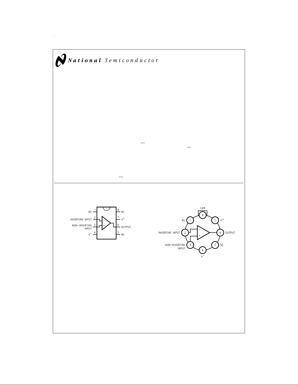
Connection Diagrams
8-Pin DIP
Top View
8-Pin Metal Can
DS011887-1
DS011887-2
Top View
© 1999 National Semiconductor Corporation DS011887 www.national.com
Page 2
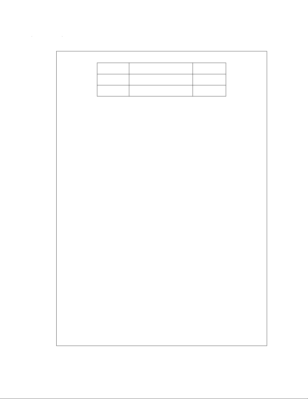
Ordering Information
Package Industrial Temperature Range NSC Package
8-Pin LMC6001AIN, LMC6001BIN, N08E
Molded DIP LMC6001CIN
8-Pin LMC6001AIH, LMC6001BIH H08C
Metal Can
−40˚C to +85˚C Drawing
www.national.com 2
Page 3
Absolute Maximum Ratings (Note 1)
If Military/Aerospace specified devices are required,
please contact the National Semiconductor Sales Office/
Distributors for availability and specifications.
Differential Input Voltage
Voltage at Input/Output Pin (V
Supply Voltage (V
Output Short Circuit to V
Output Short Circuit to V
+−V−
) −0.3V to +16V
+
−
Lead Temperature
(Soldering, 10 Sec.) 260˚C
Storage Temperature −65˚C to +150˚C
Junction Temperature 150˚C
Current at Input Pin
Current at Output Pin
±
Supply Voltage
+
) + 0.3V, (V−) − 0.3V
(Notes 2, 10)
(Note 2)
±
10 mA
±
30 mA
Current at Power Supply Pin 40 mA
Power Dissipation (Note 9)
ESD Tolerance (Note 9) 2 kV
Operating Ratings (Note 1)
Temperature Range
LMC6001AI, LMC6001BI, LMC6001CI
−40˚C ≤ T
Supply Voltage 4.5V ≤ V
Thermal Resistance (Note 11)
θ
JA
θ
JA
θ
JC
Power Dissipation (Note 8)
≤ +85˚C
J
+
≤ 15.5V
, N Package 100˚C/W
, H Package 145˚C/W
, H Package 45˚C/W
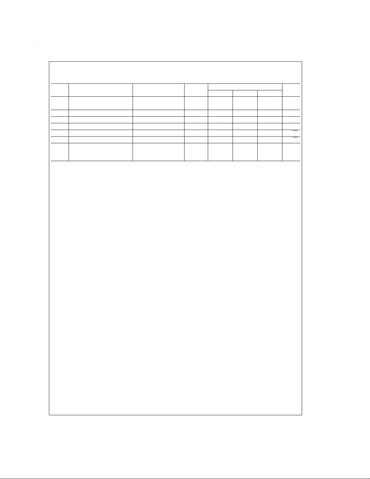
DC Electrical Characteristics
Limits in standard typeface guaranteed for T
otherwise specified, V
+
=
5V, V
−
=
0V, V
Symbol Parameter Conditions
I
B
I
OS
V
OS
TCV
Input Current Either Input, V
Input Offset Current 5 1000 2000 2000
Input Offset Voltage 0.35 1.0 1.0
Input Offset 2.5 10 10 µV/˚C
OS
Voltage Drift
R
IN
Input Resistance
CMRR Common Mode 0V ≤ V
Rejection Ratio V
+PSRR Positive Power Supply 5V ≤ V
Rejection Ratio 70 63 63
−PSRR Negative Power 0V ≥ V
Supply Rejection Ratio 77 71 71
A
V
Large Signal Sourcing, R
Voltage Gain (Note 6) 300 200 200
V
CM
Input Common-Mode V
Voltage For CMRR ≥ 60 dB 000max
V
O
Output Swing V
=
25˚C and limits in boldface type apply at the temperature extremes. Unless
J
=
1.5V, and R
CM
=
S
=
V
S
+
=
Sinking, R
CM
±
5V 2000 4000 4000
±
5V, V
CM
≤ 7.5V 83 75 72 66
CM
10V 72 68 63
+
≤ 15V 83 73 66 66
−
≥ −10V 94 80 74 74
=
2kΩ 1400 400 300 300
L
=
2kΩ 350 180 90 90
L
(Note 6) 100 60 60
+
=
5V and 15V −0.4 −0.1 −0.1 −0.1 V
+
=
5V 4.87 4.80 4.75 4.75 V
=
R
2kΩto 2.5V 4.73 4.67 4.67 min
L
+
=
V
15V 14.63 14.50 14.37 14.37 V
=
R
2kΩto 7.5V 14.34 14.25 14.25 min
L
>
1M.
L
Typical
(Note 4)
=
0V, 10 25 100 1000
LMC6001AI LMC6001BI LMC6001CI
Limits (Note 5) Units
1.0 1.7 2.0
=
0V 0.7 1.35 1.35
1.35 2.0
>
1 Tera Ω
+
V
− 1.9 V+− 2.3 V+− 2.3 V+− 2.3 V
+
V
− 2.5 V+− 2.5 V+− 2.5 min
0.10 0.14 0.20 0.20 V
0.17 0.24 0.24 max
0.26 0.35 0.44 0.44 V
0.45 0.56 0.56 max
fAV
mV
dB
min
V/mV
min
www.national.com3
Page 4
DC Electrical Characteristics (Continued)
Limits in standard typeface guaranteed for T
otherwise specified, V
+
=
5V, V
−
=
0V, V
Symbol Parameter Conditions
I
O
I
S
Output Current Sourcing, V
Supply Current V
=
25˚C and limits in boldface type apply at the temperature extremes. Unless
J
=
1.5V, and R
CM
+
=
5V, 22 16 13 13
=
V
0V 10 8 8
O
+
Sinking, V
V
O
Sourcing, V
V
O
Sinking, V
V
O
+
+
V
=
5V, 21 16 13 13
=
5V 13 10 10
+
=
15V, 30 28 23 23
=
0V 22 18 18
+
=
=
=
=
15V,
13V (Note 10)
=
5V, V
15V, V
1.5V 450 750 750 750
O
=
7.5V 550 850 850 850
O
>
1M.
L
Typical
(Note 4)
LMC6001AI LMC6001BI LMC6001CI
Limits (Note 5) Units
mA
min
34 28 23 23
22 18 18
900 900 900
µA
max
950 950 950
www.national.com 4
Page 5
AC Electrical Characteristics
Limits in standard typeface guaranteed for T
otherwise specified, V
+
=
5V, V
−
=
0V, V
Symbol Parameter Conditions Typical Limits (Note 5) Units
SR Slew Rate (Note 7) 1.5 0.8 0.8 0.8 V/µs
GBW Gain-Bandwidth Product 1.3 MHz
φf
G
e
i
n
Phase Margin 50 Deg
m
Gain Margin 17 dB
M
Input-Referred Voltage Noise F=1 kHz 22 nV/√Hz
n
Input-Referred Current Noise F=1 kHz 0.13 fA/√Hz
THD Total Harmonic Distortion F=10 kHz, A
Note 1: Absolute Maximum Ratings indicate limits beyond which damage to the device may occur. Operating Ratings indicate conditions for which the device is intended to be functional but do not guarantee specific performance limits. For guaranteed specifications and test conditions, see the Electrical Characteristics. The
guaranteed specifications apply only for the test conditions listed.
Note 2: Applies to both single supply and split supply operation. Continuous short circuit operation at elevated ambient temperature can result in exceeding the maximum allowed junction temperature of 150˚C. Output currents in excess of
Note 3: The maximum power dissipation is a function of T
=
P
(T
D
Note 4: Typical values represent the most likely parametric norm.
Note 5: All limits are guaranteed by testing or statistical analysis.
Note 6: V
Note 7: V
Note 8: For operating at elevated temperatures the device must be derated based on the thermal resistance θ
Note 9: Human body model, 1.5 kΩ in series with 100 pF.
Note 10: Do not connect the output to V
Note 11: All numbers apply for packages soldered directly into a printed circuit board.
)/θJA.
J(max)−TA
+
=
+
=
=
15V, V
15V. Connected as Voltage Follower with 10V step input. Limit specified is the lower of the positive and negative slew rates.
CM
7.5V and R
connected to 7.5V. For Sourcing tests, 7.5V ≤ VO≤ 11.5V. For Sinking tests, 2.5V ≤ VO≤ 7.5V.
L
+
, when V+is greater than 13V or reliability will be adversely affected.
=
25˚C and limits in boldface type apply at the temperature extremes. Unless
J
CM
=
1.5V and R
>
1M.
L
(Note 4) LM6001AI LM6001BI LM6001CI
0.6 0.6 0.6 min
=
−10,
=
R
L
=
V
O
V
100 kΩ,
8V
PP
±
30 mA over long term may adversely affect reliability.
, θJA, and TA. The maximum allowable power dissipation at any ambient temperature is
J(max)
0.01
JA
with P
=
)/θJA.
(T
D
J−TA
%
www.national.com5
Page 6

Typical Performance Characteristics V
Input Current
vs Temperature
Input Current
vs V
CMVS
=
±
5V
=
±
S
7.5V, T
=
25˚C, unless otherwise specified
A
Supply Current
vs Supply Voltage
Input Voltage
vs Output Voltage
Input Voltage Noise
vs Frequency
DS011887-16
DS011887-19
DS011887-22
Common Mode Rejection
Ratio vs Frequency
Noise Figure
vs Source Resistance
DS011887-17
DS011887-20
DS011887-23
DS011887-18
Power Supply Rejection
Ratio vs Frequency
DS011887-21
Output Characteristics
Sourcing Current
DS011887-24
www.national.com 6
Page 7

Typical Performance Characteristics V
specified (Continued)
=
±
7.5V, T
S
=
25˚C, unless otherwise
A
Output Characteristics
Sinking Current
Open Loop
Frequency Response
DS011887-25
DS011887-28
Gain and Phase Response
vs Temperature
(−55˚C to +125˚C)
Inverting Small Signal
Pulse Response
DS011887-26
DS011887-29
Gain and Phase
Response vs Capacitive Load
=
with R
L
500 kΩ
Inverting Large Signal
Pulse Response
DS011887-30
DS011887-27
Non-Inverting Small
Signal Pulse Response
DS011887-31
Non-Inverting Large
Signal Pulse Response
Applications Hints
AMPLIFIER TOPOLOGY
The LMC6001 incorporates a novel op-amp design topology
that enables it to maintain rail-to-rail output swing even when
driving a large load. Instead of relying on a push-pull unity
gain output buffer stage, the output stage is taken directly
from the internal integrator, which provides both low output
impedance and large gain. Special feed-forward compensation design techniques are incorporated to maintain stability
over a wider range of operating conditions than traditional
Stability vs
Capacitive Load
DS011887-32
DS011887-33
op-amps. These features make the LMC6001 both easier to
design with, and provide higher speed than products typically found in this low power class.
COMPENSATING FOR INPUT CAPACITANCE
It is quite common to use large values of feedback resistance for amplifiers with ultra-low input current, like the
LMC6001.
www.national.com7
Page 8

Applications Hints (Continued)
Although the LMC6001 is highly stable over a wide range of
operating conditions, certain precautions must be met to
achieve the desired pulse response when a large feedback
resistor is used. Large feedback resistors with even small
values of input capacitance, due to transducers, photodiodes, and circuit board parasitics, reduce phase margins.
When high input impedances are demanded, guarding of the
LMC6001 is suggested. Guarding input lines will not only reduce leakage, but lowers stray input capacitance as well.
(See
Printed-Circuit-Board Layout for High Impedance
Work
).
The effect of input capacitance can be compensated for by
adding a capacitor, C
Figure 1
) such that:
Since it is often difficult to know the exact value of CIN,Cfcan
be experimentally adjusted so that the desired pulse response is achieved. Refer to the LMC660 and LMC662 for a
more detailed discussion on compensating for input
capacitance.
, around the feedback resistors (as in
f
or
≤ R2C
R
1CIN
f
DS011887-6
FIGURE 2. LMC6001 Noninverting Gain of 10 Amplifier,
Compensated to Handle Capacitive Loads
In the circuit of
Figure 2
, R1 and C1 serve to counteract the
loss of phase margin by feeding the high frequency component of the output signal back to the amplifier’s inverting input, thereby preserving phase margin in the overall feedback
loop.
Capacitive load driving capability is enhanced by using a pullup resistor to V
+
(
Figure 3
). Typically a pullup resistor conducting 500 µA or more will significantly improve capacitive
load responses. The value of the pullup resistor must be determined based on the current sinking capability of the amplifier with respect to the desired output swing. Open loop gain
of the amplifier can also be affected by the pullup resistor
(see Electrical Characteristics).
DS011887-5
FIGURE 1. Cancelling the Effect of Input Capacitance
CAPACITIVE LOAD TOLERANCE
All rail-to-rail output swing operational amplifiers have voltage gain in the output stage. A compensation capacitor is
normally included in this integrator stage. The frequency location of the dominant pole is affected by the resistive load
on the amplifier.Capacitive load driving capability can be optimized by using an appropriate resistive load in parallel with
the capacitive load (see Typical Curves).
Direct capacitive loading will reduce the phase margin of
many op-amps. A pole in the feedback loop is created by the
combination of the op-amp’s output impedance and the capacitive load. This pole induces phase lag at the unity-gain
crossover frequency of the amplifier resulting in either an oscillatory or underdamped pulse response. With a few external components, op amps can easily indirectly drive capacitive loads, as shown in
www.national.com 8
Figure 2
.
DS011887-7
FIGURE 3. Compensating for Large Capacitive
Loads with a Pullup Resistor
PRINTED-CIRCUIT-BOARD LAYOUT
FOR HIGH-IMPEDANCE WORK
It is generally recognized that any circuit which must operate
with less than 1000 pA of leakage current requires special
layout of the PC board. When one wishes to take advantage
of the ultra-low bias current of the LMC6001, typically less
than 10 fA, it is essential to have an excellent layout. Fortunately, the techniques of obtaining low leakages are quite
simple. First, the user must not ignore the surface leakage of
the PC board, even though it may sometimes appear acceptably low, because under conditions of high humidity or dust
or contamination, the surface leakage will be appreciable.
To minimize the effect of any surface leakage, lay out a ring
of foil completely surrounding the LMC6001’s inputs and the
terminals of capacitors, diodes, conductors, resistors, relay
terminals, etc., connected to the op-amp’s inputs, as in
Fig-
Page 9

Applications Hints (Continued)
ure 4
. To have a significant effect, guard rings should be
placed on both the top and bottom of the PC board. This PC
foil must then be connected to a voltage which is at the same
voltage as the amplifier inputs, since no leakage current can
flow between two points at the same potential. For example,
a PC board trace-to-pad resistance of 10
mally considered a very large resistance, could leak 5 pA if
the trace were a 5V bus adjacent to the pad of the input.
This would cause a 500 times degradation from the
LMC6001’s actual performance. If a guard ring is used and
held within 1 mV of the inputs, then the same resistance of
12
10
Ω will only cause 10 fA of leakage current. Even this
small amount of leakage will degrade the extremely low input
current performance of the LMC6001. See
cal connections of guard rings for standard op-amp
configurations.
12
Ω, which is nor-
Figure 5
for typi-
The designer should be aware that when it is inappropriate
to lay out a PC board for the sake of just a few circuits, there
is another technique which is even better than a guard ring
on a PC board: Don’t insert the amplifier’s input pin into the
board at all, but bend it up in the air and use only air as an insulator. Air is an excellent insulator. In this case you may
have to forego some of the advantages of PC board construction, but the advantages are sometimes well worth the
effort of using point-to-point up-in-the-air wiring. See
6
.
Figure
FIGURE 4. Examples of Guard
Ring in PC Board Layout
DS011887-9
Inverting Amplifier
DS011887-8
(Input pins are lifted out of PC board and soldered directly to components.
All other pins connected to PC board).
DS011887-12
FIGURE 6. Air Wiring
Another potential source of leakage that might be overlooked is the device package. When the LMC6001 is manufactured, the device is always handled with conductive finger
cots. This is to assure that salts and skin oils do not cause
leakage paths on the surface of the package. We recommend that these same precautions be adhered to, during all
phases of inspection, test and assembly.
Latchup
CMOS devices tend to be susceptible to latchup due to their
internal parasitic SCR effects. The (I/O) input and output pins
look similar to the gate of the SCR. There is a minimum current required to trigger the SCR gate lead. The LMC6001 is
designed to withstand 100 mA surge current on the I/O pins.
Some resistive method should be used to isolate any capacitance from supplying excess current to the I/O pins. In addition, like an SCR, there is a minimum holding current for any
latchup mode. Limiting current to the supply pins will also inhibit latchup susceptibility.
Typical Applications
The extremely high input resistance, and low power consumption, of the LMC6001 make it ideal for applications that
require battery-powered instrumentation amplifiers. Examples of these types of applications are hand-held pH
probes, analytic medical instruments, electrostatic field detectors and gas chromotographs.
DS011887-10
Non-Inverting Amplifier
DS011887-11
Follower
FIGURE 5. Typical Connections of Guard Rings
Two Opamp, Temperature
Compensated pH Probe Amplifier
The signal from a pH probe has a typical resistance between
10 MΩ and 1000 MΩ. Because of this high value, it is very
important that the amplifier input currents be as small as
possible. The LMC6001 with less than 25 fA input current is
an ideal choice for this application.
The theoretical output of the standard Ag/AgCl pH probe is
59.16 mV/pH at 25˚C with 0V out at a pH of 7.00. This output
is proportional to absolute temperature. To compensate for
this, a temperature compensating resistor, R1, is placed in
www.national.com9
Page 10

Two Opamp, Temperature
Compensated pH Probe Amplifier
(Continued)
the feedback loop. This cancels the temperature dependence of the probe. This resistor must be mounted where it
will be at the same temperature as the liquid being measured.
The LMC6001 amplifies the probe output providing a scaled
voltage of
a micropower LMC6041 provides phase inversion and offset
so that the output is directly proportional to pH, over the full
range of the probe. The pH reading can now be directly displayed on a low cost, low power digital panel meter. Total
current consumption will be about 1 mA for the whole system.
The micropower dual operational amplifier, LMC6042, would
optimize power consumption but not offer these advantages:
±
100 mV/pH from a pH of 7. The second opamp,
1. The LMC6001A guarantees a 25 fA limit on input current
at 25˚C.
2. The input ESD protection diodes in the LMC6042 are
only rated at 500V while the LMC6001 has much more
robust protection that is rated at 2000V.
The setup and calibration is simple with no interactions to
cause problems.
1. Disconnect the pH probe and with R3 set to about
mid-range and the noninverting input of the LMC6001
grounded, adjust R8 until the output is 700 mV.
2. Apply −414.1 mV to the noninverting input of the
LMC6001. Adjust R3 for and output of 1400 mV. This
completes the calibration. As real pH probes may not
perform exactly to theory, minor gain and offset adjustments should be made by trimming while measuring a
precision buffer solution.
R1 100k + 3500 ppm/˚C (Note 12)
R2 68.1k
R3,85k
R4, 9 100k
R5 36.5k
R6 619k
R7 97.6k
D1 LM4040D1Z-2.5
C1 2.2 µF
Note 12: (Micro-ohm style 144 or similar)
FIGURE 7. pH Probe Amplifier
Ultra-Low Input Current Instrumentation Amplifier
Figure 8
high differential and common mode input resistance
(
CMRR with 1 MΩ imbalance in source resistance. Input cur-
shows an instrumentation amplifier that features
>
1014Ω), 0.01%gain accuracy at A
V
=
1000, excellent
rent is less than 20 fA and offset drift is less than 2.5 µV/˚C.
www.national.com 10
R
provides a simple means of adjusting gain over a wide
2
range without degrading CMRR. R
maximize CMRR without using super precision matched resistors. For good CMRR over temperature, low drift resistors
should be used.
DS011887-15
is an initial trim used to
7
Page 11

Ultra-Low Input Current Instrumentation Amplifier (Continued)
=
If R
∴
AV≈ 100 for circuit shown (R
=
, and R
R
5,R3
R
6
1
=
; then
R
4
7
=
9.85k).
2
DS011887-13
FIGURE 8. Instrumentation Amplifier
www.national.com11
Page 12

12
Page 13

Physical Dimensions inches (millimeters) unless otherwise noted
8-Pin Metal Can Package (H)
Order Number LMC6001AIH or LMC6001BIH
NS Package Number H08C
Order Number LMC6001AIN, LMC6001BIN or LMC6001CIN
8-Pin Molded Dual-In-Line Package
NS Package Number N08E
www.national.com13
Page 14

Physical Dimensions inches (millimeters) unless otherwise noted (Continued)
LMC6001 Ultra Ultra-Low Input Current Amplifier
LIFE SUPPORT POLICY
NATIONAL’S PRODUCTS ARE NOT AUTHORIZED FOR USE AS CRITICAL COMPONENTS IN LIFE SUPPORT DEVICES OR SYSTEMS WITHOUT THE EXPRESS WRITTEN APPROVAL OF THE PRESIDENT OF NATIONAL SEMICONDUCTOR CORPORATION. As used herein:
1. Life support devices or systems are devices or systems which, (a) are intended for surgical implant into
the body, or (b) support or sustain life, and whose failure to perform when properly used in accordance
2. A critical component is any component of a life support
device or system whose failure to perform can be reasonably expected to cause the failure of the life support
device or system, or to affect its safety or effectiveness.
with instructions for use provided in the labeling, can
be reasonably expected to result in a significant injury
to the user.
National Semiconductor
Corporation
Americas
Tel: 1-800-272-9959
Fax: 1-800-737-7018
Email: support@nsc.com
www.national.com
National does not assume any responsibility for use of any circuitry described, no circuit patent licenses are implied and National reserves the right at any time without notice to change said circuitry and specifications.
National Semiconductor
Europe
Fax: +49 (0) 1 80-530 85 86
Email: europe.support@nsc.com
Deutsch Tel: +49 (0) 1 80-530 85 85
English Tel: +49 (0) 1 80-532 78 32
Français Tel: +49 (0) 1 80-532 93 58
Italiano Tel: +49 (0) 1 80-534 16 80
National Semiconductor
Asia Pacific Customer
Response Group
Tel: 65-2544466
Fax: 65-2504466
Email: sea.support@nsc.com
National Semiconductor
Japan Ltd.
Tel: 81-3-5639-7560
Fax: 81-3-5639-7507
 Loading...