

Page 1
LMC568
Low Power Phase-Locked Loop
General Description
The LMC568 is an amplitude-linear phase-locked loop consisting of a linear VCO, fully balanced phase detectors, and
a carrier detect output. LMCMOS
™
technology is employed
for high performance with low power consumption.
The VCO has a linearized control range of
±
30%to allow demodulation of FM and FSK signals. Carrier detect is indicated when the PLL is locked to an input signal greater than
26 mVrms. LMC568 applications include FM SCA and TV
second audio program decoders, FSK data demodulators,
and voice pagers.
Features
n Demodulates±15%deviation FM/FSK signals
n Carrier Detect Output with hysteresis
n Operation to 500 kHz input frequency
n Low THD—0.5%typ. for
±
10%deviation
n 2V to 9V supply voltage range
n Low supply current drain
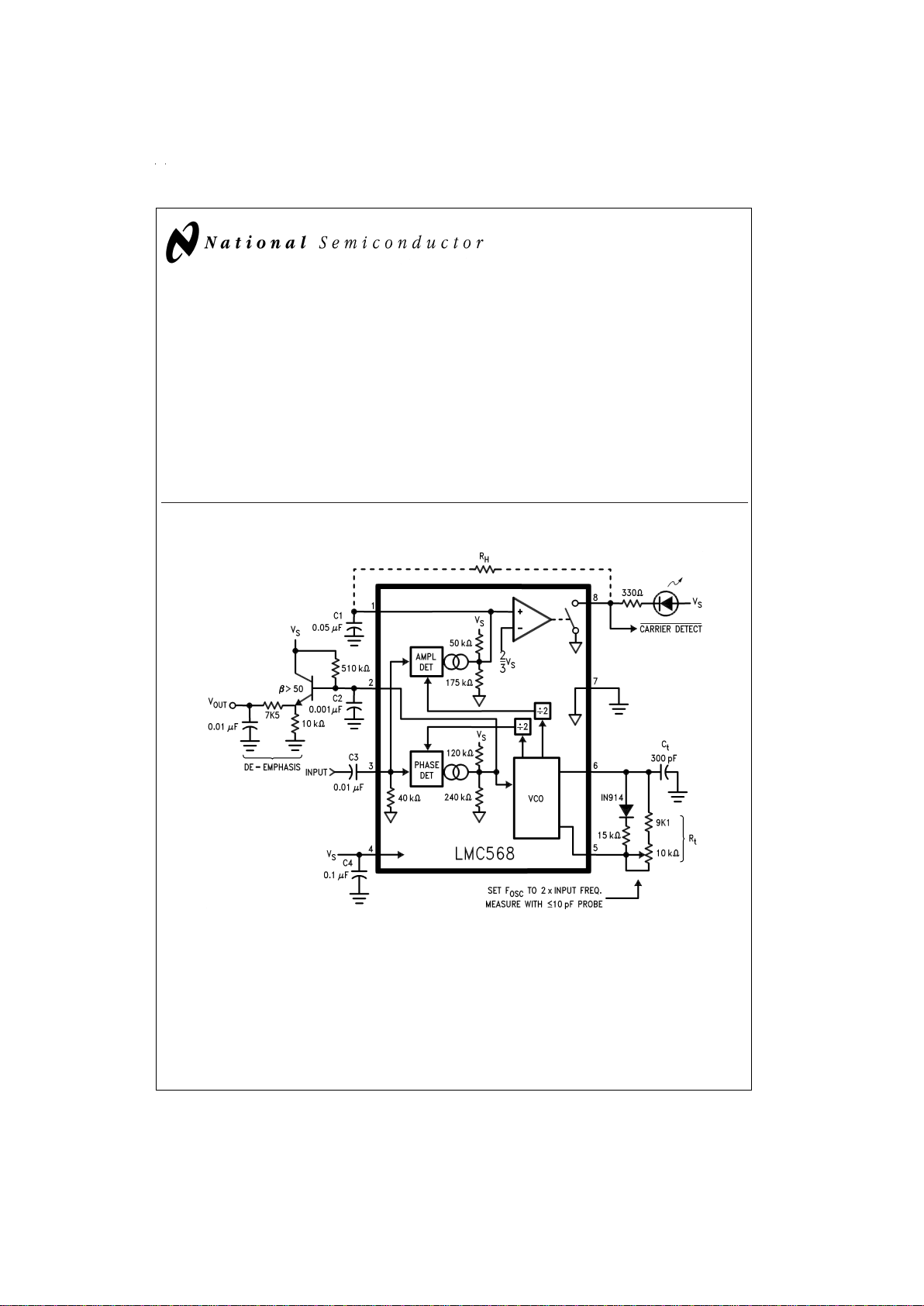
Typical Application (100 kHz input frequency, refer to notes pg. 3)
LMCMOS™is a trademark of NationalSemiconductor Corporation.
DS009135-1
Order Number LMC568CM or LMC568CN
See NS Package Number M08A or N08E
May 1999
LMC568 Low Power Phase-Locked Loop
© 1999 National Semiconductor Corporation DS009135 www.national.com
Page 2
Absolute Maximum Ratings (Note 1)
If Military/Aerospace specified devices are required,
please contact the National Semiconductor Sales Office/
Distributors for availability and specifications.
Input Voltage, Pin 3 2 V
p–p
Supply Voltage, Pin 4 10V
Output Voltage, Pin 8 13V
Voltage at All Other Pins V
s
to Gnd
Output Current, Pin 8 30 mA
Package Dissipation 500 mW
Operating Temperature Range (T
A
) −25˚C to +125˚C
Storage Temperature Range −55˚C to +150˚C
Soldering Information
Dual-In-Line Package
Soldering (10 seconds) 260˚C
Small Outline Package
Vapor Phase (60 seconds) 215˚C
Infrared (15 seconds) 220˚C
See AN-450 “Surface Mounting Methods and their Effect
on Product Reliability” for other methods of soldering
surface mount devices.
Note 1: “Absolute Maximum Ratings” indicate limits beyond which damage
to the device may occur. Operating Ratings indicate conditions for which the
device is functional, but do not guarantee specific performance limits.
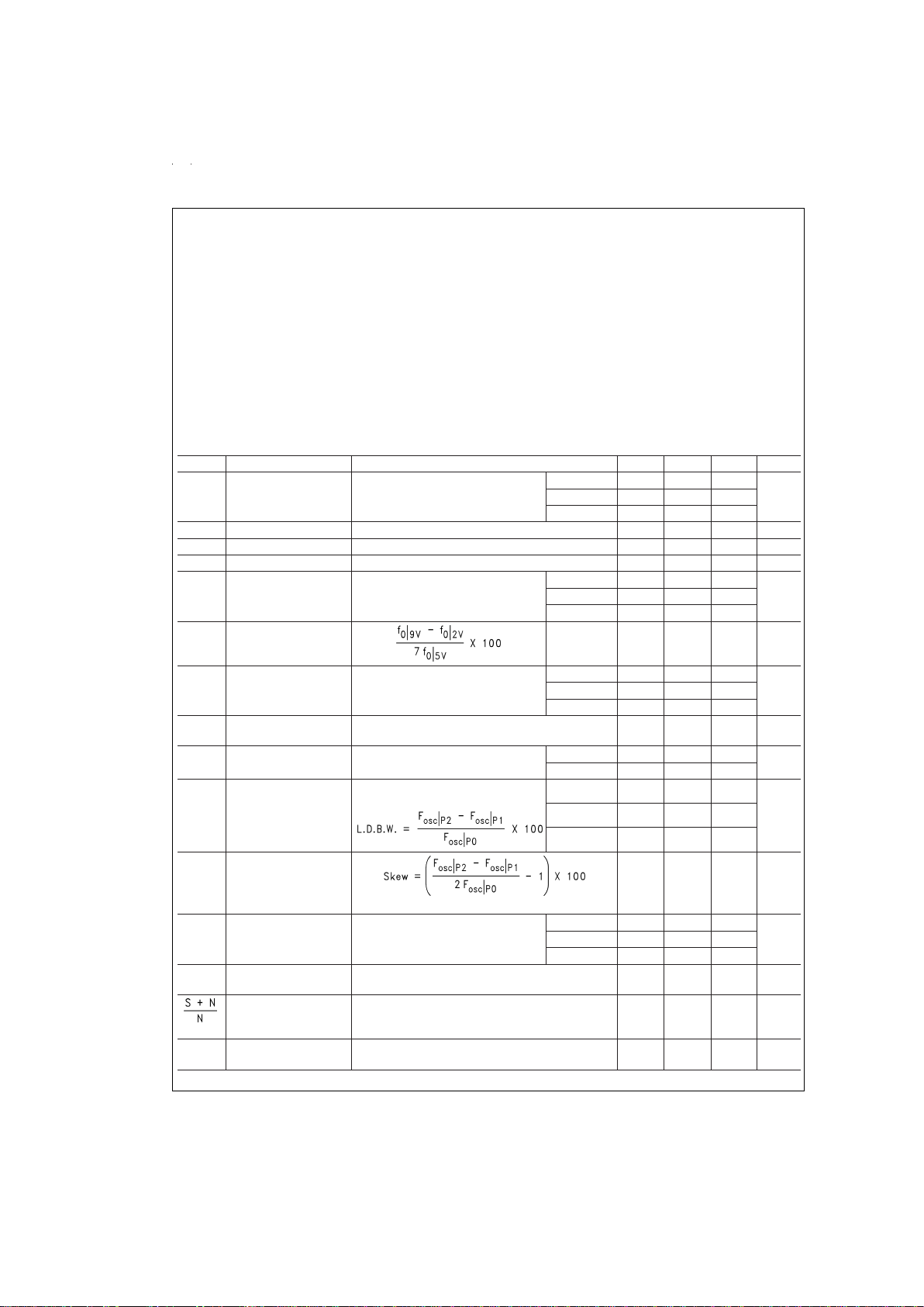
Electrical Characteristics
Test Circuit, T
A
=
25˚C, V
S
=
5V, RtCt
#
2, Sw. 1 Pos. 0; and no input unless otherwise noted.
Symbol Parameter Conditions Min Typ Max Units
I4 Power Supply Current RtCt
#
1, Quiescent or Activated VS= 2V 0.35
mAdcV
S
= 5V 0.75 1.5
V
S
= 9V 1.2 2.4
V3 Input D.C. Bias 0 mVdc
R3 Input Resistance 40 kΩ
I8 Output Leakage 1 100 nAdc
f
0
Center Frequency F
osc
÷
2
RtCt #2, Measure Oscillator
Frequency and Divide by 2
V
S
=2V 98
kHzV
S
= 5V 90 103 115
V
S
= 9V 105
∆f
0
Center Frequency Shift
with Supply
1.0 2.0
%
/V
V
in
Input Threshold Set Input Frequency Equal to f
0
Measured Above, Increase Input
Level until Pin 8 Goes Low.
V
S
= 2V 8 16 25
mVrmsV
S
=5V 15 26 42
V
S
=9V 45
∆V
in
Input Hysteresis Starting at Input Threshold, Decrease Input Level
until Pin 8 Goes High
1.5 mVrms
V8 Output ″Sat″ Voltage Input Level
>
Threshold Choose RL
for Specified I8
I8=2mA 0.06 0.15
Vdc
I8=20mA 0.7
L.D.B.W. Largest Detection
Bandwidth
Measure F
osc
with Sw. 1 in Pos. 0, 1,
and 2;
VS=2V
30
%
V
S
=5V
40 55
V
S
=9V
60
∆BW Bandwidth Skew
1
±
5
%
V
out
Recovered Audio Typical Application Circuit
Input = 100 mVrms, F = 100 kHz
F
mod
= 400 Hz,±10 kHz Dev.
V
S
= 2V 170
mVrmsV
S
= 5V 270
V
S
= 9V 400
THD Total Harmonic
Distortion
Typical Application Circuit as Above, Measure V
out
Distortion.
0.5
%
Signal to Noise Ratio Typical Application Circuit
Remove Modulation, Measure V
n
(S + N)/N = 20 log (V
out/Vn
).
65 dB
f
max
Highest Center Freq. RtCt #3, Measure Oscillator Frequency and Divide by
2
700 kHz
www.national.com 2
Page 3
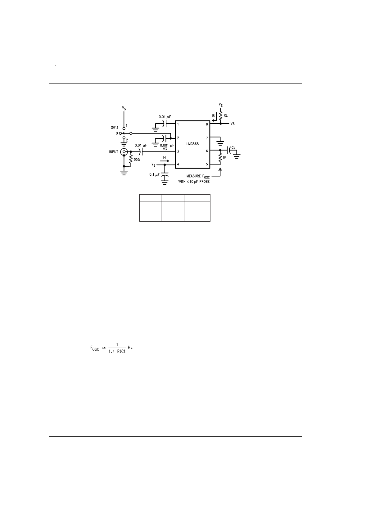
Test Circuit
RtCt Rt Ct
#
1 100k 300 pF
#
2 10k 300 pF
#
3 5.1k 62 pF
Notes to Typical Application
SUPPLY DECOUPLING
The decoupling of supply pin 4 becomes more critical at high
supply voltages with high operating frequencies, requiring
C4 to be placed as close to possible to pin 4. Also, due to pin
voltages tracking supply, a large C4 is necessary for low frequency PSRR.
OSCILLATOR TIMING COMPONENTS
The voltage-controlled oscillator (VCO) on the LMC568 must
be set up to run at twice the frequency of the input signal.
The components shown in the typical application are for F
osc
=
200 kHz (100 kHz input frequency). For operation at lower
frequencies, increase the capacitor value; for higher frequencies proportionally reduce the resistor values.
If low distortion is not a requirement, the series diode/resistor
between pins 6 and 5 may be omitted. This will reduce VCO
supply dependence and increase V
out
by approximately 2 dB
with THD=2%typical. The center frequency as a function of
Rt and Ct is given by:
To allow for I.C. and component value tolerences, the oscillator timing components will require a trim. This is generally
accomplished by using a variable resistor as part of Rt, although Ct could also be padded. The amount of initial frequency variation due to the LMC568 itself is given in the
electrical specifications; the total trim range must also accommodate the tolerances of Rt and Ct.
INPUT PIN
The input pin 3 is internally ground-referenced with a nominal 40 kΩ resistor. Signals that are centered on 0V may be
directly coupled to pin 3; however, any d.c. potential must be
isolated via C3.
OUTPUT TAKEOFF
The output signal is taken off the loop filter at pin 2. Pin 2 is
the combined output of the phase detector and control input
of the VCO for the phase-locked loop (PLL). The nominal pin
2 source resistance is 80 kΩ, requiring the use of an external
buffer transistor to drive nominal loads.
For small values of C2, the PLL will have a fast acquisition
time and the pull-in range will be set by the built-in VCO frequency stops, which also determine the largest detection
bandwidth (LDBW). Increasing C2 results in improved noise
immunity at the expense of acquisition time, and the pull-in
range will become narrower than the LDBW. However, the
maximum hold-in range will always equal the LDBW. The 2
kHz de-emphasis pole shown may be modified or omitted as
required by the application.
CARRIER DETECT
Pin 1 is the output of a negative-going amplitude detector
which has a nominal 0 signal output of 7/9 V
s
. The output at
pin 8 is an N-channel FET switch to ground which is activated when the PLL is locked and the input is of sufficient
amplitude to cause pin 1 to fall below 2/3 V
s
. The carrier detect threshold is internally set to 26 mVrms typical on a 5V
supply.
Capacitor C1 in conjunction with the nominal 40 kΩ pin 1 internal resistance forms the output filter. The size of C1 is a
tradeoff between slew rate and carrier ripple at the output
comparator. Optional resistor R
H
increases the hysteresis in
the pin 8 output for applications such as audio mute control.
The minimum allowable value for R
H
is 330 kΩ.
DS009135-3
www.national.com3
Page 4
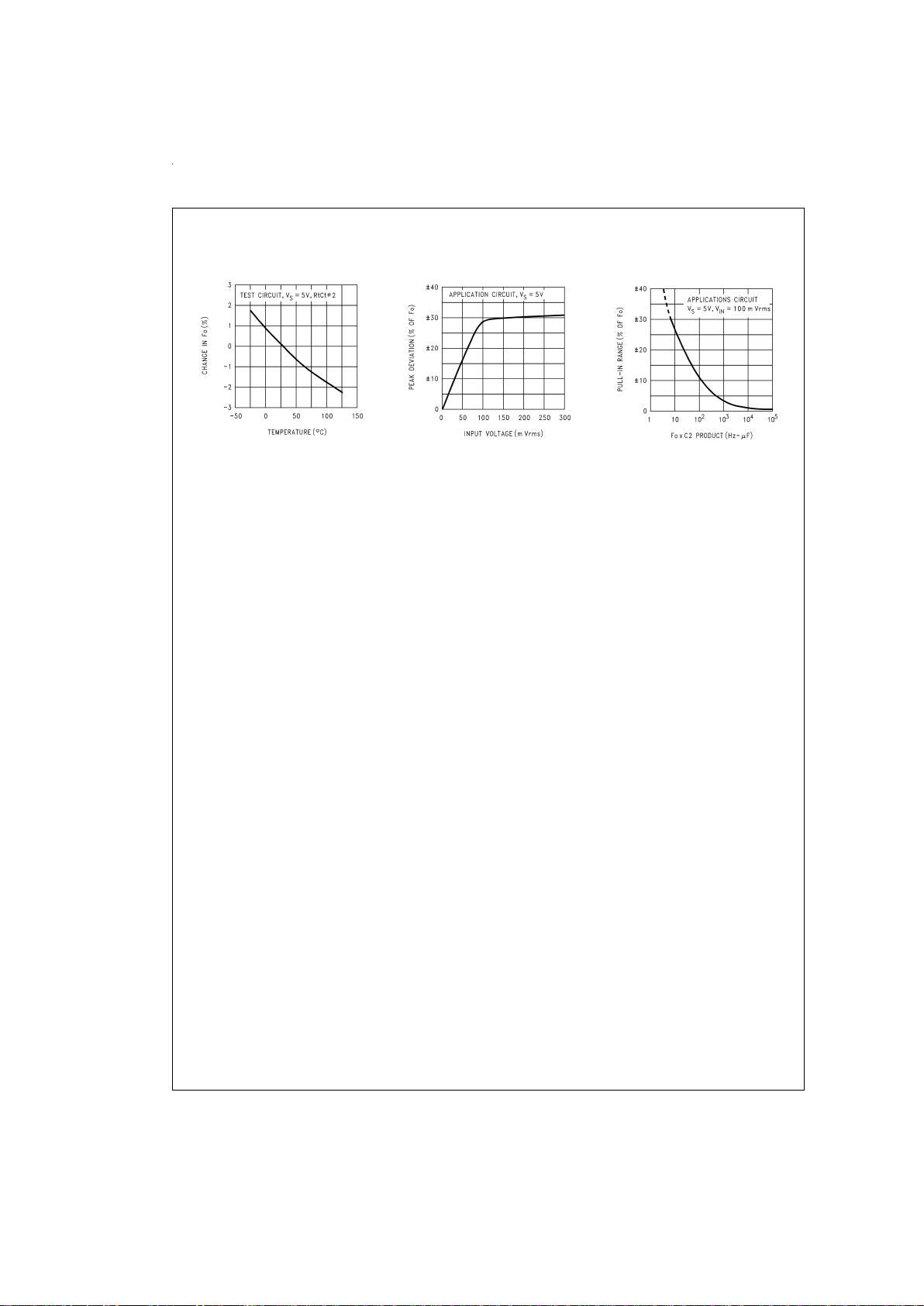
LMC568 Typical Performance Characteristics
Frequency Drift
with Temperature
DS009135-7
Peak Deviation vs
Input Signal Level
DS009135-8
Pull-In Range as
a Function of C2
DS009135-9
www.national.com 4
Page 5
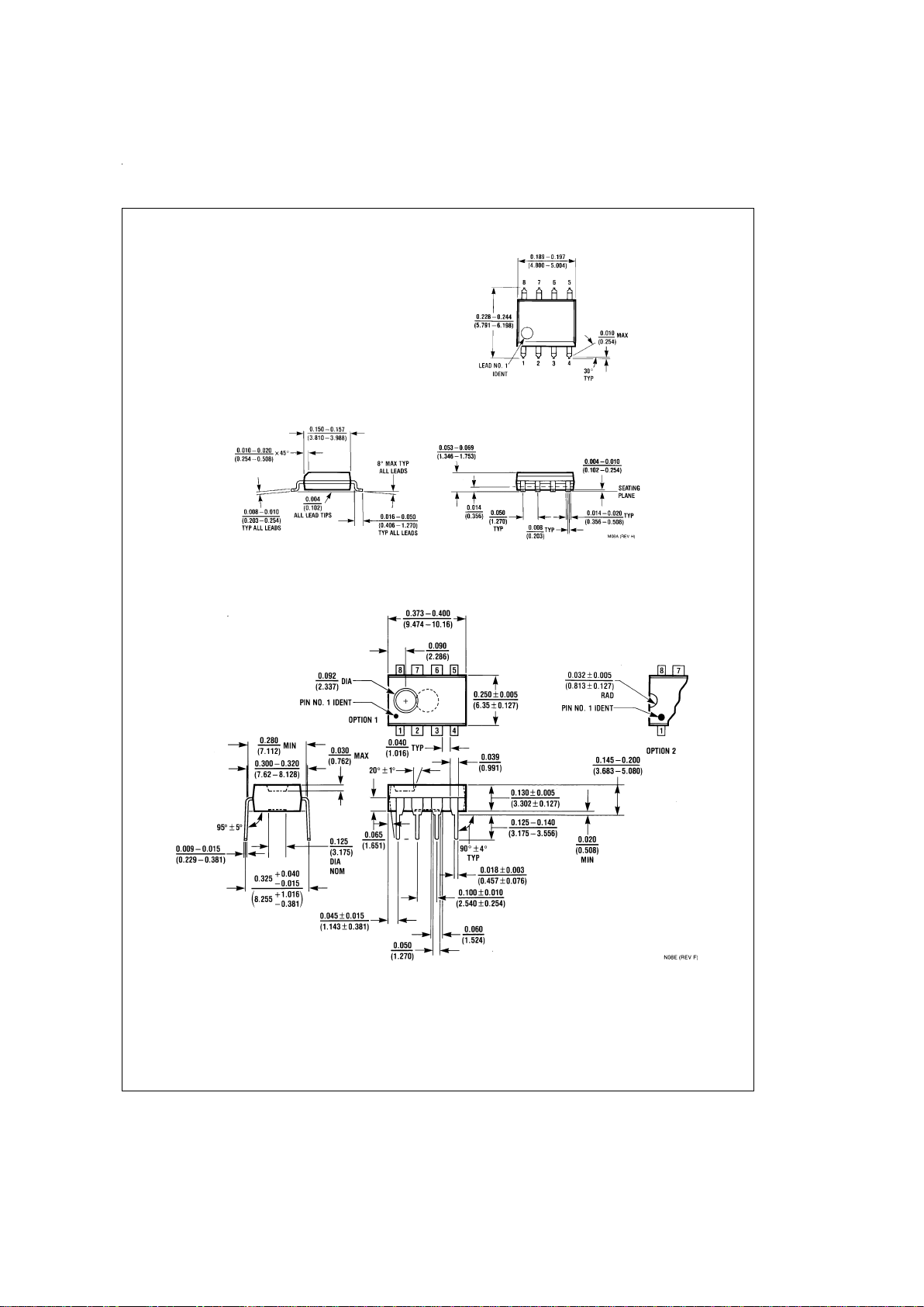
Physical Dimensions inches (millimeters) unless otherwise noted
SO Package (M)
Order Number LMC568CM
NS Package Number M08A
Molded Dual-In-Line Package (N)
Order Number LMC568CN
NS Package Number N08E
www.national.com5
Page 6

Notes
LIFE SUPPORT POLICY
NATIONAL’S PRODUCTS ARE NOT AUTHORIZED FOR USE AS CRITICAL COMPONENTS IN LIFE SUPPORT
DEVICES OR SYSTEMS WITHOUT THE EXPRESS WRITTEN APPROVAL OF THE PRESIDENT AND GENERAL
COUNSEL OF NATIONAL SEMICONDUCTOR CORPORATION. As used herein:
1. Life support devices or systems are devices or
systems which, (a) are intended for surgical implant
into the body, or (b) support or sustain life, and
whose failure to perform when properly used in
accordance with instructions for use provided in the
labeling, can be reasonably expected to result in a
significant injury to the user.
2. A critical component is any component of a life
support device or system whose failure to perform
can be reasonably expected to cause the failure of
the life support device or system, or to affect its
safety or effectiveness.
National Semiconductor
Corporation
Americas
Tel: 1-800-272-9959
Fax: 1-800-737-7018
Email: [email protected]
National Semiconductor
Europe
Fax: +49 (0) 1 80-530 85 86
Email: [email protected]
Deutsch Tel: +49 (0) 1 80-530 85 85
English Tel: +49 (0) 1 80-532 78 32
Français Tel: +49 (0) 1 80-532 93 58
Italiano Tel: +49 (0) 1 80-534 16 80
National Semiconductor
Asia Pacific Customer
Response Group
Tel: 65-2544466
Fax: 65-2504466
Email: [email protected]
National Semiconductor
Japan Ltd.
Tel: 81-3-5639-7560
Fax: 81-3-5639-7507
www.national.com
LMC568 Low Power Phase-Locked Loop
National does not assume any responsibility for use of any circuitry described, no circuit patent licenses are implied and National reserves the right at any time without notice to change said circuitry and specifications.
 Loading...