

Page 1
TL/H/12541
LMC2626 CMOS LDOR/Buffer Chip for Row Inversion Flat Panel Display Systems
PRELIMINARY
November 1995
LMC2626
CMOS LDOR/Buffer Chip for Row
Inversion Flat Panel Display Systems
General Description
The LMC2626 integrated circuit is specifically developed for
a row inversion TFT FPD system architecture. It is designed
only to be used in conjunction with National’s LM2625
switching regulator chip.
Built on National’s advanced CMOS CS80 process, this chip
generates a high-power, precision square-wave from a digital sync signal. The chip also contains thermal shutdown
circuitry, system shutdown circuitry, and a low drop-out voltage regulator to generate a 4.2 volt supply from an externally applied reference voltage of 1.227V.
Features
Y
Used in conjunction with LM2625 chip
Y
High output current buffer
Y
Low buffer on resistance
Y
System shutdown control
Y
LDO voltage regulator
Y
LDOR dropout 0.3V maximum at 150 mA
Y
Thermal shutdown/short circuit protection
Y
External reference required for LDOR
Y
V
REF
pin converts to a digital pin to shutdown LM2625
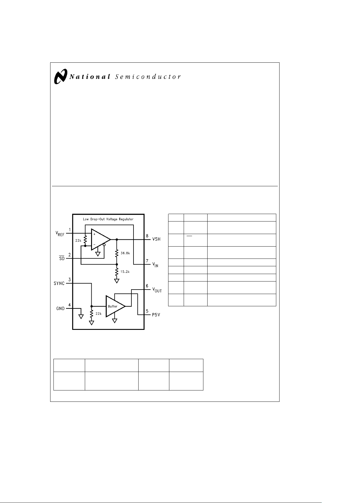
Connection Diagram
8-Pin SO
TL/H/12541– 1
Top View
Pin Description
PinÝPin Name Description
1V
REF
1.218V to 1.242V Ext. Reference
from LM2625 (see Note 8)
2SD System Shutdown input pin for
LMC2626 and LMC2625
3 SYNC Digital input square wave from FPD
controller
4 GND Ground
5 P5V Precision Regulateda5V Supply
6V
OUT
Power Buffer Output
7VINFPD System Supply (a4.5V to
a
5.5V)
8VSHLow Drop-Out Voltage Regulator
Output
Ordering Information
Package
Temperature Range NSC Transport
b
40§Ctoa85§C Drawing Media
8-Pin SO LMC2626IM M08A Rail
Tape and
Reel
C
1996 National Semiconductor Corporation RRD-B30M26/Printed in U. S. A.
Page 2
Absolute Maximum Ratings (Note 1)
ESD Tolerance 2 kV HBM, 200V MM (Note 4)
Sync Input Voltage P5V
Supply Voltage (V
IN
, P5V) 6.3V
Continuous Total Power Dissipation (Note 1)
Lead Temperature (less than 10 sec) 260§C
Storage Temperature Range
b
65§Ctoa150§C
Junction Temperature 150§C
Operating Ratings (Note 1)
V
IN
Supply Voltage 4.5VsV
IN
s
5.5V
P5V Supply Voltage (Note 5) 4.8VsP5Vs5.2V
Junction Temperature Range
b
25§Ctoa125§C
Ambient Temperature Range
b
40§Ctoa85§C
DC Electrical Characteristics
Unless otherwise specified, all limits guaranteed forb20§CsT
A
s
a
85§C, P5Ve5V and 4.5VsV
IN
s
5.5V, V
REF
e
1.227V
SYNC(OPEN), SD
(OPEN)kP5VeV
IN
e
5V
VSH LDO Voltage Regulator (Notes 7, 10, 11)
Symbol Parameter Conditions Min
Typ
Max Units
(Note 9)
V
O(VREF)
V
REF
Voltage Level SDe0V
in Shutdown I
VREF
eb
1 mA 4.00 4.76 V
V
IN
e
5V
I
VREF
DC Current from
b
40.0
b
13.3
b
5 mA
V
REF
Pin
V
SH
Output Voltage on 4.5VsV
IN
s
5.5V
V
SH
Pin (see Note 2) 20 mAsILs150 mA 4.10 4.20 4.30 V
1.218
s
V
REF
s
1.242
DV
SH
Variation of VSHover 4.5VsV
IN
s
5.5V
4 126 mV
Temperature 20 mA
sILs
150 mA
V
DO
LDOR Voltage Dropout ILe150 mA
0.17 0.30 V
(VIN–VSH)
I
S(VIN)
VINSupply Current 230 394 500 mA
Load Regulation of LDO 4.5VsV
IN
s
5.5V
0.002 0.015 %/mA
Voltage Regulation 20 mA
sILs
150 mA
Line Regulation of LDOR 4.5VsV
IN
s
5.5V
0.24 0.95 %/V
20 mA
sILs
150 mA
T
SD
Thermal Shutdown (see Note 8)
160
§
C
Threshold
I
OUT
Output Load Current (see Note 2) 300 mA
Shutdown Control (Note 8)
Symbol Parameter Conditions Min
Typ
Max Units
(Note 9)
I
IL(SD)
Low Level Input Current V
IN
e
5V
b
300
b
217
b
150 mA
for SD
Pin SDe0V
I
IH(SD)
High Level Input Current SDe5V
310 1000 nA
for SD
Pin
I
s(SD)
VINSupply Current
180 285 400 mA
in Shutdown Mode
C
in(SYNC)
Input Capacitance SYNCe5V
20 pF
at SYNC Pin (Note 6) T
A
e
27§C
2
Page 3

DC Electrical Characteristics
Unless otherwise specified, all limits guaranteed forb20§CsT
A
s
a
85§C, P5Ve5V and 4.5VsV
IN
s
5.5V, V
REF
e
1.227V
SYNC(OPEN), SD
(OPEN)kP5VeV
IN
e
5V (Continued)
Buffer
Symbol Parameter Conditions Min
Typ
Max Units
(Note 9)
V
OUT
Peak to Peak Output SYNCe5V
pp
4.997 4.999 V
Voltage Swing or V
OUT
(no load)
V
OL
Low Level Output SYNCe0V
0.2 2 mV
Voltage (No Load)
V
OH
High Level Output SYNCe5V
4.999 V
Voltage (No Load)
D
VOUT
Variation of V
OUT
0.2 1 3 mV
Over Temperature
V
IH
High Level Input
3.5 5 V
SYNC, SD
Voltage
V
IL
Low Level Input
0 1.5 V
SYNC, SD
Voltage
I
IL(SYNC)
Low Level Input SYNCe0V
5.0 42 1000 nA
Current for SYNC
I
IH(SYNC)
High Level Input SYNCe5V
DC
170 215 275 mA
Current for SYNC
I
OUT-AVE
V
OUT
Maximum Average SYNCe5V
PP
100 mA
Load Current from (see Note 2)
R
ON
On Resistance ILe150 mA
0.9 1.5 X
N-Channel T
A
e
27§C
R
ON
On Resistance ILe150 mA
0.7 1.2 X
P-Channel T
A
e
27§C
R
ON
On Resistance ILe150 mA
0.18 0.6 X
Matching T
A
e
27§C
I
s
Supply Current No SYNC
200 355 950 mA
from P5V
3
Page 4

AC Electrical Characteristics
Unless otherwise specified, all limits guaranteed for T
A
e
27§C, V
IN
ee
P5Ve5V. Other conditions are shown in the test
circuit. Conditions that deviate from those shown in the test circuit are listed in the conditions column.
Symbol Parameter Conditions Min
Typ
Max Units
(Note 9)
t
s(OUT)
Settling Time for V
OUT
To 98% p-p V
OUT
,
5.0 ms
V
IN
e
5V (see Note 3)
Note 1: Absolute Maximum Ratings indicate limits beyond which damage to the device may occur. Operating ratings indicate conditions the device is intended
to be functional, but device parameter specifications may not be guaranteed under these conditions. For guaranteed specifications and test conditions, see
the Electrical Characteristics.
Note 2: The typical junction-ambient thermal resistance of the molded plastic SO(M) package is 155
§
C/W. Therefore the maximum current for the buffer and
voltage regulator are limited to the maximum total power dissipation that the package can allow in order to keep the die comfortably below the maximum
operating junction temperature of 125
§
C.
Note 3: The settling time of the Power Buffer is mostly dependent upon the TFT effective series RC load. The measurement of the settling time is taken for the
application when driving an all black display. The number in the datasheet reflects a series RC load (R
e
6.8X and Ce0.22 mF).
Note 4: Human Body Model 100 pF and 1.5 kX. Machine Model 0X.
Note 5: The precision of the P5V supply determines the output voltage swing precision of the buffer for very small loads. The operating range of P5V in this
datasheet assumes a
g
4% error in V
OUT
p-p such that the total error of the signal at the output of the buffer never exceedsg5%.
Note 6: This capacitance is dominated by the ESD protection zeners connected to the SYNC pin.
Note 7: It is important to understand that the load current of the low drop-out voltage regulator must not drop below 2 mA. Otherwise, the internal error
amplifier will not have sufficient drive capability to the large series pass transistor. If load requirements from the FPD system is less than 2 mA, an external preIoad resistor must be connected from V
SH
to ground in order to satisfy the previously mentioned load requirements.
Note 8: The thermal shutdown mode of the voltage regulator and the system shutdown mode are identical. When either of the two functions are enabled, two
results occur. The pass transistor of the voltage regulator is shut off and The V
REF
pin of the LMC2626 is pulled up to the VINsupply to shutdown the LM2625
switching regulator.
Note 9: Typical values represent the most likely parametric norm.
Note 10: The typical closed loop voltage gain of the low drop-out voltage regulator is 3.44(10.7 dB).
Note 11: The minimum load current of the voltage regulator is a specific parameter used to guarantee that the regulated output voltage of the LDO regulator
stays within the limits specified in the datasheet for 1.216V
k
V
REF
k
1.242V. For applications requiring minimum load current less than 20 mA, regulated
output voltage limits of the voltage regulator and V
REF
voltage range must be carefully determined by characterizing the change in regulated output voltage at
the minimum load current needed.
4
Page 5

5
Page 6

LMC2626 CMOS LDOR/Buffer Chip for Row Inversion Flat Panel Display Systems
Physical Dimensions inches (millimeters)
8-Lead (0.150×Wide) Molded Small Outline Package, JEDEC
Order Number LMC2626IM
NS Package M08A
LIFE SUPPORT POLICY
NATIONAL’S PRODUCTS ARE NOT AUTHORIZED FOR USE AS CRITICAL COMPONENTS IN LIFE SUPPORT
DEVICES OR SYSTEMS WITHOUT THE EXPRESS WRITTEN APPROVAL OF THE PRESIDENT OF NATIONAL
SEMICONDUCTOR CORPORATION. As used herein:
1. Life support devices or systems are devices or 2. A critical component is any component of a life
systems which, (a) are intended for surgical implant support device or system whose failure to perform can
into the body, or (b) support or sustain life, and whose be reasonably expected to cause the failure of the life
failure to perform, when properly used in accordance support device or system, or to affect its safety or
with instructions for use provided in the labeling, can effectiveness.
be reasonably expected to result in a significant injury
to the user.
National Semiconductor National Semiconductor National Semiconductor National Semiconductor
Corporation Europe Hong Kong Ltd. Japan Ltd.
1111 West Bardin Road Fax:
a
49 (0) 180-530 85 86 13th Floor, Straight Block, Tel: 81-043-299-2308
Arlington, TX 76017 Email: europe.support@nsc.com Ocean Centre, 5 Canton Rd. Fax: 81-043-299-2408
Tel: 1(800) 272-9959 Deutsch Tel:
a
49 (0) 180-530 85 85 Tsimshatsui, Kowloon
Fax: 1(800) 737-7018 English Tel:
a
49 (0) 180-532 78 32 Hong Kong
Fran3ais Tel:
a
49 (0) 180-532 93 58 Tel: (852) 2737-1600
Italiano Tel:
a
49 (0) 180-534 16 80 Fax: (852) 2736-9960
National does not assume any responsibility for use of any circuitry described, no circuit patent licenses are implied and National reserves the right at any time without notice to change said circuitry and specifications.
 Loading...