

Page 1
查询LMC1992供应商
LMC1992 Digitally-Controlled Stereo Tone and Volume
Circuit with Four-Channel Input-Selector
December 1994
LMC1992 Digitally-Controlled Stereo Tone and
Volume Circuit with Four-Channel Input Selector
General Description
The LMC1992 is a monolithic integrated circuit that provides
four stereo inputs, bass and treble tone controls, and volume, balance, and front-rear fader controls. These functions
are digitally controlled through a three-wire communication
interface. All of the LMC1992s functions are achieved with
only three external capacitors per channel. It is designed for
line level input signals (300 mV
b
2V) and has a maximum
gain of 0 dB.
The internal design is optimized for external capacitors having values of 0.1 mF or less. This allows the use of chip
capacitors for coupling and tone control functions.
Low noise and distortion result from using analog switches
and thin-film silicon-chromium resistor networks in the signal path.
Volume and fader are at minimum and tone controls are flat
when supply voltage is first applied.
Additional tone control can be achieved using the LMC835
stereo 7-band graphic equalizer connected to the
LMC1992’s select-out/select-in external processor loop.
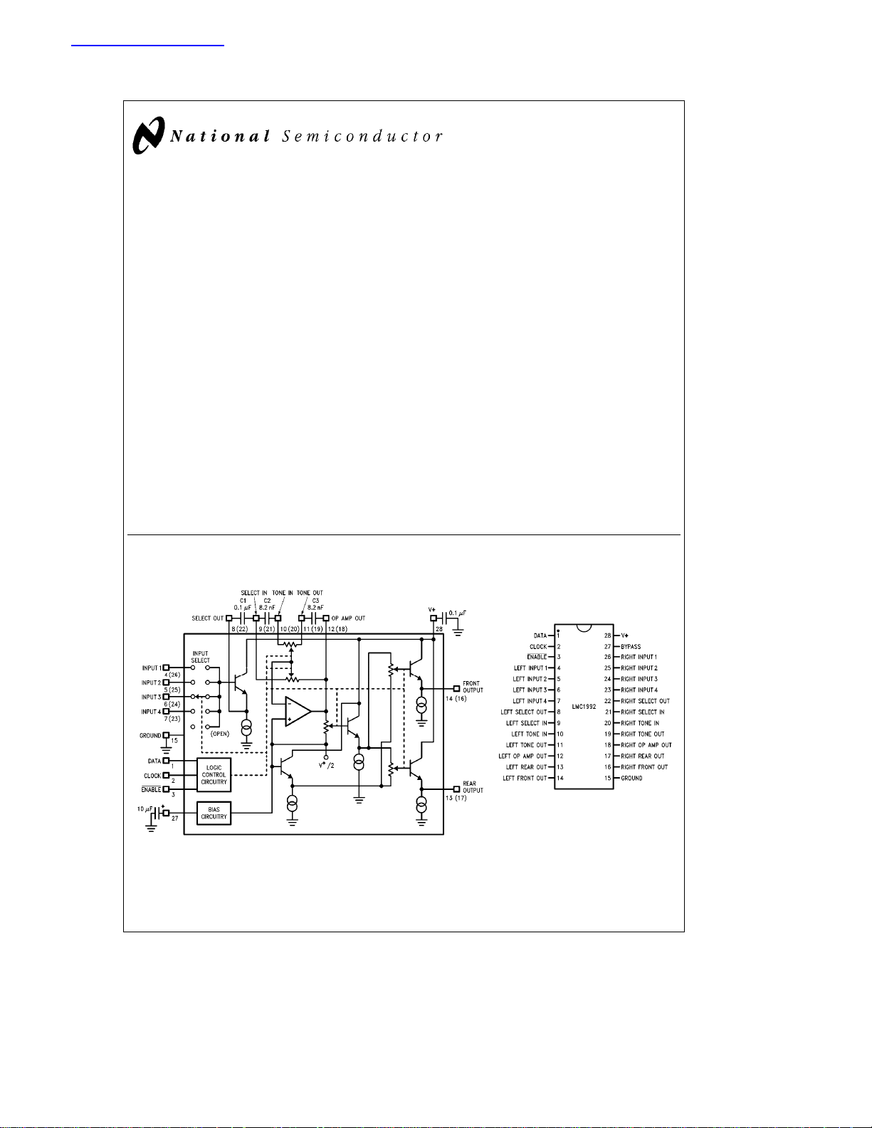
Block and Connection Diagrams
Features
Y
Low noise and distortion
Y
Four stereo inputs
Y
40 volume levels including mute
Y
20 fader levels
Y
All attenuators havea2dBofattenuation per step
Y
Front/back fade control
Y
External processor loop
Y
Only three external components per channel
Y
Serial programmable: standard MICROWIRE
TM
interface
Y
Single supply operation: 6V to 12V supply voltage
Y
Protection address (similar to DS8906)
Y
DC-coupled inputs
Y
Single supply operation
Applications
Y
Automotive audio systems
Y
Sound reinforcement systems
Y
Home entertainmentÐstereo television and music reproduction systems
Y
Electronic music (MIDI)
Order Number LMC1992CCN
TL/H/10789– 2
See NS Package Number N28B
Left channel shown. Pin numbers in parentheses are for the right channel.
DNRÉis a registered trademark of National Semiconductor Corporation.
TM
COPS
and MICROWIRETMare trademarks of National Semiconductor Corporation.
C
1995 National Semiconductor Corporation RRD-B30M75/Printed in U. S. A.
TL/H/10789
TL/H/10789– 1
Page 2
Absolute Maximum Ratings (Notes 1 and 2)
If Military/Aerospace specified devices are required,
please contact the National Semiconductor Sales
Office/Distributors for availability and specifications.
a
Supply Voltage (V
Voltage at Any Pin GNDb0.2V to V
b
GND) 15V
a
a
0.2V
Input Current at Any Pin (Note 3) 5 mA
Package Input Current (Note 3) 20 mA
Power Dissipation (Note 4) 500 mW
Junction Temperature 125
Electrical Characteristics The following specifications apply for V
channel 1, volume
e
0 dB, basse0 dB, treblee0 dB, and faderse0 dB unless otherwise specified. All limits T
§
25§C.
Symbol Parameter Conditions
I
S
V
V
Supply Current 27.0 mA (max)
Input Voltage Clipping Level (1.0% THD),
IN
Output Voltage Clipping Level (1.0% THD),
OUT
Select Out (Pins 8, 22)
Outputs (Pins 13, 14, 16, 17)
THD Total Harmonic Distortion All Four Channels
Volume Attenuator at 0 dB, Input Level 0.3 V
Volume Attenuator at
E
E
R
R
Output Noise All Four Channels CCIR/ARM Filter, R
nOUT
Output Noise All Four Channels CCIR/ARM Filter, R
nOUT
DC Output Impedance Pins 8, 22 100 150 X (max)
OUT
DC Input Impedance Pins 4, 5, 6, 7, 23, 24, 25, 26 2 MX
IN
Volume Attenuatoreb80 dB
Pins 13, 14, 16, 17 80 120 X (max)
Volume Attenuator Range Pins 16, 17; Volume Attenuation at
0101110100X (0 dB); (Absolute Gain)
01011000000 (80 dB); (Relative to Attenuation at
Volume Step Size All Volume Attenuation Settings from 01011001010 2.0 0.7 dB (min)
(60 dB) to 0101110100X (0 dB) (Note 9) 4.3 dB (max)
Channel-to-Channel Volume Fader Attenuation from 1XXX000000
Tracking Error (40 dB) to 1XXX1010X (0 dB)
Fader Attenuation Range Pins 16, 17; Fader Attenuation at
011XXX1010X (0 dB); (Absolute Gain)
011XXX00000 (40 dB); (Relative to Attenuation at
Fader Step Size All Fader Attenuation Settings from 011XXX00000 2.0 1.0 dB (min)
(40 dB) to 011XXX1010X (0 dB) (Note 10) 4.5 dB (max)
Storage Temperature
Lead Temperature
N Package, Soldering, 10 sec.
ESD Susceptibility (Note 5) 2000V
Pins 9, 10, 11, 19, 20, 21 850V
Operating Ratings (Notes 1 and 2)
Temperature Range T
C
LMC1992CCN 0§CsT
Supply Voltage Range (V
b
20 dB, Input Level 0.6 V
the 0 dB setting)
the 0 dB setting)
a
b
Vb) 6Vto12V
a
e
8V, f
e
1 kHz, input signal applied to
IN
Typical Limit Units
(Note 6) (Note 7) (Limit)
2.3 2.0 V
1.2 0.65 V
rms
e
0X 6.5 30.0 mV
S
e
0X
S
0.15 0.3 % (max)
0.03 0.1 % (max)
rms
5.0 20.0 mV
b
1.0
b
80.0 75.0 dB (min)
g
b
0.5
1.0
g
b
40 38.0 dB (min)
b
65§Ctoa150§C
a
260§C
s
s
T
MIN
T
A
MAX
s
70§C
A
e
T
A
J
(min)
rms
(min)
rms
(max)
rms
(max)
rms
1.5 dB (max)
1.0 dB (max)
1.5 dB (max)
e
2
Page 3
a
Electrical Characteristics The following specifications apply for V
channel 1, volume
e
0 dB, basse0 dB, treblee0 dB, and faderse0 dB unless otherwise specified. All limits T
e
25§C. (Continued)
Symbol Parameter Conditions
Bass Gain Range f
Bass Tracking Error f
Bass Step Size f
Treble Gain Range f
Treble Tracking Error f
Treble Step Size f
Frequency Response
Channel Separation V
Input-Input Isolation V
PSRR Power Supply Rejection Ratio V
f
CLK
V
IN(1)
V
IN(0)
Note 1: Absolute Maximum Ratings indicate limits beyond which damage to the device may occur. Operating Ratings indicate conditions for which the device is
functional, but do not guarantee specific performance limits. For guaranteed specifications and test conditions, see the Electrical Characteristics. The guaranteed
specifications apply only for the test conditions listed. Some performance characteristics may degrade when the device is not operated under the listed test
conditions.
Note 2: All voltages are specified with respect to ground.
Note 3: When the input voltage (V
limited to 5 mA or less. The 20 mA package input current limits the number of pins that can exceed the power supply voltages with 5 mA current limit to four.
Note 4: The maximum power dissipation must be de-rated at elevated temperatures and is dictated by T
allowable power dissipation is PD
e
Note 5: Human body model; 100 pF discharged through a 1.5 kX resistor.
Note 6: Typicals are at T
Note 7: Limits are guaranteed to National’s AOQL (Average Outgoing Quality Level).
Note 8: The Input-Input Isolation is tested by driving one input and measuring the front outputs when the undriven inputs are selected.
Note 9: The Volume Step Size is defined as the change in attenuation between any two adjacent volume attenuation settings. The nominal Volume Step Size is
2 dB.
Note 10: The Fader Step Size is defined as the change in attenuation between any two adjacent fader attenuation settings. The nominal Volume Step Size is 2 dB.
Clock Frequency 1.0 0.5 MHz (max)
Logic ‘‘1’’ Input Voltage 1.3 2.0 V (min)
Logic ‘‘0’’ Input Voltage 0.4 0.8 V (max)
) at any pin exceeds the power supply voltages (V
IN
e
b
(T
125§C, and the typical junction-to-ambient thermal resistance, when board mounted, is 67§C/W.
J
JMAX
e
25§C and represent the most likely parametric norm.
e
100 Hz, Pins 14, 16
IN
e
100 Hz, Pins 14, 16
IN
e
100 Hz, Pins 14, 16 2.0 1.0 dB (min)
IN
(Relative to Previous Level) 3.0 dB (max)
e
10 kHz, Pins 14, 16
IN
e
10 kHz, Pins 14, 16
IN
e
10 kHz, Pins 14, 16 2.0 1.0 dB (min)
IN
(Relative to Previous Level) 3.0 dB (max)
b
3 dB 450 kHz
b
0.3 dB (Relative to Signal Amplitude at 1 kHz) 20 kHz (min)
e
1.0 V
IN
IN
a
100 Hz Sinewave Applied to Pin 28
TA)/iJAor the number given in the Absolute Maximum Ratings, whichever is lower. For the LMC1992CCN, T
rms
e
1.0 V
rms
e
8VDC; 100 mV
(Note 8) 90 70 dB (min)
,
P-P
k
IN
Vbor V
l
Va) the absolute value of the current at that pin should be
IN
JMAX
e
8V, f
1 kHz, input signal applied to
IN
e
e
T
A
J
Typical Limit Units
(Note 6) (Note 7) (Limit)
g
g
g
g
12
0.1
12
0.1
g
10.0 dB (min)
g
1.0 dB (max)
g
10.0 dB (min)
g
1.0 dB (max)
97 70 dB (min)
40 31 dB (min)
, wJA, and the ambient temperature TA. The maximum
JMAX
3
Page 4
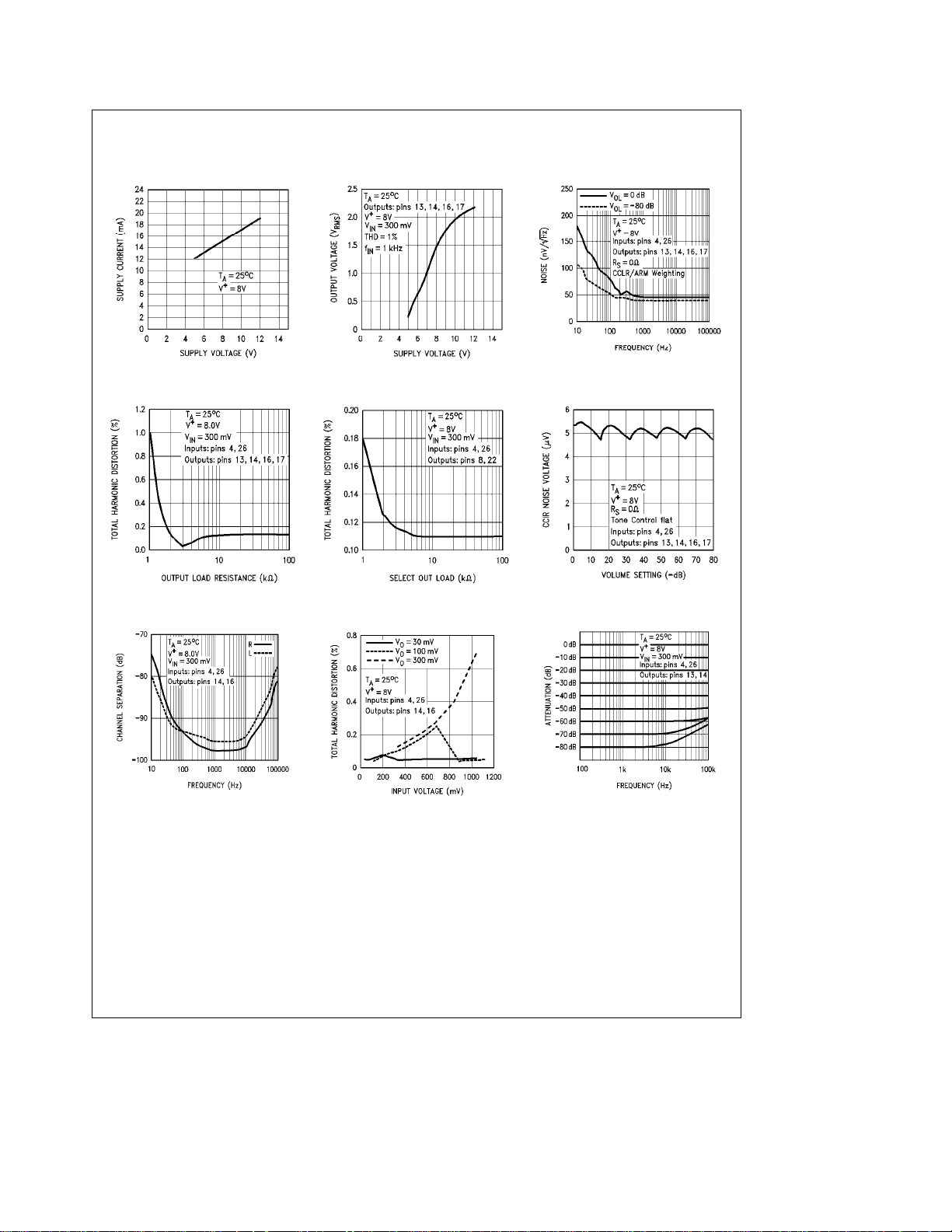
Typical Performance Characteristics
Quiescent Current vs
Supply Voltage
TL/H/10789– 3 TL/H/10789– 4
Total Harmonic Distortion
vs Output AC Load
TL/H/10789– 6 TL/H/10789– 7
Channel Separation
vs Frequency
Maximum Output Swing vs
Supply Voltage
Total Harmonic Distortion
vs Select Out AC Load
Total Harmonic Distortion
vs Input Voltage
Output Noise Voltage
vs Frequency
TL/H/10789– 5
CCIR Output Noise Voltage
vs Volume Setting
TL/H/10789– 8
Attenuation vs Frequency
TL/H/10789– 9
4
TL/H/10789– 10
TL/H/10789– 11
Page 5
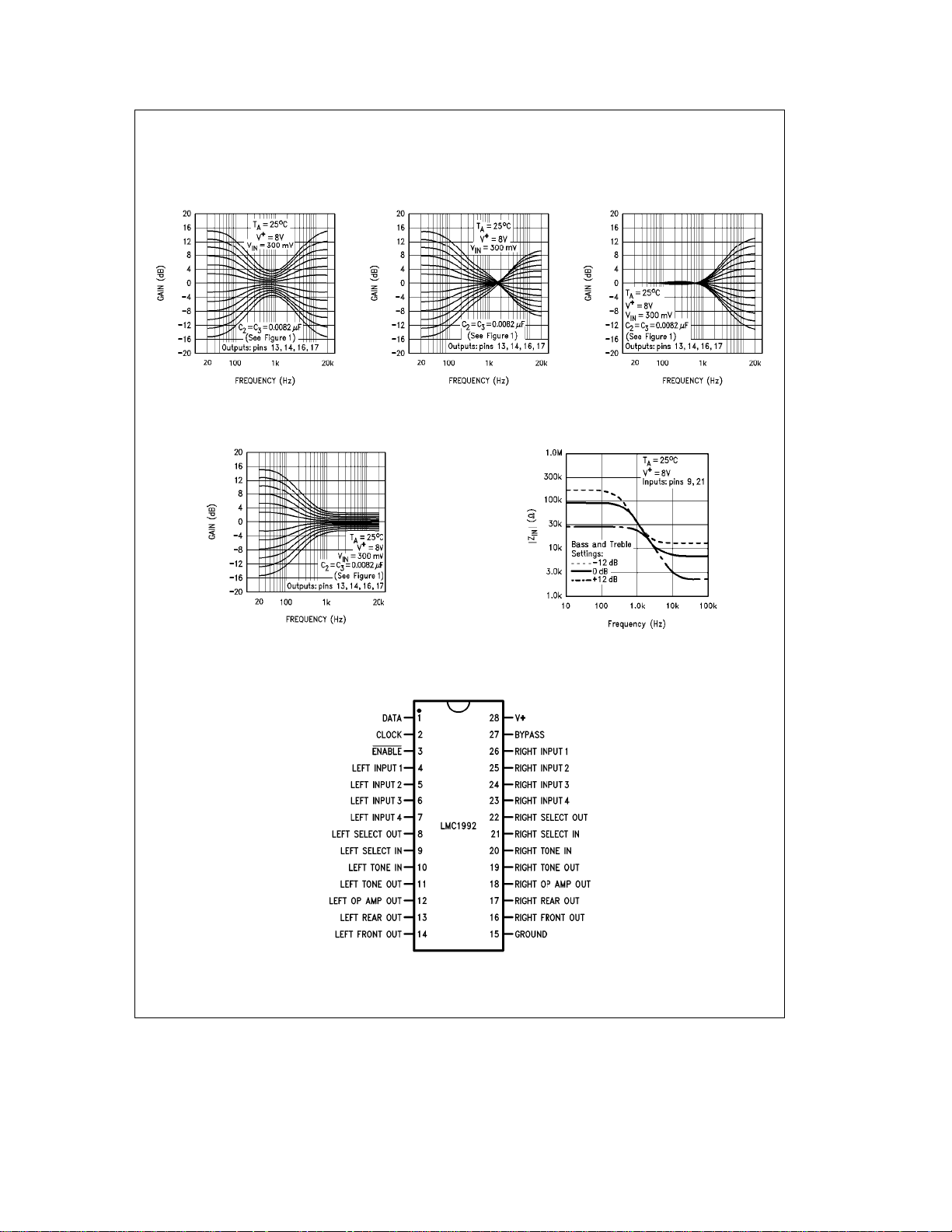
Typical Performance Characteristics (Continued)
Tone Control Response
with Equal Bass and
Treble Control Settings
TL/H/10789– 12 TL/H/10789– 13 TL/H/10789– 14
Bass Tone Control
Response
Tone Control Response
with Reciprocal Bass and
Treble Control Settings
Treble Tone Control
Response
Select In Impedance
vs Frequency
Connection Diagram
TL/H/10789– 15
TL/H/10789– 16
TL/H/10789– 17
5
Page 6

Pin Description
DATA(1) This is the serial data input for communica-
CLOCK(2) The CLOCK input accepts a TTL or CMOS
ENABLE
INPUT 1–4 Four two-channel analog inputs are available
(4–7, 23– 26) on the LMC1992. These pins should be dc-bi-
SELECT OUT The selected INPUT signal is available at this
(8, 22) output. This feature allows the use of external
SELECT IN This is the input that an external signal proc(9, 21) essor uses to return a signal to the LMC1992.
TONE IN This is the input to the tone control amplifier.
(10, 20) See the Application Information section titled
TONE OUT Tone control amplifier output. See the Appli(11, 19) cation Information section titled ‘‘Tone Con-
OP AMP OUT This output is used externally with the tone
(12, 18) control capacitors. Internally, this output is
tions sent by a controller. The data rate has a
maximum frequency of 500 kHz. The
LMC1992 requires 11 bits of data to control
or change a function: the first two bits, a 1
and 0, select the LMC1992, the next three
bits select a function, and the final six bits set
the function to a desired value. The data
must be valid on the rising edge of the
CLOCK input signal.
level clocking signal. The input is used to
clock the DATA input signal and determines
when a data bit is valid.
(3) This input accepts a logic low signal when a
controller is addressing the LMC1992. When
ENABLE
is active, the LMC1992 responds to
input signals present on the DATA and
CLOCK inputs.
ased to mid-supply.
signal processing such as noise reduction or
graphic equalizers. This output can typically
sink 1 mA.
‘‘Tone Control Response’’.
trol Response’’.
applied to the volume attenuators.
REAR OUT
(13, 17)
FRONT OUT This pin’s output signal is intended for the
(14, 16) front amplifiers in a four speaker stereo sys-
GROUND
(15) This is the system ground connection.
a
V
(28) This is the power supply connection. The
BYPASS (27) A 10 mF capacitor is connected between this
This pin’s output signal is intended for the
rear amplifiers in a four speaker stereo system. The output can typically sink 350 mA.
tem. The output can typically sink 350 mA.
LMC1992 is operational with supply voltages
from 6V to 12V. It is recommended that this
pin is bypassed with 0.1 mF capacitor.
pin and ground.
General Information
The LMC1992 is a CMOS/bipolar high quality building block
intended for high fidelity audio signal processing. It is designed for line level input signals (300 mV
maximum gain of
tured with CMOS processing, NPN transistors are used to
build low noise op amps. The combination of CMOS
switches, bipolar op amps, and SiCr resistors make it possible to achieve an order of magnitude quality improvement
over other bipolar circuits that use analog multipliers to accomplish gain adjustment.
The LMC1992 has internal decoding logic that allows a
computer (m P) to communicate directly to the audio control
circuitry through a standard MICROWIRE interface. This
three-wire interface consists of a DATA input line, a CLOCK
input line, and an ENABLE
low, data can be serially shifted from the controller to the
LMC1992. As the ENABLE
high transition, any additional data is ignored. Data present
in the internal shift register is latched and the instruction is
executed.
Figure 1
LMC1992 application.
b
1 dB. While the LMC1992 is manufac-
line. When the ENABLE line is
line goes through the low-to-
shows the connection diagram of a typical
b
2V) and has a
FIGURE 1. Typical Connection Diagram
6
TL/H/10789– 18
Page 7

Applications Information
MINIMUM LOAD IMPEDANCE
The LMC1992 employs emitter-follower buffers at pins 8
and 22 (SELECT OUT), 13 and 14 (LEFT FRONT and
REAR OUTPUTs), and 16 and 17 (RIGHT FRONT-andREAR OUTPUTs) that buffer output signals. Typical bias
current of 1 mA is used for the SELECT OUTPUT buffers
and 350 mA for the LEFT-and-RIGHT, FRONT-and-REAR
OUTPUT buffers.
The Electrical Specifications table lists a maximum input signal of 2.3 V
OUT pins. This distortion level is achieved when the minimum ac load impedance seen by the SELECT OUT pin is
3.25 kX (3.25V/1 mA). For the LEFT-and-RIGHT, FRONTand-REAR OUTPUTs, the typical maximum output is 1.2
V
(1.55 V
rms
is 4.43 kX (1.55 V/0.35 mA). Trying to use a lower impedance results in a clipped output signal. Therefore,
chance of clipping can be greatly reduced and much lower
distortion levels can be achieved by using load impedances
that are an order of magnitude higher than shown here.
For applications that require dc coupling and the INPUTs
biased to V
from that detailed in the above discussion. The emitter followers may be potentially operating at high currents because there is a dc voltage V
OUT pins; dc resistance to ground will result in increased
current flow. Latch-up may occur if the total emitter current
exceeds 5 mA. This current is a combination of the emitter
follower’s 1 mA current source and 4 mA drawn by the external load. Therefore, to prevent this possibility, the minimum dc load impedance should be
e
V
peak
a
e
V
To allow for variations and part tolerances, 2.0 kX is a good
choice for this minimum dc load impedance.
When dc coupling is used at the LEFT-and-RIGHT, FRONTand-REAR OUTPUTs, the output emitter followers will be
operating at a nominal dc voltage of V
Latch-up may occur if the total emitter current exceeds
1 mA. This current is a combination of the emitter follower’s
0.35 mA current source and 0.65 mA drawn by the external
load. Therefore, to prevent this possibility, the minimum dc
load impedance should be
e
V
peak
a
e
V
(3.25 V
rms
). Therefore, the minimum load impedance
peak
a
/2, the minimum load impedance will differ
V
peak
) for 1% THD at the SELECT
peak
a
/2b0.7V at the SELECT
a
(Va/2b0.7V)
4mA
e
1638X
3.25V
8V
a
a
V
(Va/2b2(0.7V))
peak
0.65 mA
e
9kX
3.25V
8V
the
/2b2(0.7V).
FIGURE 2. Input Bias Network
TL/H/10789– 20
To allow for variations and part tolerances, 10 kX is a good
choice for this minimum dc load impedance.
INPUT IMPEDANCE
For ac coupled input signals the input impedance value is
determined by bias resistor R1, as shown in
Figure 2.
directly coupled input signal will see an emitter follower’s
nominal input impedance of 2 MX.
The SELECT IN pins have an input impedance that varies
with the BASS and TREBLE control settings. The input impedance is 96 kX at dc and 27 kX at 1 kHz when the controls are set at 0 dB. Minimum input impedance of 28 kX at
dc and 24 kX at 1 kHz occurs when maximum boost is
selected. At 10 kHz the minimum input impedance, with the
tone controls flat, is 8 kX and, with the tone controls at
maximum boost, is 3 kX.
STEREO SIGNAL INPUTS
When operating with a single supply voltage, the stereo signal inputs must be dc biased to one-half of the supply voltage, as shown in
Figure 2.
As an example, with a supply
voltage of 8V, all signal sources should have a dc bias of
4V. The maximum input signal level of 6.5 V
THD) would then swing from 0.75V to 7.25V. Input-to-input
p-p
(for 1%
crosstalk can be minimized by using a separate dc bias circuit for each stereo input pair.
EXTERNAL SIGNAL PROCESSING
The signal present at the selected input will be available at
the SELECT OUT pins 8 (left) and 22 (right). The dc bias
voltage at those pins will be one base-emitter voltage, approximately 0.7 V
nal emitter follower. Therefore, if the selected input has a
bias of 4.0 V
about 3.3 V
, below the source because of the inter-
dc
the dc component at pins 8 and 22 will be
dc
.
dc
The LMC1992’s SELECT OUT emitter followers allow additional signal sources using emitter follower outputs (such as
multiple LMC1992s) to be ‘‘wired-ORed’’ together. When
this feature is in use, the input channel of the LMC1992 not
in use should be set to ‘‘open’’ input codes 01000XX0000 or
01000XX011X.
A
7
Page 8

Applications Information (Continued)
FIGURE 3. System Block Diagram Showing Inclusion of DNRÉNoise
Reduction (LM1894) and Equalizer (LMC835) (One Channel OnlyÐLMC1992)
The SELECT OUT pins (8 and 22) enable greater system
design flexibility by providing a means to implement an external processing loop. This loop can be used for noise reduction circuits such as DNR (LM1894) or mulit-band graphic equalizers (LMC835). It is important to ensure that if both
are used, the noise reduction circuitry precede the equalization circuits. Failure to do so will result in improper operation
of the noise reduction circuits. The system shown in
3
utilizes the external loop to include DNR and a multi-band
Figure
equalizer.
AUDIO MUTE
A mute function with attenuation of 100 dB is possible with
the volume control set to
b
80 dB and the INPUT select
code set to 01000XX0000 (open circuit).
TONE CONTROL RESPONSE
Base and treble tone controls are included in the LMC1992.
The tone controls use just two external capacitors for each
stereo channel. Each has a corner frequency determined by
the value of C2 and C3
(Figure 4)
and internal resistors in
the feedback loop of the internal tone amplifier. The maximum amplitude boost or cut is determined by the data sent
to the LMC1992 (see Table I).
TL/H/10789– 19
The typical tone control response shown in the Typical Performance Curves were generated with C2
eC3e
0.0082 mF and show the response for each step. When
modifying the tone control response it is important to note
that the ratio of C3 and C2 sets the mid-frequency gain.
Symmetrical tone response is achieved when C2
However, with C2
‘‘flat’’, the frequency response will be flat at 20 Hz and 20
kHz, and
a
e
2(C3) and the tone controls set to
6 dB at 1 kHz.
e
C3.
The frequency where a tone control begins to deviate from
a flat response will be referred to as the turn-over frequency. With C
eC2e
C3, the LMC1992’s treble turn-over
frequency is nominally
1
e
f
TT
2qC(14.2 kX)
The base turn-over frequency is nominally
1
e
f
BT
2qC(27.7 kX)
when maximum boost is chosen. The inflection points (the
frequencies where the boost or cut is within 3 dB of the final
value) are for treble and bass
1
e
f
TI
2qC(2.3 kX)
1
e
f
BI
2qC(164.1 kX)
8
Page 9

Applications Information (Continued)
FIGURE 4. The Tone Control Amplifier
Increasing the values of C2 and C3 decreases the turnover
and inflection frequencies: i.e., the Tone Control Response
Curves shown in Typical Performance Curves will shift left
when C2 and C3 are increased and shift right when C2 and
C3 are decreased. With C2
eC3e
0.0082, 2 dB steps are
achieved at 100 Hz and 10 kHz. Changing C2 and C3 to
0.01 mF shifts the 2 dB per step frequency to 72 Hz and 8.3
kHz. If the tone control capacitors’ size is decreased these
frequencies will increase. With C2
eC3e
dB steps take place at 130 Hz and 11.2 kHz.
FADER FUNCTION
The four fader functions are all independently adjustable
and therefore no balance control is needed. Emulating a
balance control is accomplished through software by simultaneously changing a channel’s front and rear faders by
equal amounts. To satisfy normal balance requirements the
faders have an attenuation range of 40 dB.
TL/H/10789– 22
0.0068 mF the 2
SERIAL COMMUNICATION INTERFACE
Figure 5
shows the LMC1992’s timing diagram for its three
wire MICROWIRE interface. A controller’s data stream can
be any length; once the correct device address is received
by the LMC1992, any number of data bits can be sent; the
last nine bits occurring before ENABLE
goes high are used
by the LMC1992. The first two bits in a valid data stream are
decoded and used as device address bits. The LMC1992
uses a unique address of 1,0. The LMC1992 will not respond to information on the DATA line if any other address
is used. This allows other MICROWIRE serially programmable devices to share the same three-wire communication
bus. When ENABLE
goes high, any further serial data is
ignored and the contents of the shift register is transferred
to the data latches. Only when information is received by
the data latches do any function or setting changes take
place. The first three of nine bits select one of the
LMC1992s functions. The remaining six bits set the selected function to the desired value or position.
A data bit is accepted as valid and clocked into an internal
shift register on each rising edge of the signal appearing at
the LMC1992s CLOCK input pin. Proper data interpretation
and operation is ensured when ENABLE
makes its falling
transition during the time when CLOCK is low. Erroneous
operation will result if the ENABLE
signal makes its falling
transition at any other time.
Note 1: Negative transition on ENABLE clears previous address. Clock must be low during transition.
Note 2: Additional don’t care states may be inserted here for ease of programming. (Optional.)
Note 3: Positive transition on ENABLE
latches in new data if the LMC1992 has been addressed. Clock can either be high or low during transition.
FIGURE 5. Clocking Data into the Standard MICROWIRE Interface
(Minimum Number of Bits in Data Stream)
9
TL/H/10789– 21
Page 10

Applications Information (Continued)
TABLE I. Programming Codes for LMC1992
Address
A2 A1 A0 D5 D4 D3 D2 D1 D0
Function
1 1 1 Left Rear Fader X MSB N N N LSB
1 1 0 Right Rear Fader X MSB N N N LSB
1 0 1 Left Front Fader X MSB N N N LSB
1 0 0 Right Front Fader X MSB N N N LSB
0 1 1 Volume MSB N N N N LSB
0 1 0 Treble X X MSB N N LSB
0 0 1 Bass X X MSB N N LSB
0 0 0 Input Select X X 0 MSB N LSB OPENeXX0000
Note 1: All attenuators 2 dB/step.
Note 2: Tone controls 2 dB/step
Note 3: Use of data that deviates from the values shown in the table may result in erroneous results.
@
100 Hz and 10 kHz.
SERIAL DATA FORMAT
Table I displays the required data format needed by the
LMC1992. Not shown is the 2-bit device address (10).
These two bits of information must precede the final ninebits used as the data word. The first three of these nine bits
is the function address.
The VOLUME, TONE, and FADER controls are designed to
increment their settings (in 2 dB steps) as the control data is
incremented by one LSB. Disregarding the device address
and the function address, the VOLUME input code increases from 000000 (
b
80 dB) to 10100X (0 dB). The TONE
Data
Values
b
40 dBeX00000
b
20 dBeX01010
e
0dB
X1010X
b
40 dBeX00000
b
20 dBeX01010
e
0dB
X1010X
b
40 dBeX00000
b
20 dBeX01010
e
0dB
X1010X
b
40 dBeX00000
b
20 dBeX01010
0dBeX1010X
b
80 dBe000000
b
40 dBe010100
e
0dB
10100X
b
12 dBeXX0000
e
FLAT
a
b
a
INPUT1
INPUT2
INPUT3
XX0110
12 dBeXX1100
12 dBeXX0000
e
FLAT
XX0110
12 dBeXX1100
e
XX0001
e
XX0010
e
XX0011
INPUT4eXX0100
b
controls’ input code increases from XX0000 (
XX0110 (0 dB) to XX1100 (
ERs starts from X00000 (
a
12 dB). The code for the FAD-
b
40 dB) and goes to X1010X
12 dB) to
(0 dB).
The table shows that VOLUME is the only function that uses
all six bits to choose that function’s setting. The remaining
functions use less than six bits; the unused bits are shown
as ‘‘X’’s (‘‘don’t care’’). While these ‘‘don’t care’’ bits have
no effect on their respective function, the LMC1992 must
receive them for proper operation. If neglected, erroneous
or unknown results will occur.
10
Page 11

Applications Information (Continued)
DATA TRANSFER EXAMPLE
The following routines, based on the flowchart shown in
ure 6,
are examples of COPSTMmicrocontroller instruction
code that can be used to control the LMC1992 (see National Semiconductor’s COPS Microcontrollers Databook for
more information). These routines arbitrarily select COPS
register 0 for I/O purposes. When these routines are entered, it is assumed that chip select is high, SK (clock) is
low, and SO (data) is low. These routines exit with chip select high and SK and SO low. Output port G0 is arbitrarily
chosen to send the chip select signal to the LMC1992.
The 11 data bits needed to control the LMC1992 are assumed to be in the 4-bit registers, 13 – 15, with the 4 MSBs
in register 13. With this configuration there is an extra bit for
a data stream that is 12 bits long. As previously mentioned,
there can be any number of extra bits between the device
address and the function address.
DATA TRANSFER ROUTINE 1
This general purpose routine handles all the overhead except loading data into registers 13 – 15. It sends the data
according to the conditions discussed above. The data will
be lost at the conclusion of the routine. This routine consumes only 17 ROM memory locations.
OUT1: LBI 0,13 ;POINT TO START OF DATA
SC ;SET C TO ENABLE SK CLOCK
OGI 14 ;SELECT EXTERNAL DEVICE G0
LEI 8 ;ENABLE SHIFT REGISTER
SEND: LD
XAS ;DATA TRANSMISSION LOOP
XIS ;TURN-ON CLOCK
JP SEND
RC
OGI 15 ;DE-SELECT EXTERNAL
LEI 0 ;SET S0 TO 0
RET
;WORD
;4 0
;OUTPUT
DEVICE
Fig-
DATA TRANSFER ROUTINE 2
This routine performs the same function as routine 1 while
preserving the contents of the data registers. This routine
takes only 21 ROM memory locations.
OUT1: LBI 0,13 ;POINT TO START OF DATA
;WORD
SC ;SET C TO ENABLE SK CLOCK
OGI 14 ;SELECT EXTERNAL DEVICE
GO ;40
LEI 8 ;ENABLE SHIFT REGISTER
;OUTPUT
JP SEND2
SEND1: XAS
SEND2: LD ;DATA TRANSMISSION LOOP
XIS ;TURN-ON CLOCK
JP SEND1
XAS ;SEND LAST DATA
RC ;WAIT 4 CYCLES - DATA
;GOING OUT
CLRA
NOP
XAS ;TURN SK CLOCK OFF
OGI 15 ;DE-SELECT DEVICE
LEI 0 ;SET S0 TO 0
RET
11
Page 12

Applications Information (Continued)
FIGURE 6. General Data Transmission Flowchart to Send Serial Data
to the LMC1992’s MICROWIRE Compatible Digital Inputs
12
TL/H/10789– 23
Page 13

13
Page 14

Physical Dimensions inches (millimeters)
LMC1992 Digitally-Controlled Stereo Tone and
Volume Circuit with Four-Channel Input Selector
Molded Dual-In-Line Package (N)
Order Number LMC1992CCN
NS Package Number N28B
LIFE SUPPORT POLICY
NATIONAL’S PRODUCTS ARE NOT AUTHORIZED FOR USE AS CRITICAL COMPONENTS IN LIFE SUPPORT
DEVICES OR SYSTEMS WITHOUT THE EXPRESS WRITTEN APPROVAL OF THE PRESIDENT OF NATIONAL
SEMICONDUCTOR CORPORATION. As used herein:
1. Life support devices or systems are devices or 2. A critical component is any component of a life
systems which, (a) are intended for surgical implant support device or system whose failure to perform can
into the body, or (b) support or sustain life, and whose be reasonably expected to cause the failure of the life
failure to perform, when properly used in accordance support device or system, or to affect its safety or
with instructions for use provided in the labeling, can effectiveness.
be reasonably expected to result in a significant injury
to the user.
National Semiconductor National Semiconductor National Semiconductor National Semiconductor National Semiconductores National Semiconductor
Corporation GmbH Japan Ltd. Hong Kong Ltd. Do Brazil Ltda. (Australia) Pty, Ltd.
2900 Semiconductor Drive Livry-Gargan-Str. 10 Sumitomo Chemical 13th Floor, Straight Block, Rue Deputado Lacorda Franco Building 16
P.O. Box 58090 D-82256 F4urstenfeldbruck Engineering Center Ocean Centre, 5 Canton Rd. 120-3A Business Park Drive
Santa Clara, CA 95052-8090 Germany Bldg. 7F Tsimshatsui, Kowloon Sao Paulo-SP Monash Business Park
Tel: 1(800) 272-9959 Tel: (81-41) 35-0 1-7-1, Nakase, Mihama-Ku Hong Kong Brazil 05418-000 Nottinghill, Melbourne
TWX: (910) 339-9240 Telex: 527649 Chiba-City, Tel: (852) 2737-1600 Tel: (55-11) 212-5066 Victoria 3168 Australia
National does not assume any responsibility for use of any circuitry described, no circuit patent licenses are implied and National reserves the right at any time without notice to change said circuitry and specifications.
Fax: (81-41) 35-1 Ciba Prefecture 261 Fax: (852) 2736-9960 Telex: 391-1131931 NSBR BR Tel: (3) 558-9999
Tel: (043) 299-2300 Fax: (55-11) 212-1181 Fax: (3) 558-9998
Fax: (043) 299-2500
 Loading...