

Page 1
LM98714
Three Channel, 16-Bit, 45 MSPS Digital Copier Analog
Front End with Integrated CCD/CIS Sensor Timing
Generator and LVDS Output
General Description
The LM98714 is a fully integrated, high performance 16-Bit,
45 MSPS signal processing solution for digital color copiers,
scanners, and other image processing applications. Highspeed signal throughput is achieved with an innovative architecture utilizing Correlated Double Sampling (CDS), typically employed with CCD arrays, or Sample and Hold (S/H)
inputs (for Contact Image Sensors and CMOS image sensors). The signal paths utilize 8 bit Programmable Gain
Amplifiers (PGA), a +/-9-Bit offset correction DAC and independently controlled Digital Black Level correction loops for
each input. The PGA and offset DAC are programmed independently allowing unique values of gain and offset for each
of the three inputs. The signals are then routed to a 45MHz
high performance analog-to-digital converter (ADC). The
fully differential processing channel shows exceptional noise
immunity, having a very low noise floor of -74dB. The 16-bit
ADC has excellent dynamic performance making the
LM98714 transparent in the image reproduction chain.
Applications
n Multi-Function Peripherals
n Facsimile Equipment
n Flatbed or Handheld Color Scanners
n High-speed Document Scanner
Features
n LVDS/CMOS Outputs
n LVDS/CMOS Pixel Rate Input Clock or ADC Input Clock
n CDS or S/H Processing for CCD or CIS sensors
n Independent Gain/Offset Correction for Each Channel
n Digital Black Level Correction Loop for Each Channel
n Programmable Input Clamp Voltage
n Flexible CCD/CIS Sensor Timing Generator
Key Specifications
n Maximum Input Level 1.2 or 2.4 Volt Modes
n (both with + or - polarity option)
n ADC Resolution 16-Bit
n ADC Sampling Rate 45 MSPS
n INL +/- 23 LSB (typ)
n Channel Sampling Rate 15/22.5/30 MSPS
n PGA Gain Steps 256 Steps
n PGA Gain Range 0.7 to 7.84x
n Analog DAC Resolution +/-9 Bits
n Analog DAC Range +/-300mV or +/-600mV
n Digital DAC Resolution +/-6 Bits
n Digital DAC Range -1024 LSB to + 1008 LSB
n SNR -74dB (
@
0dB PGA Gain)
n Power Dissipation 505mW (LVDS) 610mW (CMOS)
n Operating Temp 0 to 70˚C
n Supply Voltage 3.3V Nominal (3.0V to 3.6V range)
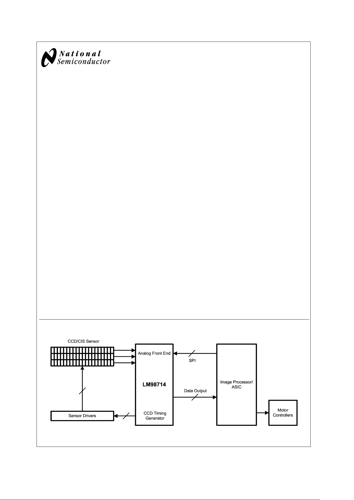
System Block Diagram
20105370
October 2006
LM98714 - Three Channel, 16-Bit, 45 MSPS Digital Copier Analog Front End with Integrated
CCD/CIS Sensor Timing Generator and LVDS Output
© 2006 National Semiconductor Corporation DS201053 www.national.com
Page 2
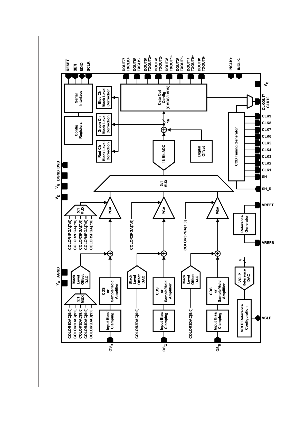
LM98714 Overall Chip Block Diagram
20105301
FIGURE 1. Chip Block Diagram
LM98714
www.national.com 2
Page 3
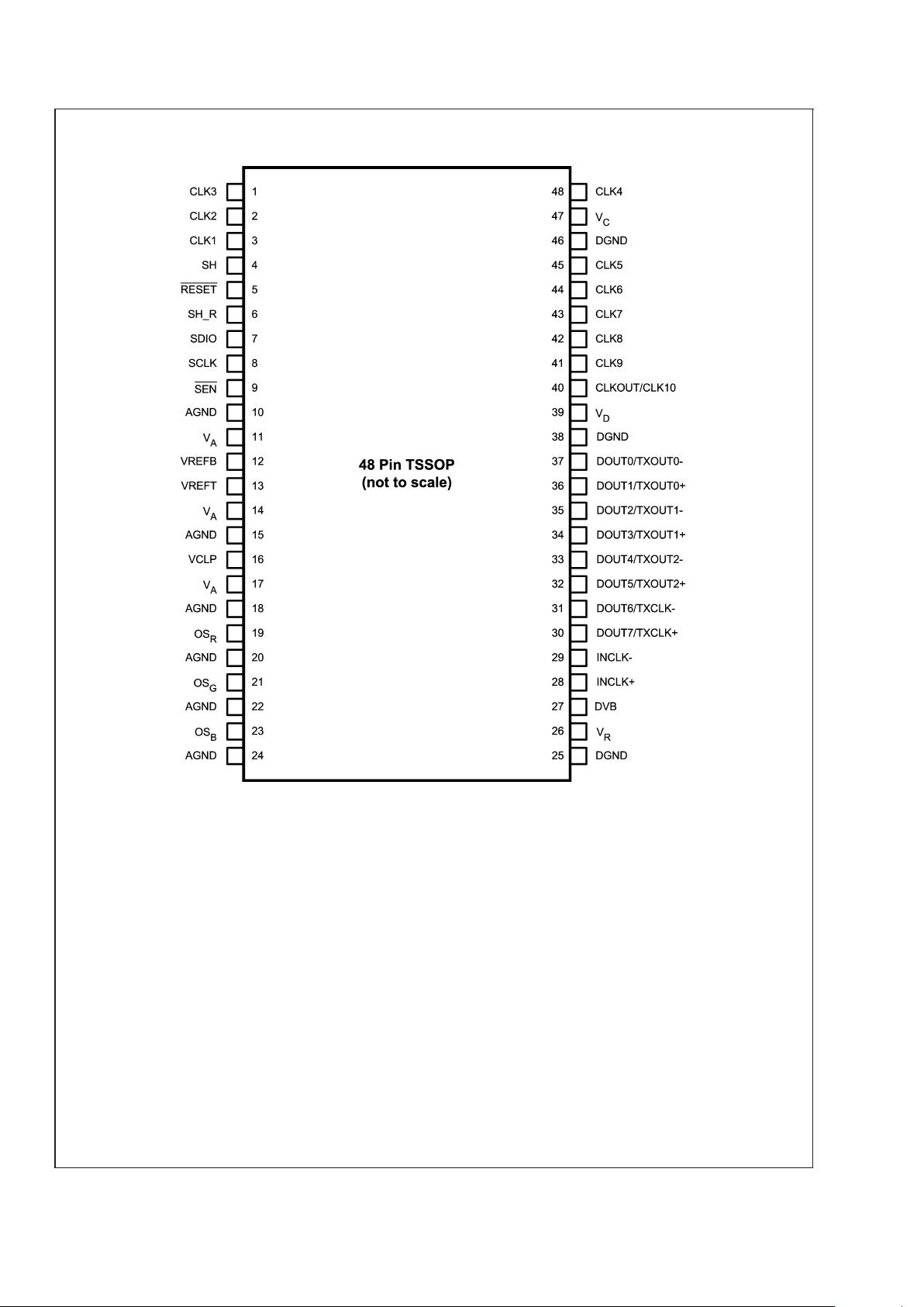
LM98714 Pin Out Diagram
20105302
FIGURE 2. LM98714 Pin Out Diagram
LM98714
www.national.com3
Page 4
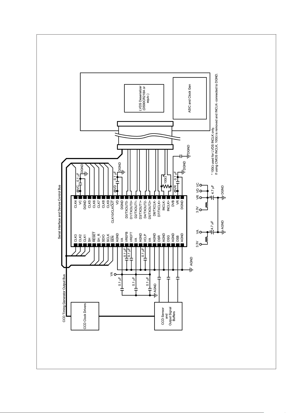
Typical Application Diagram
20105373
FIGURE 3. Typical Application Diagram
LM98714
www.national.com 4
Page 5

Pin Descriptions
Pin Name I/O Typ Res Description
1 CLK3 O D PU Configurable sensor control output.
2 CLK2 O D PD Configurable sensor control output.
3 CLK1 O D PU Configurable sensor control output.
4 SH O D PD Sensor - Shift or transfer control signal for CCD and CIS sensors.
5 RESET
I D PU Active-low master reset. NC when function not being used.
6 SH_R I D PD External request for an SH pulse.
7 SDIO I/O D Serial Interface Data Input
8 SCLK I D PD Serial Interface shift register clock.
9 SEN
I D PU Active-low chip enable for the Serial Interface.
10 AGND P Analog ground return.
11 V
A
P Analog power supply. Bypass voltage source with 4.7µF and pin with 0.1µF to
AGND.
12 VREFB O A Bottom of ADC reference. Bypass with a 0.1µF capacitor to ground.
13 VREFT O A Top of ADC reference. Bypass with a 0.1µF capacitor to ground.
14 V
A
P Analog power supply. Bypass voltage source with 4.7µF and pin with 0.1µF to
AGND.
15 AGND P Analog ground return.
16 VCLP IO A Input Clamp Voltage. Normally bypassed with a 0.1µF, and a 4.7µF capacitor to
AGND. An external reference voltage may be applied to this pin.
17 V
A
P Analog power supply. Bypass voltage source with 4.7µF and pin with 0.1µF to
AGND.
18 AGND P Analog ground return.
19 OS
R
I A Analog input signal. Typically sensor Red output AC-coupled thru a capacitor.
20 AGND P Analog ground return.
21 OS
G
I A Analog input signal. Typically sensor Green output AC-coupled thru a capacitor.
22 AGND P Analog ground return.
23 OS
B
I A Analog input signal. Typically sensor Blue output AC-coupled thru a capacitor.
24 AGND P Analog ground return.
25 DGND P Digital ground return.
26 V
R
P Power supply input for internal voltage reference generator. Bypass this supply
pin with a 0.1µF capacitor.
27 DVB O P Digital Core Voltage bypass. Not an input. Bypass with 0.1µF capacitor to
DGND.
28 INCLK+ I D Clock Input. Non-Inverting input for LVDS clocks or CMOS clock input. CMOS
clock is selected when pin 29 is held at DGND, otherwise clock is configured
for LVDS operation.
29 INCLK- I D Clock Input. Inverting input for LVDS clocks, connect to DGND for CMOS clock.
30 DOUT7/ O D Bit 7 of the digital video output bus in CMOS Mode, LVDS Frame Clock+ in
LVDS Mode.
TXCLK+
31 DOUT6/ O D Bit 6 of the digital video output bus in CMOS Mode, LVDS Frame Clock- in
LVDS Mode.
TXCLK-
32 DOUT5/ O D Bit 5 of the digital video output bus in CMOS Mode, LVDS Data Out2+ in LVDS
Mode.
TXOUT2+
33 DOUT4/ O D Bit 4 of the digital video output bus in CMOS Mode, LVDS Data Out2- in LVDS
Mode.
TXOUT2-
34 DOUT3/ O D Bit 3 of the digital video output bus in CMOS Mode, LVDS Data Out1+ in LVDS
Mode.
TXOUT1+
35 DOUT2/ O D Bit 2 of the digital video output bus in CMOS Mode, LVDS Data Out1- in LVDS
Mode.
TXOUT1-
LM98714
www.national.com5
Page 6

Pin Descriptions (Continued)
Pin Name I/O Typ Res Description
36 DOUT1/ O D Bit 1 of the digital video output bus in CMOS Mode, LVDS Data Out0+ in LVDS
Mode.
TXOUT0+
37 DOUT0/ O D Bit 0 of the digital video output bus in CMOS Mode, LVDS Data Out0- in LVDS
Mode.
TXOUT0-
38 DGND P Digital ground return.
39 V
D
P Power supply for the digital circuits. Bypass this supply pin with 0.1µF
capacitor. A single 4.7µF capacitor should be used between the supply and the
VD, VR and VC pins.
40 CLKOUT/
CLK10
O D PD Output clock for registering output data when using CMOS outputs, or
configurable sensor control output.
41 CLK9 O D PD Configurable sensor control output.
42 CLK8 O D PD Configurable sensor control output.
43 CLK7 O D PD Configurable sensor control output.
44 CLK6 O D PU Configurable sensor control output.
45 CLK5 O D PD Configurable sensor control output.
46 DGND P Digital ground return.
47 V
C
P Power supply for the sensor control outputs. Bypass this supply pin with 0.1µF
capacitor.
48 CLK4 O D PD Configurable sensor control output.
(I=Input), (O=Output), (IO=Bi-directional), (P=Power), (D=Digital), (A=Analog), (PU=Pull Up with an internal resistor), (PD=Pull Down with an internal resistor.).
LM98714
www.national.com 6
Page 7

Absolute Maximum Ratings (Notes 2,
1)
If Military/Aerospace specified devices are required,
please contact the National Semiconductor Sales Office/
Distributors for availability and specifications.
Supply Voltage (VA,VR,VD,VC) 4.2V
Voltage on Any Input Pin
(Not to exceed 4.2V)
−0.3V to
(VA + 0.3V)
Voltage on Any Output Pin
(execpt DVB and not to exceed
4.2V)
−0.3V to
(VA + 0.3V)
DVB Output Pin Voltage 2.0V
Input Current at any pin other than
Supply Pins (Note 3)
±
25 mA
Package Input Current (except
Supply Pins) (Note 3)
±
50 mA
Maximum Junction Temperature (TA) 150˚C
Thermal Resistance (θ
JA
) 66˚C/W
Package Dissipation at T
A
= 25˚C
(Note 4)
1.89W
ESD Rating (Note 5)
Human Body Model 2500V
Machine Model 250V
Storage Temperature −65˚C to +150˚C
Soldering process must comply with National
Semiconductor’s Reflow Temperature Profile
specifications. Refer to www.national.com/packaging.
(Note 6)
Operating Ratings (Notes 1, 2)
Operating Temperature Range 0˚C ≤ T
A
≤ +70˚C
All Supply Voltage +3.0V to +3.6V
Electrical Characteristics
The following specifications apply for VA = VD = VR = VC = 3.3V, CL= 10pF, and f
INCLK
= 15MHz unless otherwise specified.
Boldface limits apply for T
A=TMIN
to T
MAX
; all other limits TA= 25˚C.
Symbol Parameter Conditions Min
Typ
(Note 8) Max Units
CMOS Digital Input DC Specifications (RESETb, SH_R, SCLK, SENb)
V
IH
Logical “1” Input Voltage 2.0 V
V
IL
Logical “0” Input Voltage 0.8 V
I
IH
Logical “1” Input Current VIH=VD
RESET
235 nA
SH_R, SCLK 70 µA
SEN
130 nA
I
IL
Logical “0” Input Current VIL = DGND
RESET
70 µA
SH_R, SCLK 235 nA
SEN
70 µA
CMOS Digital Output DC Specifications (SH, CLK1 to CLK10, CMOS Data Outputs)
V
OH
Logical “1” Output Voltage I
OUT
= -0.5mA 2.95 V
V
OL
Logical “0” Output Voltage I
OUT
= 1.6mA 0.25 V
I
OS
Output Short Circuit Current V
OUT
= DGND 16 mA
V
OUT
= VD -20
I
OZ
CMOS Output TRI-STATE
Current
V
OUT
= DGND 20 nA
V
OUT
= VD -25
CMOS Digital Input/Output DC Specifications (SDIO)
I
IH
Logical “1” Input Current VIH=VD 90 nA
I
IL
Logical “0” Input Current VIL= DGND 90 nA
LVDS/CMOS Clock Receiver DC Specifications (INCLK+ and INCLK- Pins)
V
IHL
Differential LVDS Clock RL= 100W 100 mV
High Threshold Voltage V
CM
(LVDS Input Common
Mode Voltage)= 1.25V
V
ILL
Differential LVDS Clock -100 mV
Low Threshold Voltage
LM98714
www.national.com7
Page 8

Electrical Characteristics (Continued)
The following specifications apply for VA = VD = VR = VC = 3.3V, CL= 10pF, and f
INCLK
= 15MHz unless otherwise specified.
Boldface limits apply for T
A=TMIN
to T
MAX
; all other limits TA= 25˚C.
Symbol Parameter Conditions Min
Typ
(Note 8) Max Units
V
IHC
CMOS Clock INCLK- = DGND 2.0 V
High Threshold Voltage
V
ILC
CMOS Clock 0.8 V
Low Threshold Voltage
I
IHL
CMOS Clock 280 µA
Input High Current
I
ILC
CMOS Clock -150 µA
Input Low Current
LVDS Output DC Specifications
V
OD
Differential Output Voltage RL= 100Ω 180 328 450 mV
V
OS
LVDS Output Offset Voltage 1.17 1.23 1.3 V
I
OS
Output Short Circuit Current V
OUT
= 0V, RL= 100Ω 7.9 mA
Power Supply Specifications
IA VA Analog Supply Current VA Normal State 60 97 125 mA
VA Low Power State 12 23 32 mA
(Powerdown)
IR VR Digital Supply Current VR Normal State 30 64 75 mA
(LVDS Outputs)
CMOS Output Data Format 15 47 55 mA
LVDS Output Data Format
with Data Outputs Disabled
47 mA
ID VD Digital Output Driver Supply LVDS Output Data Format 0.05 mA
Current CMOS Output Data Format 12 40 mA
(ATE Loading of CMOS
Outputs
>
50pF)
IC VC CCD Timing Generator
Output Driver Supply Current
Typical sensor outputs: 0.5 12 mA
SH, CLK1=Φ1A, CLK2=Φ2A,
CLK3=ΦB, CLK4=ΦC,
CLK5=RS, CLK6=CP
(ATE Loading of CMOS
Outputs
>
50pF)
PWR Average Power Dissipation LVDS Output Data Format 350 505 650 mW
CMOS Output Data Format 380 610 700 mW
(ATE Loading of CMOS
Outputs
>
50pF)
Input Sampling Circuit Specifications
V
IN
Input Voltage Level CDS Gain=1x, PGA Gain=1x 2.3 Vp-p
CDS Gain=2x, PGA Gain=
1x
1.22
LM98714
www.national.com 8
Page 9

Electrical Characteristics (Continued)
The following specifications apply for VA = VD = VR = VC = 3.3V, CL= 10pF, and f
INCLK
= 15MHz unless otherwise specified.
Boldface limits apply for T
A=TMIN
to T
MAX
; all other limits TA= 25˚C.
Symbol Parameter Conditions Min
Typ
(Note 8) Max Units
I
IN_SH
Sample and Hold Mode Source Followers Off 50 70 µA
Input Leakage Current CDS Gain = 1x (-70) (-40)
OS
X
=VA(OSX= AGND)
Source Followers Off 75 105 µA
CDS Gain = 2x (-105) (-75)
OS
X
=VA(OSX= AGND)
Source Followers On -200 -10 200 nA
CDS Gain = 2x -16
OS
X
=VA(OSX= AGND)
C
SH
Sample/Hold Mode CDS Gain = 1x 2.5 pF
Equivalent Input Capacitance
(see Figure 11) CDS Gain = 2x 4 pF
I
IN_CDS
CDS Mode Source Followers Off -300 7 300 nA
Input Leakage Current OS
X
=VA(OSX= AGND) (-25)
R
CLPIN
CLPIN Switch Resistance 16 50 Ω
(OS
X
to VCLP Node in Figure 8)
VCLP Reference Circuit Specifications
VCLP DAC Resolution 4 Bits
VCLP DAC Step Size 0.16 V
V
VCLP
VCLP DAC Voltage Min Output VCLP Config. Register = 0.14 0.26 0.43 V
0001 0000b
VCLP DAC Voltage Max Output VCLP Config. Register = 2.38 2.68 2.93 V
0001 1111b
Resistor Ladder Enabled VCLP Config. Register = 1.54 V
A
/ 2 1.73 V
0010 xxxxb
I
SC
VCLP DAC Short Circuit Output
Current
VCLP Config. Register = 30 mA
0001 xxxxb
Black Level Offset DAC Specifications
Resolution 10 Bits
Monotonicity Guaranteed by characterization
Offset Adjustment Range CDS Gain = 1x
mV
Referred to AFE Input Minimum DAC Code =
0x000
-614
Maximum DAC Code =
0x3FF
614
CDS Gain = 2x
mV
Minimum DAC Code =
0x000
-307
Maximum DAC Code =
0x3FF
307
Offset Adjustment Range Minimum DAC Code =
0x000
-16000 -18200
LSB
Referred to AFE Output Maximum DAC Code =
0x3FF
16000 18200
DAC LSB Step Size CDS Gain = 1x 1.2 mV
Referred to AFE Output (32) (LSB)
DNL Differential Non-Linearity -0.95 3.25 LSB
LM98714
www.national.com9
Page 10

Electrical Characteristics (Continued)
The following specifications apply for VA = VD = VR = VC = 3.3V, CL= 10pF, and f
INCLK
= 15MHz unless otherwise specified.
Boldface limits apply for T
A=TMIN
to T
MAX
; all other limits TA= 25˚C.
Symbol Parameter Conditions Min
Typ
(Note 8) Max Units
INL Integral Non-Linearity -3.1 2.65 LSB
PGA Specifications
Gain Resolution 8 Bits
Monotonicity Guaranteed by characterization
Maximum Gain CDS Gain = 1x 7.18 7.9 8.77 V/V
CDS Gain = 1x 17.1 17.9 18.9 dB
Minimum Gain CDS Gain = 1x 0.56 0.7 0.82 V/V
CDS Gain = 1x -5 -3 -1.72 dB
PGA Function Gain (V/V) = (196/(280-PGA Code))
Gain (dB) = 20LOG10(196/(280-PGA Code))
Channel Matching Minimum PGA Gain 3 %
Maximum PGA Gain 12.7
ADC Specifications
V
REFT
Top of Reference 2.07 V
V
REFB
Bottom of Reference 0.89 V
V
REFT
-
V
REFB
Differential Reference Voltage 1.07 1.18 1.29 V
Overrange Output Code 65535
Underrange Output Code 0
Digital Offset “DAC” Specifications
Resolution 7 Bits
Digital Offset DAC LSB Step Size Referred to AFE Output 16 LSB
Offset Adjustment Range Min DAC Code =7b0000000 -1024
LSB
Referred to AFE Output Mid DAC Code =7b1000000 0
Max DAC Code =
7b1111111
1008
Full Channel Performance Specifications
DNL Differential Non-Linearity -0.99 0.8/-0.6 2.55 LSB
INL Integral Non-Linearity -73 +/-23 78 LSB
SNR Total Output Noise Minimum PGA Gain -79 dB
7.2 LSB
RMS
PGA Gain = 1x -74 dB
13 30 LSB
RMS
Maximum PGA Gain -56 dB
104 LSB
RMS
Channel to Channel Crosstalk Mode 3 47
LSB
Mode 2 16
Note 1: Absolute Maximum Ratings indicate limits beyond which damage to the device may occur. Operating Ratings indicate conditions for which the device is
functional, but do not guarantee specific performance limits. For guaranteed specifications and test conditions, see the Electrical Characteristics. The guaranteed
specifications apply only for the test conditions listed. Some performance characteristics may degrade when the device is not operated under the listed test
conditions. Operation of the device beyond the Operating Ratings is not recommended.
Note 2: All voltages are measured with respect to AGND = DGND = 0V, unless otherwise specified.
Note 3: When the input voltage (V
IN
) at any pin exceeds the power supplies (V
IN
<
GND or V
IN
>
VAor VD), the current at that pin should be limited to 25 mA.
The 50 mA maximum package input current rating limits the number of pins that can simultaneously safely exceed the power supplies with an input current of 25
mA to two.
LM98714
www.national.com 10
Page 11

Note 4: The maximum power dissipation must be derated at elevated temperatures and is dictated by T
JMAX
, θJAand the ambient temperature, TA. The maximum
allowable power dissipation at any temperature is P
D
=(T
JMAX–TA
)/θJA. The values for maximum power dissipation listed above will be reached only when the
device is operated in a severe fault condition (e.g. when input or output pins are driven beyond the power supply voltages, or the power supply polarity is reversed).
Such conditions should always be avoided.
Note 5: Human body model is 100 pF capacitor discharged through a 1.5 kΩ resistor. Machine model is 220 pF discharged through 0Ω.
Note 6: Reflow temperature profiles are different for lead-free and non-lead-free packages.
Note 7: The analog inputs are protected as shown below. Input voltage magnitudes beyond the supply rails will not damage the device, provided the current is
limited per note 3. However, input errors will be generated If the input goes above VA and below AGND.
20105371
Note 8: Typical figures are at TA= 25˚C, and represent most likely parametric norms at the time of product characterization. The typical specifications are not
guaranteed.
LM98714
www.national.com11
Page 12

Physical Dimensions inches (millimeters) unless otherwise noted
48-Lead TSSOP
NS Package Number MTD48
National does not assume any responsibility for use of any circuitry described, no circuit patent licenses are implied and National reserves
the right at any time without notice to change said circuitry and specifications.
For the most current product information visit us at www.national.com.
LIFE SUPPORT POLICY
NATIONAL’S PRODUCTS ARE NOT AUTHORIZED FOR USE AS CRITICAL COMPONENTS IN LIFE SUPPORT DEVICES OR SYSTEMS
WITHOUT THE EXPRESS WRITTEN APPROVAL OF THE PRESIDENT AND GENERAL COUNSEL OF NATIONAL SEMICONDUCTOR
CORPORATION. As used herein:
1. Life support devices or systems are devices or systems
which, (a) are intended for surgical implant into the body, or
(b) support or sustain life, and whose failure to perform when
properly used in accordance with instructions for use
provided in the labeling, can be reasonably expected to result
in a significant injury to the user.
2. A critical component is any component of a life support
device or system whose failure to perform can be reasonably
expected to cause the failure of the life support device or
system, or to affect its safety or effectiveness.
BANNED SUBSTANCE COMPLIANCE
National Semiconductor follows the provisions of the Product Stewardship Guide for Customers (CSP-9-111C2) and Banned Substances
and Materials of Interest Specification (CSP-9-111S2) for regulatory environmental compliance. Details may be found at:
www.national.com/quality/green.
Lead free products are RoHS compliant.
National Semiconductor
Americas Customer
Support Center
Email: new.feedback@nsc.com
Tel: 1-800-272-9959
National Semiconductor
Europe Customer Support Center
Fax: +49 (0) 180-530 85 86
Email: europe.support@nsc.com
Deutsch Tel: +49 (0) 69 9508 6208
English Tel: +44 (0) 870 24 0 2171
Français Tel: +33 (0) 1 41 91 8790
National Semiconductor
Asia Pacific Customer
Support Center
Email: ap.support@nsc.com
National Semiconductor
Japan Customer Support Center
Fax: 81-3-5639-7507
Email: jpn.feedback@nsc.com
Tel: 81-3-5639-7560
www.national.com
LM98714 - Three Channel, 16-Bit, 45 MSPS Digital Copier Analog Front End with Integrated
CCD/CIS Sensor Timing Generator and LVDS Output
 Loading...