

Page 1
LM98501
10-Bit, 27 MSPS Camera Signal Processor
General Description
The LM98501 is a CCD signal processor for electronic cameras. The processor provides a common interface to a number of different image sensors including CCD, CMOS, and
CIS. Correlated double sampling reduces kTC noise from
the image signal. A fast, temperature stable, 8-bit digitally
programmable gain amplifier enables pixel-rate
white-balancing. An auxiliary input is provided, allowing for
the selection of anexternalsignal, useful for electronic titling
and video overlay. The 10-bit A/D converter preserves the
image quality with excellent noise performance. The
LM98501 also includes the supporting functions of digital
black level clamp and power down, ideally suited for portable
video applications. This low-power processor is a natural
choice for the most demanding imaging systems.
Applications
n Digital still camera
n Digital video camcorder
n Video conferencing
n Security camera
n Plain paper copier
n Flatbed or handheld color scanner
n Video processing for x-ray or infrared
n Barcode scanner
Features
n +3V single power supply
n Low power CMOS design
n 4-wire serial interface
n 2.5V data output voltage swing
n No missing codes
n AUX input with input clamp and programmable gain
n Four color gain and offset registers
n Digital black level clamp
n Small 48-lead LQFP package
Key Specifications
j
Maximum Input Level 1.0V peak-peak
j
CDS Sampling Rate 27 MSPS
j
PGA Gain Steps 256 Steps
j
PGA Gain Range 0.0 dB-32.0 dB
j
ADC Resolution 10-Bit
j
ADC Sampling Rate 27 MSPS
j
*Signal-to-Noise Ratio 60 dB 0 dB Gain, 1.0V Input
j
Power Dissipation
AV+ = DV+ = DV+ I/O = 3.0V 195 mW (typical)
j
Operating Temperature 0˚C to 70˚C
*
20 log10(VIN/RMS Output Noise)
LM98501 10-Bit, 27 MSPS Camera Signal Processor
February 2000
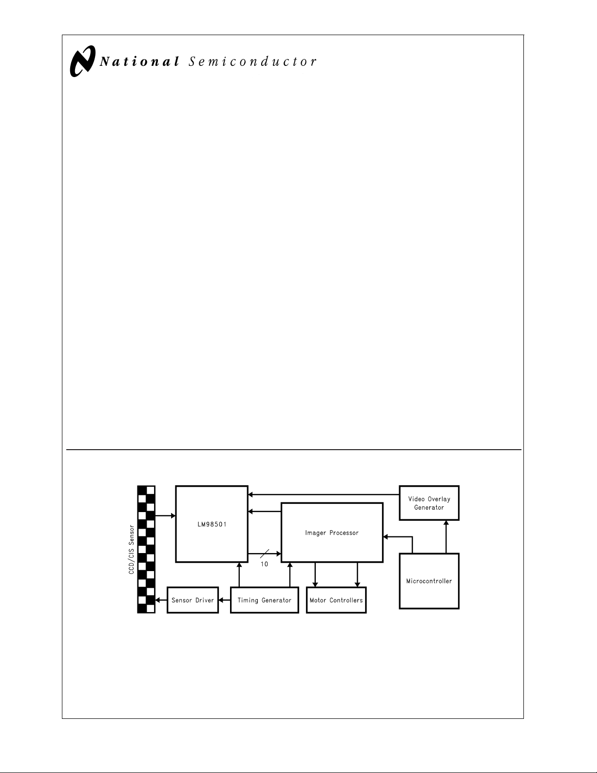
Typical Digital Camera Block Diagram
DS101292-1
© 2000 National Semiconductor Corporation DS101292 www.national.com
Page 2
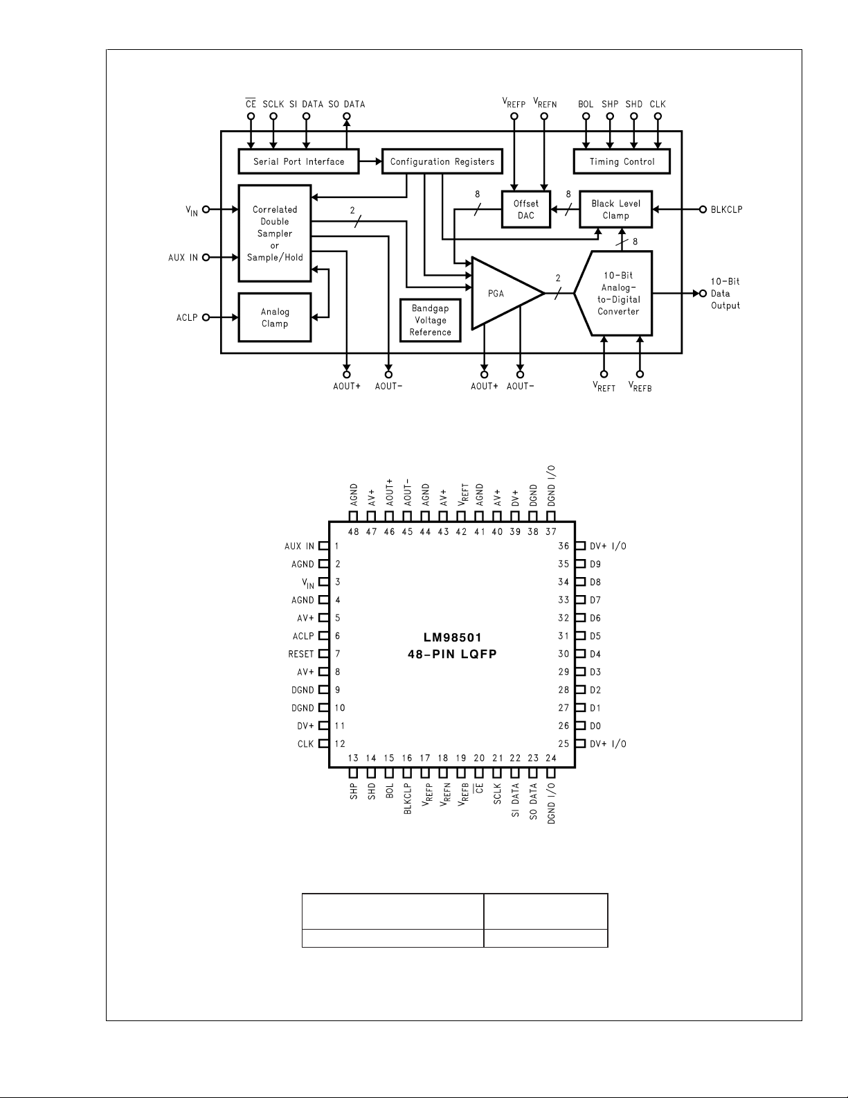
Overall Chip Block Diagram
LM98501
LM98501 Chip Pin Out
DS101292-2
FIGURE 1. Chip Block Diagram
FIGURE 2. Pin Out Diagram
Ordering Information
Commercial
(0˚C ≤ T
LM98501CCVBH LQFP
www.national.com 2
≤ +70˚C)
A
DS101292-3
NS Package
Page 3
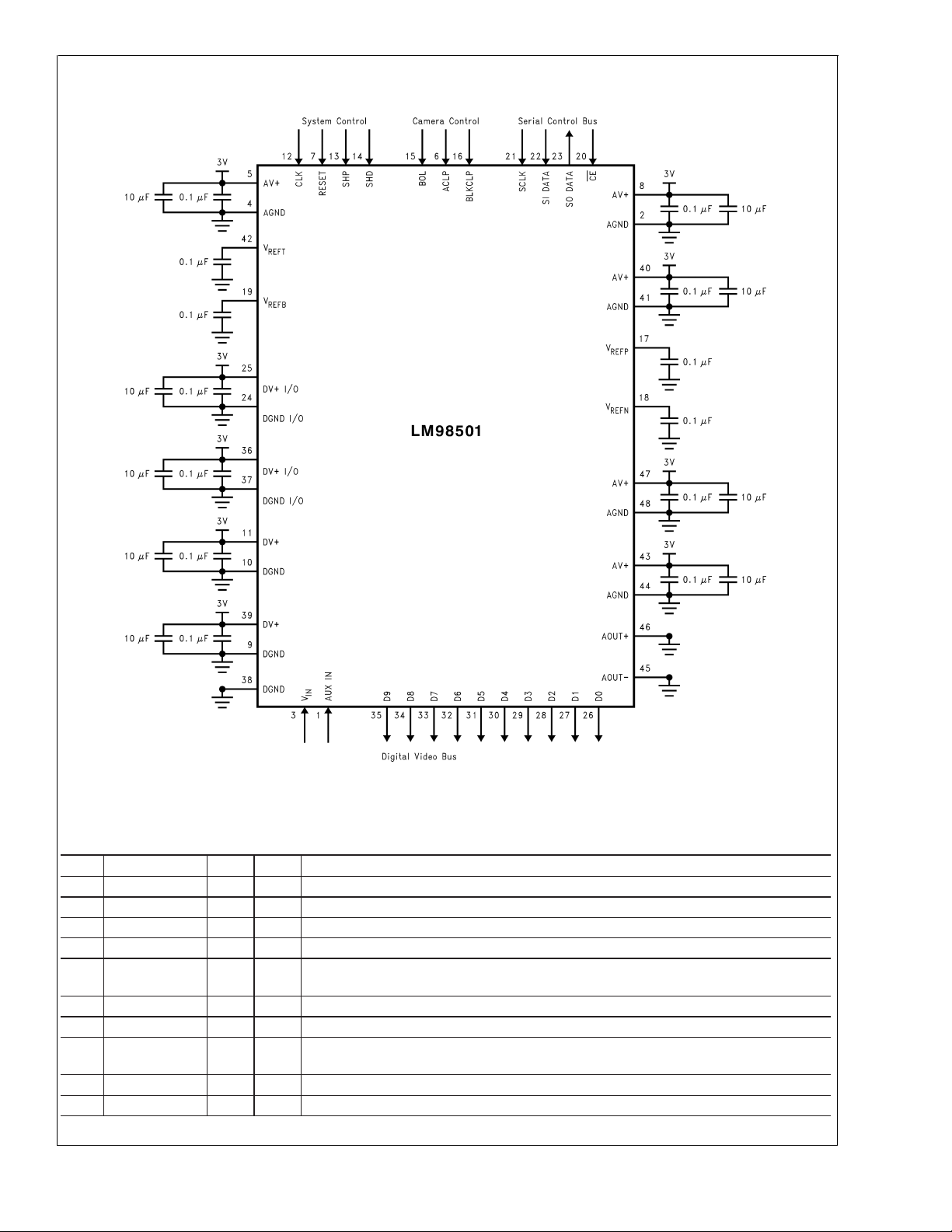
Typical Application Circuit
LM98501
DS101292-4
FIGURE 3. Typical Application Circuit Diagram
Pin Descriptions
Pin Name I/O Typ Description
1 AUX IN I A Auxiliary analog input.
2 AGND P Analog ground return.
3V
4 AGND P Analog ground return.
5 AV+ P +3V power supply for the analog circuits. Bypass each supply pin with 0.1 µF and
6 ACLP I D Analog clamp switch. Float pin when function not being used.
7 RESET I D Active-high master reset. Float pin when function not being used.
8 AV+ P +3V power supply for the analog circuits. Bypass each supply pin with 0.1 µF and
9 DGND P Digital ground return.
10 DGND P Digital ground return.
IN
I A Analog input. AC-couple input signal through a 0.1 µF capacitor
10 µF capacitors in parallel.
10 µF capacitors in parallel.
www.national.com3
Page 4
Pin Descriptions (Continued)
Pin Name I/O Typ Description
LM98501
11 DV+ P +3V power supply for the digital circuits. Bypass each supply pin with 0.1 µF and
10 µF capacitors in parallel.
12 CLK I D 27 MHz clock input.
13 SHP I D Correlated double sampler reset voltage clamp override. Programmable active-high or
active-low through serial interface. Connect to +3V digital supply when function not
being used (register values in default condition).
14 SHD I D Correlated double sampler video signal voltage sample override. Programmable
active-high or active-low through serial interface. Connect to +3V digital supply when
function not being used (register values in default condition).
15 BOL I D Active-high beginning of line switch input. Hold high during entire line of effective
pixels. Hold low during blanking period.
16 BLKCLP I D Active-high black level clamp switch input. Pulse high during black pixels to eliminate
black pixel offset from video signal.
17 V
18 V
19 V
REFP
REFN
REFB
20 CE
21 SCLK I D Serial interface clock used to decode the serial input data.
22 SI DATA I D Serial interface input port.
23 SO DATA O D Serial interface output port.
24 DGND I/O P Digital output driver ground return.
25 DV+ I/O P +3V power supply for the digital output driver circuits. Bypass each supply pin with
26 D0 O D Digital output. Bit 0 of 9 (LSB) of the digital video output bus.
27 D1 O D Digital output. Bit 1 of 9 of the digital video output bus.
28 D2 O D Digital output. Bit 2 of 9 of the digital video output bus.
29 D3 O D Digital output. Bit 3 of 9 of the digital video output bus.
30 D4 O D Digital output. Bit 4 of 9 of the digital video output bus.
31 D5 O D Digital output. Bit 5 of 9 of the digital video output bus.
32 D6 O D Digital output. Bit 6 of 9 of the digital video output bus.
33 D7 O D Digital output. Bit 7 of 9 of the digital video output bus.
34 D8 O D Digital output. Bit 8 of 9 of the digital video output bus.
35 D9 O D Digital output. Bit 9 of 9 (MSB) of the digital video output bus.
36 DV+ I/O P +3V power supply for the digital output driver circuits. Bypass each supply pin with
37 DGND I/O P Digital output driver ground return.
38 DGND P Digital ground return.
39 DV+ P +3V power supply for the digital circuits. Bypass each supply pin with 0.1 µF and 10
40 AV+ P +3V power supply for the analog circuits. Bypass each supply pin with 0.1 µF and 10
41 AGND P Analog ground return.
42 V
REFT
43 AV+ P +3V power supply for the analog circuits. Bypass each supply pin with 0.1 µF and 10
44 AGND P Analog ground return.
45 AOUT− O A Negative differential analog output from correlated double sampler or PGA (selectable
IO A Top of DAC reference ladder. Normally bypassed with a 0.1 µF capacitor. An external
DAC reference voltage may be applied to this pin.
IO A Bottom of DAC reference ladder. Normally bypassed with a 0.1 µF capacitor. An
external DAC reference voltage may be applied to this pin.
IO A Bottom of ADC reference ladder. Normally bypassed with a 0.1 µF capacitor. An
external ADC reference voltage may be applied to this pin.
I D Active-low chip enable for the serial interface.
0.1 µF and 10 µF capacitors in parallel.
0.1 µF and 10 µF capacitors in parallel.
µF capacitors in parallel.
µF capacitors in parallel.
IO A Top of ADC reference ladder. Normally bypassed with a 0.1 µF capacitor. An external
ADC reference voltage may be applied to this pin.
µF capacitors in parallel.
through the serial interface).
www.national.com 4
Page 5

Pin Descriptions (Continued)
Pin Name I/O Typ Description
46 AOUT+ O A Positive differential analog output from correlated double sampler or PGA (selectable
through the serial interface).
47 AV+ P +3V power supply for the analog circuits. Bypass each supply pin with 0.1 µF and 10
µF capacitors in parallel.
48 AGND P Analog ground return.
Legend: (I=Input), (O=Output), (IO=Bi-directional), (P=Power), (D=Digital), (A=Analog).
LM98501
www.national.com5
Page 6
Absolute Maximum Ratings (Notes 1, 2)
If Military/Aerospace specified devices are required,
LM98501
please contact the National Semiconductor Sales Office/
Distributors for availability and specifications.
Any Positive Supply Voltage 4.2V
Voltage on Any Input or Output Pin −0.3V to +4.2V
Input Current at Any Pin (Note 3)
Package Input Current (Note 3)
=
Package Dissipation at T
(Note 4)
25˚C
A
±
35 mA
±
50 mA
ESD Susceptibility (Note 5)
Human Body Model 2000V
Machine Model 200V
Soldering Temperature Infrared,
10 seconds (Note 6) 260˚C
DC and Logic Level Specifications
The following specifications apply for DV+=AV+=DV + I/O=+3.0V, C
noted. Boldface limits apply for T
Symbol Parameter Conditions
DIGITAL INPUT CHARACTERISTICS
V
IH
V
IL
I
IH
I
IL
Logical “1” Input Voltage 2.0 V
Logical “0” Input Voltage 1.0 V
Logical “1” Input Current VIH= DV+, Digital Inputs Except
Logical “0” Input Current VIL= DGND −100 nA
DIGITAL OUTPUT CHARACTERISTICS
V
OH
V
OL
I
OS
Logical “1” Output Voltage DV+ = 3.3V, I
Logical “0” Output Voltage DV+ = 3.3V, I
Output Short Circuit Current 30 mA
POWER SUPPLY CHARACTERISTICS
IA Analog Supply Current P
ID Digital Supply Current P
ID I/O Digital Output Driver Supply
Current
=
to T
T
A
MIN
: all other limits T
MAX
Reset
V
= DV+, Reset (internal
IH
pull-down resistor)
DV+ = 2.7V, I
DV+ = 2.7V, I
= LOW 56.8 mA
D
P
= HIGH 3.1 5.0 mA
D
= LOW 6.5 mA
D
P
= HIGH 0.1 1.0 mA
D
P
= LOW 2.3 mA
D
P
= HIGH 0.1 1.0 mA
D
Storage Temperature −65˚C to +150˚C
Operating Ratings (Notes 1, 2)
Operating Temperature Range 0˚C ≤ T
All Supply Voltages +2.7V to +3.3V
Voltage Range 0.0V to AV+
V
IN
Voltage Range 2.0V to 2.5V
V
REFT
Voltage Range 0.4V to 0.9V
V
REFB
Voltage Range 1.3V to 1.9V
V
REFP
Voltage Range 1.3V to 1.9V
V
REFN
All Digital Inputs Voltage Range −0.05V to +3.35V
=
10 pF, and f
L
=
25˚C (Note 7).
A
= −0.5 mA 2.5
OUT
= −0.5 mA 2.3
OUT
= 1.6 mA 0.4
OUT
= 1.6 mA 0.4
OUT
=
27 MHz unless otherwise
CLK
Min
(Note 9)
Typical
(Note 8)
100 nA
400 µA
Max
(Note 9)
≤ +70˚C
A
Units
V
V
Power Dissipation Specifications
The following specifications apply for DV+=AV+=DV + I/O=+3.0V, C
noted. Boldface limits apply for T
=
to T
T
A
MIN
: all other limits T
MAX
=
10 pF, and f
L
=
25˚C (Note 7).
A
Symbol Parameter Conditions
PWR Average Power Dissipation AV+=DV+=DV+ I/O=2.7V 150
AV+=DV+=DV+ I/O=3.3V 240
www.national.com 6
=
27 MHz unless otherwise
CLK
Min
(Note 9)
(Note 8)
Typical
Max
(Note 9)
Units
mWAV+=DV+=DV+ I/O=3.0V 195
Page 7
Correlated Double Sampler Specifications
The following specifications apply for DV+=AV+=DV + I/O=+3.0V, C
noted. Boldface limits apply for T
Symbol Parameter Conditions
V
IN
I
IN
C
IN
R
IN
t
AD
t
SHP
Input Voltage Level 1.0 V
Input Leakage Current 010nA
Input Capacitance 5pF
Input Resistance 10 kΩ
Aperture Delay 2ns
CLK Falling Edge to SHP Falling
Edge
t
SHD
CLK Rising Edge to SHD Falling
Edge
=
to T
T
A
MIN
: all other limits T
MAX
PGA Specifications
The following specifications apply for DV+=AV+=DV + I/O=+3.0V, C
noted. Boldface limits apply for T
Symbol Parameter Conditions
Gain Resolution 8 Bits
Step Size (Gain / Resolution) 0 0.125 dB
Maximum Gain 32.0 dB
Minimum Gain 0.0 dB
Gain Error
Gain Error
@
20 MHz Deviation from Best-Fit Line after
@
27 MHz Deviation from Best-Fit Line after
=
to T
T
A
MIN
: all other limits T
MAX
End-Point Correction
End-Point Correction
=
10 pF, and f
L
=
25˚C (Note 7).
A
=
10 pF, and f
L
=
25˚C (Note 7).
A
=
27 MHz unless otherwise
CLK
Min
(Note 9)
Typical
(Note 8)
10
14
=
27 MHz unless otherwise
CLK
Min
(Note 9)
Typical
(Note 8)
±
±
LM98501
Max
(Note 9)
Max
(Note 9)
5
5
Units
p-p
Units
%
%
Offset DAC and Black Level Clamp Specifications
The following specifications apply for DV+=AV+=DV + I/O=+3.0V, C
noted. Boldface limits apply for T
=
to T
T
A
MIN
: all other limits T
MAX
Symbol Parameter Conditions
R
REF
Reference Ladder Resistance 50 kΩ
Resolution
Offset Adjustment Range PGA Gain=1.0 dB
Black Level Clamp Accuracy PGA Gain=0.0 dB
PGA Gain=32.0 dB
t
BLKCLP
Black Clamp Switch Pulse Width 20 T
=
10 pF, and f
L
=
25˚C (Note 7).
A
Analog to Digital Converter Specifications
The following specifications apply for DV+=AV+=DV + I/O=+3.0V, C
noted. Boldface limits apply for T
=
to T
T
A
MIN
: all other limits T
MAX
Symbol Parameter Conditions
R
V
V
V
V
REF
REFT
REFB
REFT
REFB
Reference Ladder Resistance 850 1000 1150 kΩ
Top of Reference Ladder V
Bottom of Reference Ladder V
–
Differential Reference Voltage V
not driven externally 2.25 2.4 V
REFT
not driven externally 0.6 0.75 V
REFB
and V
REFT
REFB
externally
Overrange Output Code V
Underrange Output Code V
>
V
IN
REFT
<
V
IN
REFB
Guaranteed No Missing Codes 10 Bits
=
L
=
25˚C (Note 7).
A
not driven
10 pF, and f
=
27 MHz unless otherwise
CLK
Min
(Note 9)
Typical
(Note 8)
±
±
93 mV
±
0.5 LSB
±
0.5 LSB
=
27 MHz unless otherwise
CLK
Min
(Note 9)
Typical
(Note 8)
1.5 V
1023
0
Max
(Note 9)
Units
7 Bits
CLK
Max
(Note 9)
Units
www.national.com7
Page 8
AC Electrical Characteristics
The following specifications apply for DV+=AV+=DV + I/O=+3.0V, C
Boldface limits apply for T
LM98501
=
to T
T
A
MIN
: all other limits T
MAX
Symbol Parameter Conditions
f
CLK
T
CLK
t
ch
t
cl
t
rc,tfc
Input Clock Frequency 1 27 30 MHz
Input Clock Period 33 37 1000 ns
Clock High Time
Clock Low Time
Clock Duty Cycle
@
CLK
max
@
CLK
max
@
CLK
max
Clock Input Rise and Fall Time 5 ns
Pipeline Delay (Latency) 7 T
t
VALID
t
OH
t
OD
Data Valid Time 27 ns
Output Data Hold Time 9 13 19 ns
Output Delay Time 14 20 26 ns
=
25˚C (Note 7).
A
=
10 pF, and f
L
(Note 9)
=
27 MHz unless otherwise noted.
CLK
Min
Typical
(Note 8)
Max
(Note 9)
15 ns
15 ns
45/55 min/max
Full Channel Performance Specifications
The following specifications apply for DV+=AV+=DV + I/O=+3.0V, C
noted. Boldface limits apply for T
=
to T
T
A
MIN
: all other limits T
MAX
=
10 pF, and f
L
=
25˚C (Note 7).
A
Symbol Parameter Conditions
DNL Differential Non-Linearity −1.0
INL Integral Non-Linearity +3.0/−1.5 LSB
=
*
SNR 0 dB Gain, 1.0V Input
ENOB Effective Number of Bits
THD Total Harmonic Distortion
*
20 log10(VIN/RMS Output Noise)
Note 1: Absolute Maximum Ratings indicate limits beyond which damage to the device may occur. Operating Ratings indicate conditions for which the device is functional, but do not guarantee specific performance limits. For guaranteed specifications and test conditions, see the Electrical Characteristics. The guaranteed specifications apply only for the test conditions listed. Some performance characteristics may degrade when the device is not operated under the listed test conditions.
Note 2: All voltages are measured with respect to GND=AGND=DGND=0V, unless otherwise specified.
Note 3: When the voltage at any pin exceeds the power supplies (V
maximum package input current rating limits the number of pins that can safely exceed the power supplies with in input current of 25 mA to two.
Note 4: The absolute maximum junction temperature (T
junction-to-ambient thermal resistance (
*
JAis 69˚C/W, so P
LQFP,
device under normal operation will typically be about 180 mW. The values for maximum power dissipation listed above will be reached only when the LM98501 is
operated in a severe fault condition.
Note 5: Human body model is 100 pF capacitor discharged through a 1.5 kΩ resistor. Machine model is 220 pF discharged through 0Ω.
Note 6: See AN450, “Surface Mounting Methods and Their Effect on Product Reliability”, or the section entitled “Surface Mount” found in any post 1986 National
Semiconductor Linear Data Book, for other methods of soldering surface mount devices.
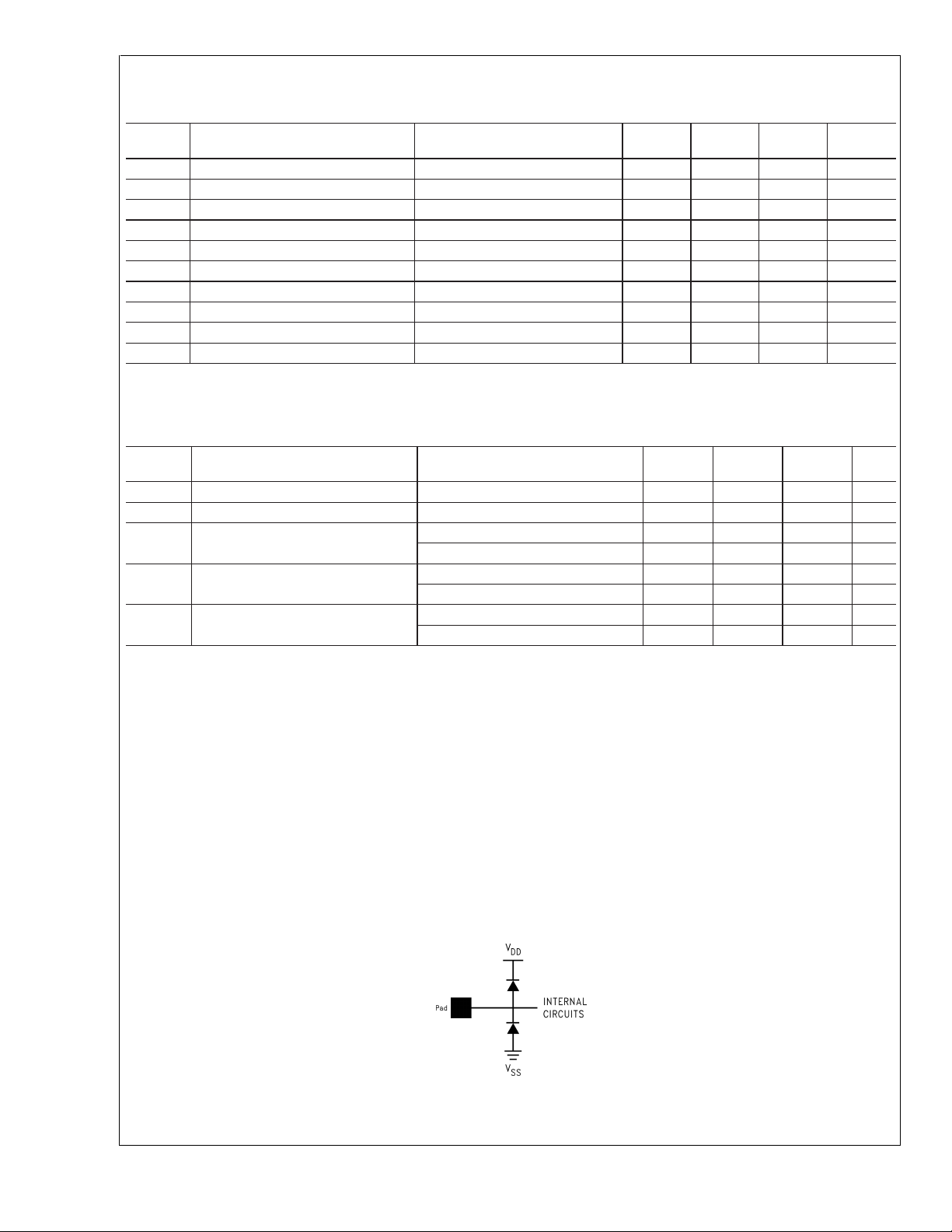
Note 7: The analog inputs are protected as shown below. Input voltage magnitude up to 500 mV beyond the supply rails will not damage this device. However, input
errors will be generated if the input goes above AV+ and below AGND.
DMAX
*
JA), and the ambient temperature (TA), and can be calculated using the formula P
=
1,811mW at 25˚C and 1,159 mW at the maximum operating ambient temperature of 70˚C. Note that the power dissipation of this
@
f
27 MHz 60 dB
CLK
=
@
f
20 MHz 61 dB
CLK
=
@
f
27 MHz 7.5 Bits
CLK
=
@
f
20 MHz 7.6 Bits
CLK
=
@
f
27 MHz −51 dB
CLK
=
@
f
20 MHz −60 dB
CLK
<
GND or V
IN
) for this device is 150˚C. The maximum allowable power dissipation is dictated by T
JMAX
>
AV+ or DV+), the current at that pin should be limited to 25 mA. The 50 mA
IN
=
27 MHz unless otherwise
CLK
Min
(Note 9)
Typical
(Note 8)
±
0.5 1.5 LSB
=
(T
DMAX
JMAX–TA
Max
(Note 9)
)/*JA. In the 48-pin
JMAX
Units
CLK
Units
, the
Note 8: Typical figures are at T
Note 9: Test limits are guaranteed to National’s AOQL (Averaging Outgoing Quality Level).
www.national.com 8
=
25˚C, and represent most likely parametric norms.
J
DS101292-18
Page 9

Typical Performance Characteristics
LM98501
DNL vs. Temperature
DNL vs. Clock Frequency
DS101292-19
DNL vs. Supply Voltage
DS101292-20
DNL vs. Clock Duty Supply
INL vs. Temperature
DS101292-21
DS101292-23
DS101292-22
INL vs. Supply Voltage
DS101292-24
www.national.com9
Page 10

Typical Performance Characteristics (Continued)
LM98501
INL vs. Clock Frequency
INL vs. Clock Duty Cycle
DS101292-25
Power Dissipation vs. Temperature
DS101292-27
Actual vs. Ideal PGA Gain and Clock Frequency
DS101292-26
Power Dissipation vs. Clock Frequency
DS101292-28
PGA Gain vs. Supply Voltage and Clock Frequency
DS101292-29
www.national.com 10
DS101292-30
Page 11

Typical Performance Characteristics (Continued)
LM98501
Grounded Input Noise
@
20 MHz Clock Frequency
DS101292-31
Spectral Response@20 MHz Clock Frequency
Grounded Input Noise@27 MHz Clock Frequency
DS101292-32
Spectral Response@27 MHz Clock Frequency
DS101292-33
DNL vs. Power Setting@27 MHz Clock Frequency
DS101292-35
DS101292-34
Power Dissipation vs. Power Setting
DS101292-36
www.national.com11
Page 12

CDS Sampling Timing
LM98501
1
SHP overrides the CLAMP signal’s falling edge for sampling the reset voltage (SHP is active-low by default).
2
The CLAMP signal is an internal signal derived from the CLK input whose falling edge samples the CCD reset voltage by default.
FIGURE 4. Pixel Rate Reset Voltage Sampling
1
SHP overrides the CLAMP signal’s falling edge for sampling the reset voltage (SHD is active-low by default).
2
The SAMPLE signal is an internal signal derived from the CLK input whose falling edge samples the CCD video signal by default.
FIGURE 5. Pixel Rate Video Signal Sampling
Horizontal Interval Timing
DS101292-5
DS101292-6
FIGURE 6. Typical Horizontal Interval Timing
www.national.com 12
DS101292-7
Page 13

Digital Output Timing
System Timing
LM98501
DS101292-8
FIGURE 7. Digital Output Data Timing
FIGURE 8. System Timing
System Overview
INTRODUCTION
The LM98501 is a 10-bit, complete analog-to-digital camera
signal processor for use with CCD imager systems operating
from a single +3V supply. The internal processing is carefully
optimized to maintain the signal-to-noise ratio and excellent
dynamic performance of most popular CCD imagers. The
system block diagram of the LM98501, shown on the cover
page of the datasheet, highlights the main features of the device: correlated double sampling (CDS), 0 dB–32 dB digitally
programmable gain amplifier (PGA), digital black level correction feedback loop, 8-bit DAC, analog clamp, bandgap
voltage reference, and a 10-bit, 27 MHz analog-to-digital
converter.
DS101292-9
CORRELATED DOUBLE SAMPLING
Correlated double sampling (CDS) is a key feature in CCD
image processors. The sampling process consists of two
samples being taken for each pixel. The first stores the reset
voltage of the input pixel, and the second stores the video
signal amplitude. The two samples are subtracted from one
another, effectively removing the reset error offset of each
pixel. This sampling system operates at 27 MHz, allowing
the use of imagers that have resolution at high speeds. Operation at these higher clock rates generates electronic images similar to a high-speed camera, preventing blearing of
the image caused by motion during the exposure.
www.national.com13
Page 14

System Overview (Continued)
LM98501
FIGURE 9. Correlated Double Sampling
PROGRAMMABLE GAIN AMPLIFIER
In a CCD imager, there may be millions of photo diodes that
normally have some gain variation from pixel to pixel. Other
gain errors are generated by the amount of light transmission and the quality of the color filters on the front of each
pixel of the imager. These filters make it possible for camera
to recognize color; therefore, each filter has to have correct
gain in order to generate the electronic voltages that would
be equal to white. Luminosity of a scene may have a colorcast, and the gain of a pixel must be changed in order to
compensate for the colorcast. These three sources of gain
error associated with each pixel are compensated for with a
wide bandwidth programmable gain amplifier that operates
at a pixel rate. The amplifier has a gain ranging from
0 dB–32 dB, and is “linear in dB” as shown in
linear in dB amplifier contains more gain steps in the lower
portion of the gain range so that color balance may be maintained during low light levels.
AUXILIARY INPUT
The LM98501 includes a high-level video switch that allows
a recorder playback video signal to be selected instead of
the camera image. This feature is especially useful when
adding electronic titles to images in the digital domain. In addition, the PGA gain and DAC offset are set to register 0 in
DS101292-10
Figure 16
.A
each case; therefore, appropriate gain and offset values
should be written to PGA gain and DAC offset register 0 prior
AUX IN usage.
BLACK LEVEL CLAMP
CCD signal processors require a reference level for the
proper handling of input signals; this reference level is commonly referred to as the black level. The LM98501 is designed to determine a signal’s black level during the CCD imager’s optical black pixels.
The LM98501 provides both an analog clamp and a digital
black level correction loop. Pulsing the ACLP pin during optical black pixels causes the analog clamp circuitry to remove the offset associated with the input signal. During
dummy black pixels at the end of a horizontal line, setting the
BLKCLP pin for a minimum of 20 CLK cycles enables the
digital black level correction loop.
Actual black level correction may be performed through one
of two available methods— automatic or manual. In automatic mode, the black level is sampled from the ADC output
during black pixels by setting the BLKCLP input of the
LM98501. The ADC black level output value is then averaged over eight pixels and subtracted from the desired black
level stored in the black level configuration register. The result of the subtraction may then be integrated by a preset
scaling factor, effectively smoothing any sharp transitions
present in the black level signal, before the resulting error is
finally applied to the input of the PGA as an analog offset
generated by the DAC. The offset integration scaling factor is
stored in two bits of the software control register 0, and the
values available range from the full offset to offset
divided-by-16. In addition, an offset output enable bit is provided in the software control register 0, which when set,
routes the offset value to the digital output bus rather than
the DAC. Use of the automatic mode involves enabling the
black level offset auto-calibration bit in the software control
register 0 through the serial interface.
The manual method is intended for use with processing systems where the desired black level correction loop is external to the LM98501. In this mode, up to four available configuration registers may be used to store predetermined
offset values that will be applied on a pixel-rate basis. During
the vertical interval, new values may be stored in these registers for each horizontal line.
FIGURE 10. Digital Black Level Correction Loop
www.national.com 14
DS101292-11
Page 15

System Overview (Continued)
ANALOG CLAMP
During optical black pixels, an offset often appears on the
CCD generated input signal. This offset may be seen by the
CDS circuitry as a valid video signal rather than the actual
black level signal; therefore, the LM98501 provides an analog clamp designed to eliminate this offset during black pixels. Pulsing the analog input pin, ACLP, causes the output of
the CDS to be sampled by the analog clamp circuitry. Subsequently, an adjustment is made to the CDS reference voltages by the analog clamp to effectively eliminate any offset
present in the signal during black pixels.
10-BIT ANALOG-TO-DIGITAL CONVERTER
The selected imager’s analog signal is sampled by the CDS
and amplified to match the input requirements of the 10-bit
analog-to-digital converter by the PGA. The final step performed by the system is to convert the selected analog image to digital values with a 10 bits of resolution. The ADC
has differential inputs and outputs (internally) which aids in
the coping with headroom constraints common to +3V systems. Data is acquired at the falling edge of the clock and is
available at the digital output pins 7.0 clock cycles plus t
later.
INTERNAL VOLTAGE REFERENCE
An on-board, temperature stable voltage reference is employed based on a differential, continuous-time bandgap circuit. The employment of this on-chip reference eliminates
the need for external reference drive circuitry and components, minimizing cost and board space in a design. The use
of external bypass capacitors from the reference pins to
ground is recommended for reducing reference drive requirements, resulting in reduced power dissipation. A second
on-chip reference is used exclusively for the offset DAC and
follows the same procedures for bypassing with external capacitors.
INTERNAL TIMING GENERATION
All if the necessary clocks for the CDS and ADC operation
are generated internally from the LM98501’s master clock input. The CDS sampling clocks may be overridden by the
user via the SHP and SHD clock inputs. As depicted in
ure 4
and
Figure 5
, there are two signals generated internally
for CDS sampling referred to as CLAMP and SAMPLE.
These signals provide the rising edge reference for the sampling of the CCD input signal. The timing of CLAMP and
SAMPLE is derived from the clock; therefore, shifting the
clock phasing with respect to the CCD input signal would
also shift the rising (and falling) edges of CLAMP and
SAMPLE. The actual sampling of the CCD’s reset voltage
and video signal is performed on the falling edges of the
CLAMP and SAMPLE signals respectively. The user may
modify the position of the falling edges where the sampling
of the CCD input occurs by driving the SHP and SHD inputs
of the LM98501. The falling edges of SHP and SHD will supersede the falling edges of CLAMP and SAMPLE respectively and cause the duration of the sample pulse to shorten
accordingly. As evidenced in
Figure 4
and
Figure 5
ing edges of SHP and SHD should not occur earlier than
t
SHP
or t
after the respective falling [SHP] (or rising
SHD
[SHD]) edge of CLK.
OD
Fig-
, the fall-
SERIAL INTERFACE AND CONFIGURATION
REGISTERS
There are many options available to the user that may be
programmed via the LM98501’s serial interface. Configuration values are stored in registers for use by several functions such as programmable gain, offset, black level, and
color filter array.
The LM98501’s serial interface is used to store values into
16 8-bit configuration registers. Upon power-up or external
reset, the configuration registers will contain their respective
default values. Default values place the LM98501 in ‘single
channel’ mode, where only one PGA gain and offset are applied to the input signal.
The master CLK input is required to be running during serial
interface commands. Each command issued through the serial interface must have a minimum of 13 data bits (see
ures 13, 14
).
Fig-
PGA GAIN
The four PGA gain registers store four possible gain values
for the programmable gain amplifier (PGA). For example,
these four gain values may correspond to four possible colors in a color filter array.
ANALOG OFFSET
The analog offset registers store four possible values that
correspond to the four gain values. For example, the value
stored in the PGA gain register 0 (address 0h) is used in conjunction with the offset value stored in the analog offset register 0 (address 4h). This allows for four possible combinations of PGA gain and analog offset, one for each color filter.
These registers are read-only when offset auto-calibration is
enabled in the software control register 0. It should be noted
that each offset DAC step (1 LSB) corresponds to a 0.4 LSB
step at the ADC output. Therefore, if an offset of 20 digital
codes is desired at theADC output, a digital code value of 50
should be stored in the analog offset register(s). As a result,
the maximum offset seen at the ADC output as a result of
digital code values stored in the analog offset register(s) is
±
54 codes. It is possible to increase the digital output range
of the analog offset DAC, resulting in a increased maximum
ADC output code corresponding to a given DAC input. for
more information on increasing the DAC range, please see
ANALOG OFFSET DAC RANGE ADJUSTMENT
.
OUTPUT BLACK LEVEL
The output black level register is occupied by an 8-bit word
stored by the user that specifies the output level corresponding to optical black. For example, a user that wants an output
level of 16 for black pixels must write this value into the register during the horizontal interval. Once this has been accomplished, driving the BLKCLP high for 20 cycles of CLK
activates the digital black clamp loop and the black level is
forced to the value stored in the output black level register, in
the example case the code value of 16. As a result of the relationship between the DAC input and the ADC output (see
’Analog Offset’), the largest output black level code the
LM98501 is capable of clamping to is 54 codes.
LM98501
www.national.com15
Page 16

System Overview (Continued)
LM98501
DS101292-37
FIGURE 11. ADC Output vs. Black Level Register Value
COLOR FILTER ARRAY (CFA) CONFIGURATION
In order to utilize the LM98501’s programmable pixel-rate
gain, a color filter array (CFA)pattern must be defined. Some
commonly used CFApatterns are as follows:
Bayer Pattern
Line 0 Green Red Green Red
Line 1 Blue Green Blue Green
CMYG Pattern
Line 0 Cyan Magenta Yellow Green
Line 1 Cyan Green Yellow Magenta
Therefore, two 8-bit words must be written to the CFA line
registers to specify the CFA pattern being used. Also, two
2-bit numbers must be written to the CFA definition register
indicating the number of pixels per pattern in each line of the
defined CFA pattern. The information contained in the CFA
line registers indicates the registers where the respective
PGA gain and offset values are stored. For example, a system using the Bayer pattern defined above would first write
four PGA gains and their respective offsets into the four PGA
gain and four analog offset registers. Next, two 8-bit words
(one word/CFA line) would be written to the CFA configuration registers. The 8-bit CFA configuration words each consist of four 2-bit numbers, each of which is the address for
the gain and offset values of the color that appears in that location in the CFA line. Finally, two 2-bit numbers specifying
the number of elements in each CFAline must be written into
the CFAdefinition register. A CFAconfiguration will then contain four 2-bit numbers indicating the registers where the
gain and offset values are located for a maximum of four colors on each CFA line. In addition, the CFA definition register
will contain two 2-bit numbers that designate the number of
elements used in each CFA line for the particular CFA pattern being applied to the system.
Example A contains a CFA pattern that repeats the colors
cyan and magenta on the first line, and repeats the pattern
blue, green, green, blue on the second line. Each 2-bit number in the CFA line registers refers to a common set of PGA
gain and offset registers for each color. The first line indi-
cates that the color magenta uses the gain and offset values
stored in PGA gain register 1 (address 1h) and analog offset
register 1 (address 5h). Also, the first line indicates that the
color cyan uses the gain and offset values in PGA gain register 2 (address 2h) and analog offset register 2 (address
6h). The second line indicates gain and offset values for the
color blue and the color green in the same fashion as the first
line.
Example A
70
CFA Line 0 XX XX 01 10
CFA Line 1 11 00 00 11
CFA Definition 00 00 11 01
In addition to specifying the gain and offset for each line, it is
also necessary to specify the number of elements contained
in each CFAline’s pixel pattern. The CFAdefinition register is
used to store this value (number of elements per line). In example A, the user has stored the 2-bit binary number 01 into
the CFA definition register’s two LSB’s indicating that the
pattern in line 0 contains two repeating colors or elements.
Also, the 2-bit binary number 11 has been written into bit 2
and bit 3 of the CFAdefinition register indicating that the respective CFA pattern contains four repeating colors or elements, as the colors blue and green alternate position in the
example pattern.
Once both lines for the pattern have been stored, it is applied
when the beginning of line (BOL) signal is asserted by the
user. One line of the CFA pattern is applied repeatedly until
the BOL signal is reset (at the end of the current line). Once
the BOL signal is set again, the CFA line information is
changed from that defined by the CFAline 0 register to that
defined by the CFA line 1 register and the process starts
again. For more details of the timing of the BOL signal,
please refer to
SOFTWARE CONTROL
There are two software control registers accessible via the
serial interface. The software control registers are divided
into customer (register 0) and advanced (register 1) functions. Please refer to the register data descriptions for more
information on the software control registers.
POWER LEVEL CONTROL
The LM98501 is equipped with two power trim registers that
may be used to adjust power levels of various circuits internal to the device. In its default condition, the LM98501 is set
for optimum power and performance, and modifying the values stored in the power level control registers will affect performance as a result of the change in power level(s). In applications where maximum performance is desired, the
default values should be used. Otherwise, power levels may
be decreased at the slight expense of performance. Please
refer to the register data descriptions for more information
regarding the power level control registers.
TheADC coarse and fine bank power adjustment bits are located in the power level control 2 register, bits 7:4. Altering
these bits may significantly affect performance and power
dissipation. Please see “DNL vs. Power Control Setting
27 MHz Clock Frequency” and “Power Dissipation vs. Power
Control Setting” on page 11.
Figure 6
.
@
www.national.com 16
Page 17

Register Memory Map
Title Address Default Value
PGA Gain 0 0000 0000 0000 (0d)
PGA Gain 1 0001 0000 0000 (0d)
PGA Gain 2 0010 0000 0000 (0d)
PGA Gain 3 0011 0000 0000 (0d)
Analog Offset 0 0100 0000 0000 (0d)
Analog Offset 1 0101 0000 0000 (0d)
Analog Offset 2 0110 0000 0000 (0d)
Analog Offset 3 0111 0000 0000 (0d)
CFA Configuration 0 1000 0000 0000 (0d)
CFA Configuration 1 1001 0000 0000 (0d)
CFA Definition 1010 XXXX 0000 (0d)
Output Black Level 1011 0001 0000 (32d)
Software Control 0 1100 0100 1110 (78d)
Software Control 1 1101 XX00 0X00 (0d)
Power Level Control 0 1110 1010 1010 (170d)
Power Level Control 1 1111 0101 1010 (90d)
FIGURE 12. Register Memory Map
Register Data
The following section describes all available registers in the
LM98501 register bank and their functions.
PGA GAIN REGISTERS
Register Name PGA Gain 0
Address 0 Hex
Type Read/Write
Reset Value 0000 0000 Binary
Bit Bit Symbol Description
[7:0] PGA Gain 0.0 dB–32.0 dB in 0.125 dB
steps.
Register Name PGA Gain 1
Address 1 Hex
Type Read/Write
Reset Value 0000 0000 Binary
Bit Bit Symbol Description
[7:0] PGA Gain 0.0 dB–32.0 dB in 0.125 dB
steps.
Register Name PGA Gain 2
Address 2 Hex
Type Read/Write
Reset Value 0000 0000 Binary
Bit Bit Symbol Description
[7:0] PGA Gain 0.0 dB–32.0 dB in 0.125 dB
steps.
Reset Value 0000 0000 Binary
Bit Bit Symbol Description
[7:0] PGA Gain 0.0 dB–32.0 dB in 0.125 dB
steps.
ANALOG OFFSET REGISTERS
Register Name Analog Offset 0
Address 4 Hex
Type Read/Write
Reset Value 0000 0000 Binary
Bit Bit Symbol Description
[7:0] Signed Analog
Offset
Register Name Analog Offset 1
Address 5 Hex
Type Read/Write
Reset Value 0000 0000 Binary
Bit Bit Symbol Description
[7:0] Signed Analog
Offset
Register Name Analog Offset 2
Address 6 Hex
Type Read/Write
Reset Value 0000 0000 Binary
Digital representation of the
analog offset to be applied to
the input of the PGA. See
“Analog Offset” on page 15.
Digital representation of the
analog offset to be applied to
the input of the PGA. See
“Analog Offset” on page 15.
LM98501
Register Name PGA Gain 3
Address 3 Hex
Type Read/Write
www.national.com17
Page 18

Register Data (Continued)
LM98501
Bit Bit Symbol Description
[7:0] Signed Analog
Offset
Register Name Analog Offset 3
Address 7 Hex
Type Read/Write
Reset Value 0000 0000 Binary
Bit Bit Symbol Description
[7:0] Signed Analog
Offset
COLOR FILTER ARRAY REGISTERS
Register Name Color Filter Array Configuration 0
Address 8 Hex
Type Read/Write
Reset Value 0000 0000 Binary
Bit Bit Symbol Description
[7:6] Line0:Pixel3
Gain/Offset
[5:4] Line0:Pixel2
Gain/Offset
[3:2] Line0:Pixel1
Gain/Offset
[1:0] Line0:Pixel0
Gain/Offset
Register Name Color Filter Array Configuration 1
Address 9 Hex
Type Read/Write
Reset Value 0000 0000 Binary
Bit Bit Symbol Description
[7:6] Line1:Pixel3
Gain/Offset
[5:4] Line1:Pixel2
Gain/Offset
Digital representation of the
analog offset to be applied to
the input of the PGA. See
“Analog Offset” on page 15.
Digital representation of the
analog offset to be applied to
the input of the PGA. See
“Analog Offset” on page 15.
2 LSB’s of register
addresses where the gain
and offset for pixel 3 of the
CFA pattern are stored.
2 LSB’s of register
addresses where the gain
and offset for pixel 2 of the
CFA pattern are stored.
2 LSB’s of register
addresses where the gain
and offset for pixel 1 of the
CFA pattern are stored.
2 LSB’s of register
addresses where the gain
and offset for pixel 0 of the
CFA pattern are stored.
2 LSB’s of register
addresses where the gain
and offset for pixel 3 of the
CFA pattern are stored.
2 LSB’s of register
addresses where the gain
and offset for pixel 2 of the
CFA pattern are stored.
Bit Bit Symbol Description
[3:2] Line1:Pixel1
Gain/Offset
[1:0] Line1:Pixel0
Gain/Offset
Register Name Color Filter Array Definition
Address A Hex
Type Read/Write
Reset Value XXXX 0000 Binary
Bit Bit Symbol Description
[3:2] Line 1 Pixels Number of pixels in CFA
[2:1] Line 0 Pixels Number of pixels in CFA
OUTPUT BLACK LEVEL REGISTER
Register Name Output Black Level
Address B Hex
Type Read/Write
Reset Value 0001 0000 Binary
Bit Bit Symbol Description
[7:0] Black Level 0–256 output black level
SOFTWARE CONTROL REGISTERS
Register Name Software Control 0 (Customer)
Address C Hex
Type Read/Write
Reset Value 0100 1110 Binary
Bit Bit Symbol Description
[7] Offset Output
Enable
[6] Serial Output
Enable
[5:4] Offset
Integration
2 LSB’s of register
addresses where the gain
and offset for pixel 1 of the
CFA pattern are stored.
2 LSB’s of register
addresses where the gain
and offset for pixel 0 of the
CFA pattern are stored.
pattern defined in CFA line
1.
pattern defined in CFA line
0.
digital code value. (see
“Output Black Level” on
page 15)
Directs the offset error
calculated by the digital
black level correction loop to
the 10 digital output data
pins.
Enables the serial interface
output for reading register
values.
Offset integration factor
selection:
00 No Scaling
01 Divide-by-4
10 Divide-by-8
11 Divide-by-16
www.national.com 18
Page 19

Register Data (Continued)
Bit Bit Symbol Description
[3] Offset
Auto-Calibration
Enable
[2] SHP/SHD
Active-HIGH
Enable
[1] CDS Enable
(AUX-In
Disable)
[0] Analog Power
Down
Register Name Software Control 1 (Customer)
Address D Hex
Type Read/Write
Reset Value XX00 0X00 Binary
Bit Bit Symbol Description
[5:4] Analog Output
Select
[3] Analog Output
Enable
[1] ADC Reference
Select
[0] DAC Reference
Select
Enables the digital black
level correction loop.
offset registers are read-only
when offset auto-calibration
is enabled.
Inverts the SHP and SHD
inputs causing the CDS to
sample on the rising edges
of SHP and SHD.
Sampling
is performed on the falling
edges of SHP and SHD
when the signals are
Active-low.
Instructs the CDS to sample
the CCD input.
Otherwise,
the AUX In input is sampled
in sample-and-hold mode.
Cuts power to the on-chip
analog circuitry including the
CDS, PGA, ADC, and
bandgap references.
Routes the selected internal
analog signal to the
differential analog output
pins AOUT+ and AOUT−.
00 CDS
01 PGA Stage 1
10 PGA Stage 2
11 PGA Stage 3
Enables the differential
analog output pins AOUT+
and AOUT−. If the analog
outputs are disabled, the
pins should not be loaded.
Reference biasing selection
for the analog-to-digital
converter.
0 Passive Biasing
(Resistors)
1 Active Biasing
(Bandgap)
Reference biasing selection
for the digital-to-analog
converter.
0 Active Biasing
(Bandgap)
1 Passive Biasing
(Resistors)
Analog
Register Name Power Level Control 0
Address E Hex
Type Read/Write
Reset Value 1010 1010 Binary
Bit Bit Symbol Description
[7:6] PGA Stage 1
Amplifier Bias
[5:4] PGA
Common-Mode
Input Bias
[3:2] CDS Amplifier
Bias
[1:0] CDS
Common-Mode
Input Bias
Register Name Power Level Control 1
Address F Hex
Type Read/Write
Reset Value 0101 1010 Binary
Bit Bit Symbol Description
[7:6] ADC Coarse
Bank Bias
[5:4] ADC Fine Bank
Bias
[3:2] PGA Stage 3
Amplifier Bias
[1:0] PGA Stage 2
Amplifier Bias
Adjusts the power level of
the PGA stage 1 amplifier.
The power level is relative to
the value of the binary
number stored.
Adjusts the power level of
the PGA common-mode
input. The power level is
relative to the value of the
binary number stored.
Adjusts the power level of
the CDS amplifier. The
power level is relative to the
value of the binary number
stored.
Adjusts the power level of
the CDS common-mode
input. The power level is
relative to the value of the
binary number stored.
Adjusts the power level of
the ADC coarse bank. The
power level is relative to the
value of the binary number
stored.
Adjusts the power level of
the ADC fine bank. The
power level is relative to the
value of the binary number
stored.
Adjusts the power level of
the PGA stage 3 amplifier.
The power level is relative to
the value of the binary
number stored.
Adjusts the power level of
the PGA stage 2 amplifier.
The power level is relative to
the value of the binary
number stored.
LM98501
www.national.com19
Page 20

Serial Interface Timing Specifications
The following specifications apply AV+=DV+=DV + I/O=+3.0V, C
LM98501
Boldface limits apply for T
=
to T
T
A
MIN
: all other limits T
MAX
Symbol Parameter Conditions
t
MIN
SCLK Period 36 ns
SCLK Duty Cycle 40/60 50/50 60/40
SCLK Rise/Fall Time 4ns
t
IH
t
IS
t
CESC
t
SCCE
Input Hold Time 5 ns
Input Setup Time 6 ns
SCLK Start Time after CE Low 10 ns
CE Low after Last SCLK Rising
Edge
t
CEW
CE Pulse Width MCLK must be active during serial
interface commands.
t
t
DCE
OD
Input Data to CE Rising Edge 15 t
Output Delay Time 15 ns
Serial Interface Timing
L
=
25˚C (Note 7).
A
=
10 pF, and f
=
27 MHz unless otherwise noted.
CLK
Min
(Note 9)
Typical
(Note 8)
Max
(Note 9)
Units
%
5ns
2T
CLK
MIN
1
Serial output enable must be set in software control 0 for SO DATA output. Please see
FIGURE 13. Serial Interface Read Command Timing
1
Serial output enable must be set in software control 0 for SO DATA output. Please see
FIGURE 14. Serial Interface Write Command Timing
Register Data
Register Data
DS101292-12
section for more information.
DS101292-13
section for more information.
www.national.com 20
Page 21

PGA Gain Plots
LM98501
DS101292-14
FIGURE 15. PGA Gain (Linear Scale) vs. PGA Gain Code
FIGURE 16. PGA Gain (Logarithmic Scale) vs. PGA Gain Code
Applications Information
ANALOG-TO-DIGITAL CONVERTER REFERENCE
BYPASSING
Figure 17
minimal components. The V
each be bypassed to analog ground with 10 µF tantalum as
well as 0.1 µF ceramic capacitors. In a case where the internally generated reference voltages are not sufficient, the
user may supply external voltages to the reference pins.
However, the reference pin V
of 2.0V to 2.5V. Similarly, V
range of 0.4V to 0.9V.Any device used to drive the reference
pins should be able to source adequate current into the
V
REFT
the reference resistor ladder is at its minimum resistivity of
850Ω.
The reference voltage at the top of the resistor ladder
(V
tom of the resistor ladder (V
1.8V above. V
0.9V above ground. However, noise effects will be minimized
and accurate conversions insured when the total reference
voltage is approximately 2.25V and offset from ground by
0.75V.
shows a simple reference bypassing scheme with
and V
REFT
should be within the range
REFT
should be driven in the
REFB
and sink adequate current from the V
) may be as low as 1.2V above the voltage at the bot-
REFT
may be as low as 0.4V and as high as
REFB
) and may be as high as
REFB
REFB
REFB
pins should
pin when
DS101292-15
DS101292-16
FIGURE 17. Reference Bypassing
ANALOG OFFSET DAC REFERENCE BYPASSING
The analog offset DAC reference pins, VREFP and VREFN,
should be capacitively bypassed in the same fashion as the
ADC reference pins VREFT and VREFB (see
’Analog-to-Digital Converter Reference Bypassing’).
www.national.com21
Page 22

Applications Information (Continued)
ANALOG OFFSET DAC RANGE ADJUSTMENT
LM98501
The analog offset DAC has an input range of
Register Data
mately 0.4 LSB at the ADC output per DAC input code LSB
step. Therefore, the offset DAC is limited to providing offset
values less than or equal to
some applications, this range of output may not be sufficient.
It is possible to increase the range of the DAC by adjusting
the DAC reference range. The DAC reference range may be
adjusted by lowering the voltage at the DAC lower reference
pin, VREFN via use of a pull-down resistor from VREFN to
AGND. A resistor value of x.xx kΩ will increase the DAC
range by a factor of 1.25x, allowing offsets of
applied at the ADC output rather than the default maximum
and minimum offsets of
step to 1 LSB ADC output step relationship. Likewise, a resistor value of 750Ω will increase the DAC range by a factor
of 2.5x, allowing offsets of
ADC output, in this configuration, 1 LSB step of the DAC corresponds to 1 LSB step at the ADC output.
POWER SUPPLY CONSIDERATIONS
The LM98501 may draw a sufficient amount of current to
corrupt improperly bypassed power supplies. A 10 µF to
50 µF capacitor should be placed within 1 cm of the analog
power (AV+) pins of the device in parallel with a 0.1 µF ceramic chip capacitor placed as close to the device as layout
permits. Leadless chip capacitors are preferred because
they have a low lead inductance. As is the case with virtually
all high-speed semiconductors, the LM98501 should be assumed to have little power supply rejection; therefore, a
noise-free analog power source is required.
The analog and digital power supplies of the LM98501
should be sourced from the same supply voltage, but the
supply pins should be well isolated from one another. Isolating the supplies prevents digital noise from coupling back
into the analog supply pins. A choke (ferrite bead) is recommended to be placed between the analog and digital power
supply pins as well as a ceramic chip capacitor placed as
close as possible to the analog supply pin(s) of the device.
Additionally, it is not recommended that the LM98501’s digital supply be used for any other digital circuitry on the circuit
board. All other digital devices should be powered from a
separate digital supply well isolated from both the analog
and digital supplies of the LM98501.
THE LM98501 CLOCK
Although the LM98501 is tested and its performance guaranteed with a 27 MHz clock, it typically will function with clock
frequencies ranging from 1 MHz to 30 MHz. Performance is
best if the clock rise and fall times are less than 5 ns and the
clock trace is terminated near the clock input pin with a series RC network consisting of a 100Ω resistor and a 47 pF
capacitor.
LAYOUT AND GROUNDING TECHNIQUES
The proper routing of all signals and pertinent grounding
techniques are essential to insure the best signal-to-noise
ratio and dynamic performance possible. Separate analog
and digital ground planes ease meeting the datasheet limits.
). This analog offset corresponds to approxi-
±
54 LSB at the ADC output. In
±
54 LSB, resulting in a 2 LSB DAC
±
127 LSB to be applied at the
±
±
127 LSB (see
64 LSB to be
The analog ground plane should be low impedance and free
from noise of other components of the system.All bypass capacitors should be located as close to the pin as possible
and connected to the appropriate ground plane with short
<
traces (
noisy signal traces to avoid coupling of spurious signals into
the input.
Figure 18
power supply routing, ground plane separation, and bypass
capacitor placement. All input amplifiers, filters, and reference components should be placed on or over the analog
ground plane. All digital circuitry and I/O lines should be
placed over and grounded via the digital ground plane. Digital and analog signal lines should never run parallel to each
other in close proximity with each other. These signals
should only cross when absolutely necessary and then only
at 90˚ angles.
DYNAMIC PERFORMANCE
The LM98501 is AC tested and its dynamic performance is
guaranteed. The clock source driving the CLK input must be
free of jitter. For best AC performance, the clock source
should be isolated from other system digital circuitry with a
clock tree buffer(s). Meeting noise specifications depends
largely upon keeping digital noise out of the analog input of
the LM98501.
COMMON APPLICATION PITFALLS
Driving the inputs (analog or digital) beyond the power
supply potential. For proper operation, all input potentials
should not be greater than 300 mV above that of the power
supply. It is not uncommon for high speed digital circuits
(e.g. 74F and 74AC devices) to exhibit undershoot that falls
to a potential greater than 1.0V below the ground potential
and overshoot that rises to a potential greater than 1.0V
above the power supply potential. A resistor of 50Ω to 100Ω
in series with the offending digital input will, in most cases,
eliminate this problem.
Attempting to drive a high capacitance digital data bus.
The more capacitance the output drivers have to charge for
each conversion output, the more instantaneous digital current is required from the DV+ I/O and DGND I/O supply pins.
These large charging current spikes can couple into the analog section and subsequently may degrade dynamic performance of the system. Adequate bypassing and maintaining
separate analog and digital ground planes will reduce this
problem on the application system board. Buffering the digital data outputs may be necessary if the data bus being
driven by the LM98501 is heavily loaded. Dynamic performance may also be improved by adding series resistors of
47Ω at each digital output.
Driving the reference pins with devices that cannot
source or sink the current required by the reference resistor ladder. As mentioned previously, any devices driving
the reference resistor ladder must source sufficient current
into the top of the ladder. Additionally, the device connected
to the bottom of the ladder must be able to sink the necessary amount of current to keep the reference voltage(s)
stable. If the reference resistor ladder voltages are not stable
the converter output will not generate predictable output
codes.
1 cm). The analog input should be isolated from
provides an example of a suitable layout, including
www.national.com 22
Page 23

Applications Information (Continued)
LM98501
FIGURE 18. Recommended Layout Pattern
DS101292-17
www.national.com23
Page 24

Physical Dimensions inches (millimeters) unless otherwise noted
LM98501 10-Bit, 27 MSPS Camera Signal Processor
48-Lead LQFP Package
Order Number LM98501CCVBH
NS Package Number VBH48A
LIFE SUPPORT POLICY
NATIONAL’S PRODUCTS ARE NOT AUTHORIZED FOR USE AS CRITICAL COMPONENTS IN LIFE SUPPORT
DEVICES OR SYSTEMS WITHOUT THE EXPRESS WRITTEN APPROVAL OF THE PRESIDENT AND GENERAL
COUNSEL OF NATIONAL SEMICONDUCTOR CORPORATION. As used herein:
1. Life support devices or systems are devices or
systems which, (a) are intended for surgical implant
into the body, or (b) support or sustain life, and
whose failure to perform when properly used in
accordance with instructions for use provided in the
labeling, can be reasonably expected to result in a
significant injury to the user.
National Semiconductor
Corporation
Americas
Tel: 1-800-272-9959
Fax: 1-800-737-7018
Email: support@nsc.com
www.national.com
National Semiconductor
Europe
Fax: +49 (0) 180-530 85 86
Email: europe.support@nsc.com
Deutsch Tel: +49 (0) 69 9508 6208
English Tel: +44 (0) 870 24 0 2171
Français Tel: +33 (0) 1 41 91 8790
2. A critical component is any component of a life
support device or system whose failure to perform
can be reasonably expected to cause the failure of
the life support device or system, or to affect its
safety or effectiveness.
National Semiconductor
Asia Pacific Customer
Response Group
Tel: 65-2544466
Fax: 65-2504466
Email: ap.support@nsc.com
National Semiconductor
Japan Ltd.
Tel: 81-3-5639-7560
Fax: 81-3-5639-7507
National does not assume any responsibility for use of any circuitry described, no circuit patent licenses are implied and National reserves the right at any time without notice to change said circuitry and specifications.
 Loading...