

Page 1
LM9833 48-Bit Color, 1200dpi USB Image Scanner
General Description
The LM9833 is a complete USB image scanner system on a single IC. The LM9833 provides all the functions (image sen sor
control, illumination control, analog front end, pixel processing
function image data buffer/DRAM controller, microstepping
motor controller, and USB interface) necessary to crea te a high
performance color scann er. The LM9833 scans imag es in 48 bit
color/16 bit gray, and has output data formats for 48 and 24bit
color/16 and 8 bit gray. The LM9833 su pp orts sensors with pixel
counts of up to 16384 pixels x 3 colors (1200 dpi x 13.6 inches).
The LM9833’s low operating and suspend mode supply currents
allow design of USB bus- powe re d scan ne rs. T he only a dditional
active components required are an external 4Mbit or 16Mbit
DRAM for data bufferi ng and power transistors fo r the stepper
motor.
Applications
•
Color Flatbed Document Scanners
•
Color Sheetfed Document Scanners
Key Specifications
•
Analog to Digital Converter Resolution 16 Bits
•
Maximum Pixel Conversion Rate 6MHz
•
A4 Color 150dpi scan time <10 seconds
•
A4 Color 300dpi scan time <40 seconds
•
A4 Color 600dpi scan time <160 seconds
•
Supply Voltage
- LM9833 +4.75V to +5.25V
- LM9833 DRAM I/O +2.85 to +5.25V
•
Maximum Operating Current Consumption 136mA
•
Maximum Suspend Current Consumption 175µA
Features
• 16 bit ADC digitizes at up to 6Mpixels/s (2M RGB pixels/sec).
• Digital Pixel Processing provid es 1200, 800, 600, 400, 300,
200, 150, and 100dpi horizontal resolution from a 1200dpi
sensor and 600, 400, 300, 200, 150, 100, 75, and 50dpi
horizontal resolution from a 600dpi sensor.
• Provides 50-2400dpi vertical resolution in 1 dpi increments.
• Pixel rate error correction for gain (shading) and offset errors.
• Supports 4 or 16Mbit external DRAMs.
• Multiple CCD clocking rates allows matching of CCD clock to
scan resolution and pixel depth for maximum scan speed.
• Stepper motor control ti ghtly coupled with imag e data buffer
management to maximize data transfer efficiency.
• PWM stepper motor current control allows microsteppi ng for
the price of fullstepping.
• USB interface f or Plug and P lay o peration on U SB-equipp ed
computers.
• Serial EEPROM option for custom Vendor and Product IDs.
• Support for USB bus-powered operation.
• Pixel depths of 1, 2, or 4 bits are packed into bytes for faster
scans of line art and low pixel depth images.
• Supports 3 channel CCDs and 1 channel CIS sensors.
• 3 (R, G, and B) 12-bit, u ser-programmable gam ma cor rect ion
tables.
• Compatible with a wide range of color linear CCDs and
Contact Image Sensors (CIS).
• Operates with 48MHz external crystal.
• Internal bandgap voltage reference.
• 100 pin TQFP package
LM9833 48-Bit Color 1200dpi USB Image Scanner
October 2001
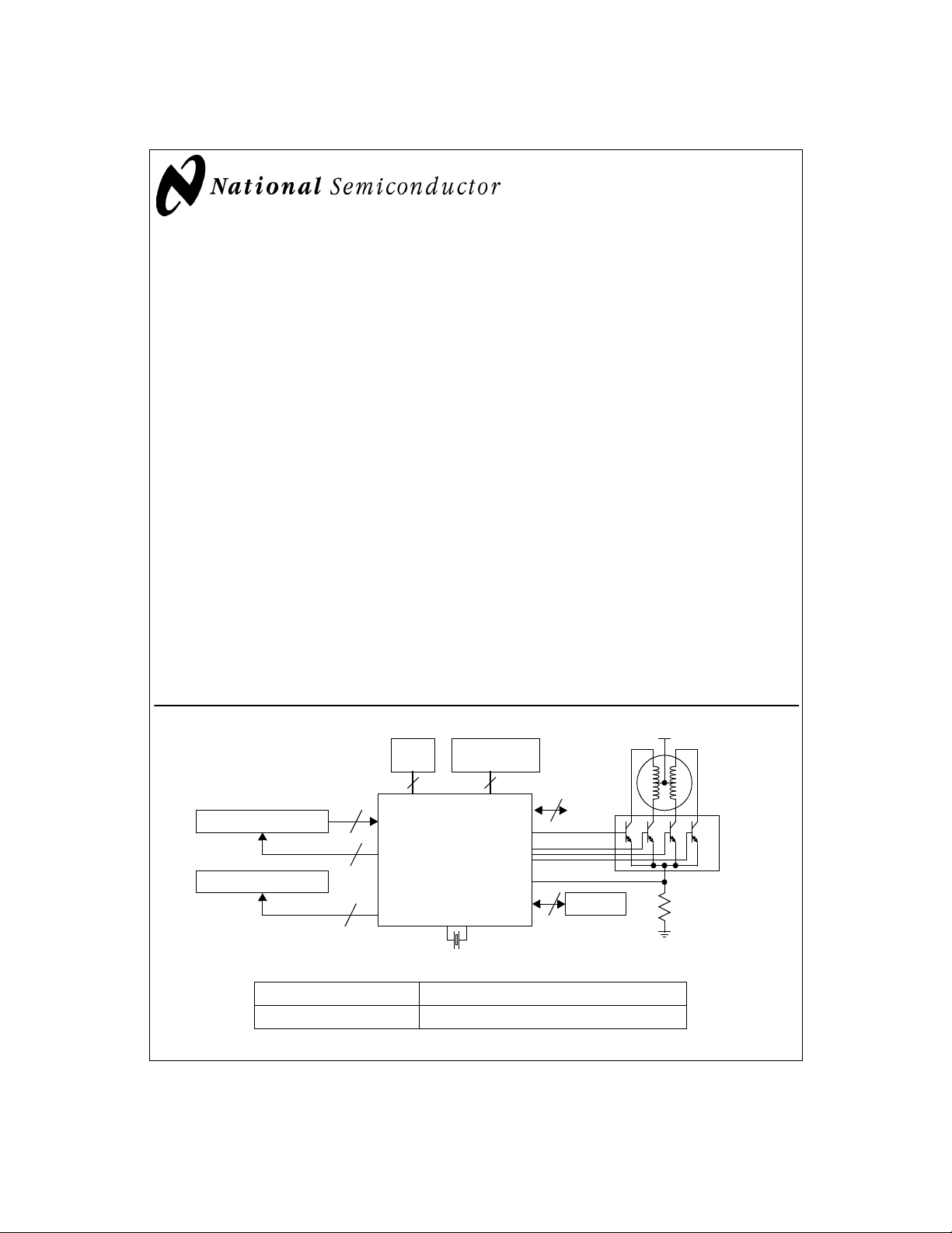
LM9833 Scanner System Block Diagram
USB
Port
2
2-6
1-3
1-3
LM9833CCVJD
CCD/CIS
Illumination
Ordering Information
Commercial (0°C ≤ TA ≤ +70°C) Package
LM9833CCVJ D VJD100A 100 Pin Thin Quad Flatpac
©2000 National Semiconductor Corporation
Serial
EEPROM
2
8MISC
I/O
30
DRAM
48MHz Crystal
1 www.national.com
+12V
Stepper
Motor
Power
Transistors
Page 2
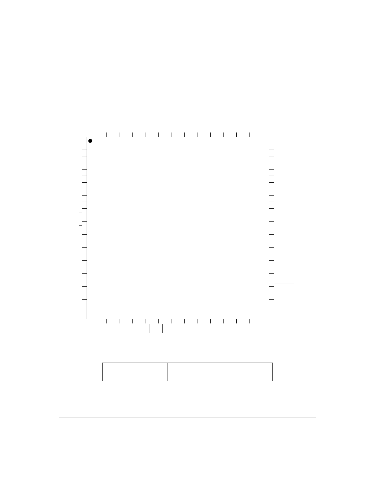
Connection Diagram
LM9833
V
BANDGAP
V
REF LO
V
REF MID
V
REF HI
AGND
V
DGND
OS
OS
OS
D0
D15
DRAM
D1
D14
D2
D13
D3
D12
D4
D11
AGND VADGND VDTEST SENSEGND SENSEA SENSEB NC CMODE RESET NC NC DGND VDBUS POWR D+ D- V
REGULATOR
DGND ACTIVE/SUSPENDED CP2 CP1 RS ø2
100999897969594939291908988878685848382818079787776
1
2
3
R
4
5
G
6
7
B
8
V
9
A
A
10
A
11
B
12
B
13
14
LM9833CCVJD
15
16
17
18
19
20
21
22
23
24
25
75
74
73
72
71
70
69
68
67
66
65
64
63
62
61
60
59
58
57
56
55
54
53
52
51
ø1
TR2
TR1
MISC I/O 6
MISC I/O 5
MISC I/O 4
DGND
V
MISC I/O 3
MISC I/O 2
MISC I/O 1
D
PAPER SENSE 1
PAPER SENSE 2
V
D
DGND
LAMP
B
LAMP
G
LAMP
R
DGND
V
D
24/48
CRYSTAL/EXT CLK
CRYSTAL IN
CRYSTAL OUT
SCL
26 27 28 29 30 31 32 33 34 35 36 37 38 39 40 41 42 43 44 45 46 47 48 49 50
D5
D6
D9
D10
Ordering Information
Commercial (0°C ≤ TA ≤ +70°C) Package
LM9833CCVJD VJD100A 100 Pin Thin Quad Flatpac
DRAM
V
D7
DGND
D8
A9A8A0A7A1
RD
WR
RAS
CAS
A6A2A5A3A4
DRAM
DGND
V
SDA
2 www.national.com
Page 3
Pin Descriptions
USB Interface
D+, D- Digital I/O. USB Interface signals
BUS POWER
ACTIVE/
SUSPENDED
SDA Digital I/O. Serial Data to/from external
SCL Digital Output. Serial Clock Output to externa l
Digital Input. Tie low for bus powered systems, tie high for external power.
Digital Output. Low in Suspend mode. High in
operational mode. Used to control external
regulators, other components.
EEPROM.
EEPROM.
Analog
OSR,
OS
,
G
OS
B
V
REF LO
V
REF MID
V
REF HI
V
BANDGAP
Analog Inputs. The se inpu ts (for Re d, Green ,
and Blue) should be tied to the sensor ’s output signal through DC bloc king capacitors. If
unused, tie to ground through DC blocking
capacitors.
Analog Output/Input . Bypass to AGND with a
0.047µF monolithic capacitor. Do not put a
DC load on this pin.
Analog Output/Input . Bypass to AGND with a
0.047µF monolithic capacitor. Do not put a
DC load on this pin.
Analog Output/Input . Bypass to AGND with a
0.047µF monolithic capacitor. Do not put a
DC load on this pin.
Analog Output. Bypass to AGND with a
0.047µF monolithic capacitor. Do not put a
DC load on this pin.
DRAM
D0 (LSB) -D15
(MSB)
RD
WR
A0-A9 Digital Outputs. Addre ss pins for up to 1M x
RAS
CAS
Digital Inputs/Outp uts. This is the 16 bit data
path between the external DRAM and the
LM9833.
Digital Output. Read signal to external DRAM.
Digital Output. Write signal to external DRAM.
16 external DRAM.
Digital Output. Row Address Strobe signal.
Digital Output. Column Address Strobe sig-
nal.
Scanner Support I/O
PAPER
SENSE 1-2
MISC I/O 1-6 Digital Inputs/Outputs. Programmable, used
Digital Inputs. P rogrammable, u sed for sensing home position, paper, front panel
switches, etc.
for front panel switches, status LEDs, etc. A t
power-on and in Susp end Mode, MISC I/Os
1-3 are inputs and MISC I/Os 4-6 are outputs.
Stepper Motor
A, B, A, B Digital Outputs. Pulses to stepper motor drive
SENSE
A
SENSE
B
SENSE
GND
circuitry.
,
Analog Inputs. Current sensing for stepper
motor’s PWM current control.
Analog Input. Ground sen se input for stepper
motor’s PWM current control.
Sensor Control
ø1 Digital Output. CCD/CIS clock signal phase 1.
ø2 Digital Output. CCD/CIS clock signal phase 2.
RS Digital Output. Reset pulse for the CCD/CIS.
CP1 Digital Output. Clamp pulse for the CCD/CIS.
CP2 Digital Output. Clamp pulse for the CCD/CIS.
TR1, TR2 Digital Outputs. Transfer pulses for the
,
LAMP
R
LAMP
,
G
LAMP
B
CCD/CIS.
Digital Outputs. Us ed to control R, G, and B
LEDs of single output CIS, as well as brightness of CCFL. The CDS signal can be se en
on LAMP
7).
in a test mode (see registe r 5E, bi t
B
Master Clock Generation
CRYSTAL IN Digital Input. Used with CRYSTAL OUT and
CRYSTAL
OUT
CRYSTAL
EXT CLOCK
24/48
an external 48MHz crystal to form a crystal
oscillator.
Digital Output. Used with CRYST AL IN and an
external 48MHz crystal to form a crystal oscillator.
/
Digital Input. Tie to DGND for operati on with
an external crystal. Pull up to V
CRYSTAL OUT with an external TTL or
CMOS clock source.
Digital Input. Tie to DGND for operation with a
48MHz crystal or exter nal clo ck. P ull up to V
for operation with a 2 4M H z crystal o r e xter na l
clock. NOTE: Operation at 24MHz is not guaranteed - always use a 48MHz crystal.
to drive
D
Miscellaneous
V
REGULATOR
RESET Digital input. Take high to force device into
TEST Analog Output.
CMODE Digital Input. Test mode, always tie high.
Digital Output. This is the regu late d 3.3 V supply (generated from V
transceiver. It should be us ed as th e termina l
voltage for the 1.5k D+ pullup resistor, and
bypassed to DGND with a 0.047µF monolithic
capacitor.
Power On Reset state, low to exit reset state.
) that powers the USB
D
LM9833
D
3 www.national.com
Page 4

Pin Descriptions
Analog Power Supplies (4 pins)
LM9833
VA (2) This is the positive supply pin for the analog
AGND (2) This is the ground retu rn for the analog sup-
supply. It should be connected to a voltage
source of +5V and bypassed to AGND with a
0.1µF monolithic capacitor in parallel with a
10µF tantalum capacitor.
ply.
(Continued)
Digital Power Supplies (17 pins)
VD (5) This is the positive su pply pin for the digital
V
(3) This is the positiv e supply pin for the digital
DRAM
DGND (9) This is the ground return for V
supply. It should be connected to a voltage
source of +5V and bypassed to DGND with a
0.1µF monolithic capacitor.
supply for the LM9833’s external DRAM I/O. It
also powers th e A, B , A
outputs. It should be conne cted to a 3 or 5V
supply and bypassed to the closest DGND pin
with a 0.1µF monolithic capacitor.
, and B stepper motor
and V
D
DRAM
.
4 www.national.com
Page 5

LM9833
DRAM
(Notes 1 & 2)
)
+
+0.3V
Operating Ratings
Operating Temperature Range T
LM9833CCVJD 0°C≤T
V
Supply Voltage +4.75V to +5.25V
A
V
Supply Voltage +4.75V to +5.25V
D
V
Supply Voltage +2.85V ≤ V
DRAM
|V
| ≤ 100mV
A-VD
Input Voltage Range -0.05V to V
Absolute Maximum Ratings
Positive Supply Voltage (V+=VA=VD=V
With Respect to GND=AGND=DGND 6.5V
Voltage On Any Input or Output Pin -0.3V to V
Input Current at any pin (Note 3) ±25mA
Package Input Current (Note 3) ±50mA
Package Dissipation at T
ESD Susceptibility (Note 5)
Human Body Model 2000 V
= 25°C (Note 4)
A
Machine Model 250 V
Soldering Information
Infrared, 10 seconds (Note 6) 235°C
Storage Temperature -65°C to +150°
Electrical Characteristics
The following specifications apply for AGND=DGND=0V, VA=VD=V
100%, unless otherwise noted. Boldface limits apply for T
A=TJ=TMIN
Symbol Parameter Conditions
Full Channel Characteristics (in units of 12 bit LSBs unless otherwise noted)
Resolution with No Missing Codes 16 12 bits (min)
DNL
INL
V
OS1
V
OS2
V
OS3
Differential Non-Linear ity
(Note 14)
Integral Non-Lineari ty Error
(Notes 11 & 14)
Analog Channel Gain Constant
C
(ADC Codes/V), referred to 16 bi ts.
Pre-Boost Analog Channel Offset Error 26
Pre-PGA Analog Channel Offset Error -30
Post-PGA Analog Channel Offset Error -26
Bias Current = 80%,
V
DRAM
Bias Current = 80%,
V
DRAM
Includes voltage reference
variation, gain setting = 1
Coarse Color Balance PGA Characteristics (Configuration Registers 3B, 3C, and 3D)
Monotonicity 5 bits (min)
(Minimum PGA Gain) PGA Setting = 0 0.93
G
0
(Maximum PGA Gain) PGA Setting = 31 3.00
G
31
x3 Boost Gain
x3 Boost Setting On
(bit B5 of Gain Register is set)
Gain Error at any gain (Note 13) 0.3
Static Offset DAC Characteristics (Configuration Registers 38, 39, and 3A)
Monotonicity 6 bits (min)
Offset DAC LSB size PGA gain = 1 9
Offset DAC Adjustment Range PGA gain = 1 ±278 ±256 mV (min)
DRAM
=3.3V
=3.3V
=+5.0VDC, f
to T
CRYSTAL IN
; all other limits TA=TJ=25°C. (Notes 8, 9, & 10)
MAX
(Notes 1 & 2)
MIN≤TA≤TMAX
≤+70°C
A
≤ V
DRAM
+100mV
D
+
+ 0.05V
= 48MHz, Analog Bias Current =
Typical
(Note 9)
-0.45
+0.75
-2.3
+1.7
32768
2.94
Limits
(Note 10)
-0.9
+2.4
-8.5
+7.5
29648
37200
-34
+76
-80
+31
-75
+26
0.90
0.96
2.95
3.10
2.85
3.04
-0.6
+0.9
6
12
Units
(Limits)
LSB (min)
LSB (max)
LSB (min)
LSB (max)
LSB (min)
LSB (max)
mV (min)
mV (max)
mV (min)
mV (max)
mV (min)
mV (max)
V/V (min)
V/V (max)
V/V (min)
V/V (max)
V/V (min)
V/V (max)
% (min)
% (max)
mV (min)
mV (max)
5 www.national.com
Page 6

Electrical Characteristics
The following specifications apply for AGND=DGND=0V, V
100%, unless otherwise noted. Boldface limits apply for T
LM9833
(Continued)
A=VD=VDRAM
A=TJ=TMIN
=+5.0VDC, f
to T
CRYSTAL IN
; all other limits TA=TJ=25°C. (Notes 8, 9, & 10)
MAX
Symbol Parameter Conditions
CCD/CIS Source Requiremen ts for Full Spec ified Accura cy and Dynamic Range (Note 12)
V
CCDPEAK
Sensor’s Maximum Outp ut Sig nal
Amplitude before LM9833 Analog Front
End Saturation
Gain = 0.933
Gain = 3.0
Gain = 9.0
Analog Input Characteristics
Average OS
OS
R
, OSG, OSB Input Current CDS Enabled, OS = 3.5V
R
, OSG, OSB Input Current CDS Disabled, OS = 3.5V
DC
DC
Internal Voltage Reference Characteristics
V
BANDGAP
V
REF LO
V
REF MID
V
REF HI
V
REGULA-
TOR
Voltage Reference Output Voltage 1.23 V
Negative Reference Output Voltage V
Midpoint Reference Output Voltage VA/2.0 V
Positive Reference Output Voltage
USB I/O Voltage Regulator 3.3 V
DC and Logic Electrical Characteristics
The following specifications apply for AGND=DGND=0V, VA=VD=V
f
CRYSTAL IN
= 48MHz. Boldface limits apply for TA=TJ=T
MIN
to T
Symbol Parameter Conditions
Digital Input Characteristics for D0-D15 (DRAM Interface)
V
V
V
C
Logical “1” Input Voltage
IN(1)
Logical “0” Input Voltage
IN(0)
Input Leakage Current ±0.1 µA
I
IN
Input Capacitance 5 pF
IN
V
V
V
DRAM
DRAM
DRAM
DRAM
Digital Input Characteristics for PAPER SENSE 1-2, MISC I/O 1-6, SDA, BUS POWER
CMODE
V
V
C
Logical “1” Input Voltage VD=5.25V 2.0 V (min)
IN(1)
Logical “0” Input Voltage VD=4.75V 0.8 V (ma x)
IN(0)
Input Leakage Current ±0.1 µA
I
IN
Input Capacitance 5 pF
IN
Digital Input Characteristics for D+, D-
V
V
C
Logical “1” Input Voltage VD=5.25V 2.0 V (min)
IN(1)
Logical “0” Input Voltage VD=4.75V 0.8 V (ma x)
IN(0)
Input Leakage Current ±0.1 µA
I
IN
Input Capacitance 5 pF
IN
=+5.0VDC unless otherwise noted,
DRAM
; all other limits TA=TJ=25°C. (Notes 8, 9, & 10)
MAX
=5.25V
=3.6V
=4.75V
=2.85V
= 48MHz, Analog Bias Current =
Typical
(Note 9)
1.9
0.6
0.19
Limits
(Note 10)
Units
(Limits)
V
V
V
±3 nA
±26 ±30 µA (max)
-1.0 V
REF MID
V
+1.0 V
REF MID
Typical
(Note 9)
Limits
(Note 10)
2.0
2.0
0.8
0.8
Units
(Limits)
V (min)
V (min)
V (max)
V (max)
, CRYSTAL/EXT CLOCK, 24/48, RESET,
6 www.national.com
Page 7

A=VD=VDRAM
to T
MIN
MAX
(Continued)
=+5.0VDC unless otherwise noted,
; all other limits TA=TJ=25°C. (Notes 8, 9, & 10)
DC and Logic Electrical Characteristics
The following specifications apply for AGND=DGND=0V, V
f
CRYSTAL IN
= 48MHz. Boldface limits apply for TA=TJ=T
Symbol Parameter Conditions
Digital Output Characteristics for D0-D15, A0-A9, RD
V
OUT(1)
V
OUT(0)
Digital Output Characteristics for A, B, A
V
OUT(1)
V
OUT(0)
Logical “1” Output Voltage
Logical “0” Output Voltage
, B
Logical “1” Output Voltage
Logical “0” Output Voltage
, WR, RAS, CAS (DRAM Interface)
V
V
V
V
V
V
V
V
DRAM
DRAM
DRAM
DRAM
DRAM
DRAM
DRAM
DRAM
=4.75V, I
=2.85V, I
=4.75V, I
=2.85V, I
=4.75V, I
=2.85V, I
=4.75V, I
=2.85V, I
OUT
OUT
OUT
OUT
OUT
OUT
OUT
OUT
=-4mA
=-4mA
=4mA
=4mA
=-10mA
=-10mA
=4mA
=4mA
Digital Output Characteristics for MISC I/O 1-6, TR1, TR2, ø1, ø2, RS, CP1, CP2, LAMP
V
V
OUT(1)
OUT(0)
Logical “1” Output Voltage VD=4.75V, I
Logical “0” Output Voltage VD=4.75V, I
=-4mA 2.4 V (min)
OUT
=4mA 0.4 V (ma x)
OUT
Digital Output Characteristics for D+, D-
V
V
OUT(1)
OUT(0)
Logical “1” Output Voltage VD=4.75V, I
Logical “0” Output Voltage VD=4.75V, I
=-1mA 2.4 V (min)
OUT
=3mA 0.4 V (ma x)
OUT
CRYSTAL IN, CRYSTAL OUT Characteristics
XTAL
XTAL
CRYSTAL OUT Bias Level (Offset) 0.8 V
OUT DC
CRYSTAL OUT Amplitude f
OUT AC
= 48MHz 0.8 V
CRYSTAL
Power Supply Characteristics (Note 14)
I
A
I
D
I
DRAM
I
SUSPEND
Analog Supply Current
(V
pins)
A
Digital Supply Current
(V
pins)
D
DRAM Supply Current
(V
pins)
DRAM
Total Suspend Current (IA+ID+I
DRAM
Operating (Bias Current = 80%) 65 91 mA (max)
Operating (Bias Current = 80%) 35 41 mA (max)
Operating, V
Operating, V
DRAM
DRAM
= 5V
= 3V
)19175 µA (max)
Typical
(Note 9)
, LAMPG, LAMP
R
2
1
Limits
(Note 10)
2.4
2.4
0.4
0.4
2.4
2.4
0.4
0.4
B
8
5
LM9833
Units
(Limits)
V (min)
V (min)
V (max)
V (max)
V (min)
V (min)
V (max)
V (max)
P-P
mA (max)
mA (max)
7 www.national.com
Page 8
AC Electrical Characteristics
The following specifications apply for AGND=DGND=0V, VA=VD=V
LM9833
f
CRYSTAL IN
C
= 48MHz, MCLK DIVIDER = 1.0 (unless otherwise noted), f
(databus loading) = 20pF/pin. Boldface limits apply for TA=TJ=T
L
Symbol Parameter Conditions
DRAM Timing (Figure 1)
=5.0V
V
t
RD SETUP
t
RD HOLD
t
WR SETUP
t
WR HOLD
Note 1: Absolute Maximum Ratings indicate limits beyond which damage to the device may occur. Operating Ratings indicate conditions for which the device is functional ,
but do not guara nt ee specific perform ance limits. For g uaranteed specifications and test conditions, see the Electrical Chara cteristics. The gua ranteed specificat ions apply
only for the test conditions listed. Some performance characteristics may degrade when the device is not operated under the listed test conditions.
Note 2: All voltages are measured with respect to GND =AGND=DGND = 0V, unless otherw is e specified.
Note 3: When the input voltage (V
maximum package input current rating limits the number of pins that can simultaneously safely exceed the power supplies with an input current of 25mA to two.
Note 4: The maximum power dissipation must be derated at elevated temperatures and is dictated by T
able power dissipation at any temperature is P
.
is 53°C/W
Note 5: Human body model, 100pF capacitor disch arged through a 1.5 k Ω resistor. Machine model, 200pF capacitor discharged through a 0Ω resistor.
Note 6: See AN-450 “Surface Mounting Methods and Their Effect on Product Reliability” or the section titled “Surface Mount” found in any National Semiconductor Linear
Data Book for other m et hods of soldering su rf ac e mount devices.
Note 7: Two diodes clamp the OS analog inputs to
impedance of the sensor, prevents damage to th e LM9833 from tra ns ients during power-up.
Data valid to RD rising edge
Data valid after RD rising edge 0 ns (min)
Data valid before WR falling edge 5 ns (min)
Data valid after WR rising edge 10 ns (min)
) at any pin exceeds the power supplies (VIN<GND or VIN>VA or VD), the current at that pin should be limited to 25mA. The 50mA
IN
= (TJmax - TA) / ΘJA. TJmax = 150°C for this device. The typical thermal resistance (ΘJA) of this part when board mounted
D
AGND
and VA as shown below. This input protection, in combination with the external clamp capacitor and the output
V
DRAM
DRAM
=3.3V
VA
=+5.0VDC unless otherwise noted,
DRAM
MIN
MCLK
to T
= f
CRYSTAL IN
MAX
/MCLK DIVIDER, f
; all other limits TA=TJ=25°C. (Notes 8, 9, & 10)
Typical
(Note 9)
max, ΘJA and the ambient temperature, TA. The maximum allow-
J
Limits
(Note 10)
26
35
ADC CLK
= f
MCLK
Units
(Limits)
ns (min)
ns (min)
/8,
OS Input
To Internal
Circuitry
AGND
Note 8: For best performance, it is required that all supply pins be powered from the same power supply with separate bypass capacitors at each supply pin.
Note 9: Typicals are at T
Note 10: Tested limits are guaranteed to National's AOQL (Average Outgoing Quality Level).
Note 11: Integral linearity error is defined as the deviation of the analog value, expressed in LSBs, from the straight line that best fits the actual transfer function o f the ADC.
Note 12: V
a white (full scale) image wi th r es pect to the reference level, V
correctable range of pixel-to-pixel V
LM9833 can correct for using its internal PGA.
Note 13: PGA Gain Error is the maximum difference between the measured gain for any PGA code and the ideal gain calculated by using the formula
Gain
Note 14: DNL, INL, and Pow er Supply Current are s pecified at the 80% Bi as Current Setting (R egister 9). This is the ma ximum recomme nded Bias Curren t setting , and
gives the best analog performance as we ll as lower power consu m pt ion for USB-bus powered applications.
is defined as the CCD OS voltage for the reference pe ri od foll o wing the r eset feedthrough pulse. V
REF
V
G0X
--- -
PGA
V
=25°C, f
J=TA
WHITE
PGA code
-------------- ------------ -+=XG
where .
32
= 48MHz, and repre s ent most likely parametric norm.
CRYSTAL IN
is defined as the peak positive deviation above V
. V
REF
variation is defined as the maximum variation in V
–()
31G0
RFT
CCD Output Signal
V
RFT
V
REF
32
------=
31
V
is defined as the peak CCD pixel output voltage for
WHITE
of the reset feedthrough pulse. The maximum
(due to PRNU, light source intensity variation, optics, etc.) that the
WHITE
WHITE
REF
8 www.national.com
Page 9
Timi ng Diagra ms
LM9833
48MHz Internal Clock
(t
= 20.83ns)
PERIOD
A0-A9 Row Address
RAS
CAS
RD
Read Operation
WR
Write Operation
01234560
n
Column Address
t
RD SETUP
n
Row Address
t
RD HOLD
n+1
DataD0-D15
t
t
WR SETUP
WR HOLD
DataD0-D15
Figure 1: DRAM Read and Write
48MHz Internal Clock
(t
= 20.83ns)
PERIOD
RAS
CAS
01234560
Figure 2: DRAM Refresh (CAS
before RAS)
9 www.national.com
Page 10
Register Listing
Registers in bold boxes are reset to that value on power-up. All register addresses are in hexadecimal. All other numbers are
LM9833
decimal unless otherwise noted.
Address Function
IMAGE BUFFER (READ ONLY)
00 Pixel (Image) Data nnnnnnnnOne byte of image data.
STATUS REGISTERS (READ ONLY)
01 Image Data Available In Buffer nnnnnnnn
PAPER SENSE 1 State
read clears bit if edge sensitive input.
PAPER SENSE 2 State
read clears bit if edge sensitive input.
MISC I/O 1 State
read clears bit if edge sensitive input.
MISC I/O 2 State
read clears bit if edge sensitive input.
02
MISC I/O 3 State
read clears bit if edge sensitive input.
MISC I/O 4 State
read clears bit if edge sensitive input.
MISC I/O 5 State
read clears bit if edge sensitive input.
MISC I/O 6 State
read clears bit if edge sensitive input.
DATAPORT REGISTERS
DataPort T arget
DataPort T arget Color
03
Pause (Read Only)
This bit indicates whether or not the scanner
is currently paused due to a buffer full
condition.
DRAM Test
04 DataPort Address - MSB
05 DataPort Address - LSB aaaaaaaa
06 DataPort nnnnnnnn
D7D6D5D4D3D2D1D
0False
1True
0False
1True
0False
1True
0False
1True
0Normal State
1 The scanner is currently in the pause/reverse cycle.
0 Normal Operation
1 DRAM Test mode
R
/Waaaaaa
0
n*2 (256k x 16 DRAM) or n*8 (1M x 16 DRAM)
kilobytes of image data is available
0False
1True
0False
1True
0False
1True
0False
1True
0 0 Offset Coefficient Data
0 1 Gain Coefficient Data
1 0 Gamma Lookup Table
11N/A
00 Red
01 Green
10 Blue
11 N/A
Address of location to be read/written to.
a = 0 to 4095 for gamma tables,
0 to 16383 for Offset and Gain Coefficient Data
Addresses greater than these are illegal.
Bit D6 of register 4 indicates whether next operation
will be a Read (D6=1) or a Write (D6=0).
Data to be read from or written to the address of the
currently selected Dataport Target. The DataPort
Address is automatically incremented whenever one
(gamma data) or two (Gain/Offset Data) bytes are
read from or written to this register.
Value
10 www.national.com
Page 11

MCLK
(Continued)
/8
Register Listing
Address Function
COMMAND REGISTER
Command Register
This register is used to start and end a scan.
It is also used to home the sensor in a
flatbed scanner or eject the image in a
sheetfed scanner. Note: Always make sure
the Command Reg i st er i s in the idle s tat e
(=0) before issuing a new command.
07
Standby
When this bit is set the entire chip enters a
low power state.
Warning: A Standby command will stop
DRAM refresh.
Soft Reset
Write a 1 then a 0 to reset the LM9833’s
state machines.
Warning: A Reset will stop DRAM refresh.
MASTER CLOCK DIVIDER
MCLK Divider
This register sets the master clock frequency
for the entire scanner.
08
f
= 48MHz/MCLK_Divider
MCLK
f
= f
ADC
D7D6D5D4D3D2D1D
0 Normal Operation.
1 Low Power Standby Mode.
0 Normal Operation.
1
000000÷1.0
000001÷1.5
000110÷4
aaaaaa÷ ((aaaaaa/2)+1)
111110÷32.0
111111÷32.5
0
Idle - Stops motor (A, B, A
000
completes current line of data (if scanning).
Note: CCD/CIS clocks continue clocking.
High Speed Forward - Moves motor forward at a
001
speed determined by the Fast Feed Step Size
(registers 48 and 49).
High Speed Reverse - Moves motor backward at a
010
speed determined by the Fast Feed Step Size
(registers 48 and 49).
Start Scan - Resets the LM9833’s data pointers and
011
starts an image scan.
Programmed High Speed Forward - Moves motor
forward at a speed determined by the Fast Feed Step
101
Size (registers 48 and 49) for the number of lines
programmed in registers 4A and 4B.
Programmed High Speed Reverse - Moves motor
backward at a speed determined by the Fast Feed
110
Step Size (registers 48 and 49) for the number of lines
programmed in registers 4A and 4B.
Resets the LM9833. See section 10.2 Soft Reset for
instructions on using this bit.
LM9833
Value
, B = 0),
11 www.national.com
Page 12
Register Listing
Address Function
LM9833
HORIZONTAL RESOLUTION AND DATAMODE SETTINGS
Horizontal DPI Divider
This register determines the horizontal
resolution of the scan.
Scan resolution = Optical resolution divided
by the Horizontal_DPI_Divider.
Pixel Packing
This register determines how many bits in
each byte of data are transmitted to the host
when DataMode = 0
DataMode
09
When DataMode = 0, the pixel data is fully
processed, going through the Offset,
Shading, Horizontal DPI Adjust, Gamma,
and Pixel Packing blocks.
When DataMode = 1, 16 bit da ta is ext racte d
following the Shading Multiplier stage.
Gamma and any other post processing must
be done by th e host.
Analog Bias Current (Percent of Nominal)
The recommended setting is 80% for best
performance. Lower settings will reduce
power consumption further but may degrade
ADC INL and DNL performance.
TURBO AND PREVIEW MODE SETTINGS
Turbo/Preview Mode Select
0A
Turbo/Preview Mode Speed
SENSOR CONFIGURATION
Input Signal Polarity
CDS On/Off
Standard/Even-Odd Sensor
0B
CIS TR1 Timing Mode
Fake Optical Black Pixels
(for Dyna-type CIS sensors)
(Continued)
D7D6D5D4D3D2D1D
0 0 1 bit/pixel (1 bit grayscale/3 bit color)
0 1 2 bits/pixel (2 bit grayscale/6 bit color)
1 0 4 bits/pixel (4 bit grayscale/12 bit color)
1 1 8 bits/pixel (8 bit grayscale/24 bit color)
0
1
0 0 100% (analog supply current = ~81mA)
0 1 80% (analog supply current = ~65mA)
1 0 70% (analog supply current = ~57mA)
1 1 50% (analog supply current = ~41mA)
0 0 Off - use standard CCD Timing
01
10
11 N/A
0 Off: Normal operation
1 On: RS pulse held high for entire Optical Black period
0
000÷1
001÷1.5
010÷2
011÷3
100÷4
101÷6
110÷8
111÷12
1, 2, 4, or 8 bit image data,
as determined by the Pixel Size setting.
16 bit image data - sent in 2 bytes, MSB first:
15 14 13 12 11 10 09 08 - 07 06 05 04 03 02 01 00
0 0 Normal Operation
0 1 Preview Mode (for CCD Sensors)
1 0 Turbo Mode (for CIS Sensors)
11 N/A
00 x2
0 1 x3 (3 Channel Pixel Rate Mode Only)
1 0 x4 (3 Channel Pixel Rate Mode Only)
1 1 x6 (3 Channel Pixel Rate Mode Only)
0 Negative (Most CCD Sensors and Toshiba CIS)
1 Positive (Most CIS Sensors)
0 CDS Off
1 CDS On
0 Standard (1 pixels per Ø period)
1 Even/Odd (2 pixels per Ø period)
CIS TR1 Timing Mode 1:
TR1 pulse = exactly one Ø clock,
starting at rising edge of Ø1
CIS TR1 Timing Mode 2:
TR1 pulse = exactly one Ø clock,
TR1 centered around Ø1 high.
Value
12 www.national.com
Page 13
Register Listing
Address Function
SENSOR CONTROL SETTINGS
Ø1 Polarity
Ø2 Polarity
RS Polarity
0C
CP1 Polarity
CP2 Polarity
TR1 Polarity
TR2 Polarity
Ø1 Active/Off
Ø2 Active/Off
RS Active/Off
CP1 Active/Off
0D
CP2 Active/Off
TR1 Active/Off
TR2 Active/Off
Number of TR Pulses
TR Pulse Duration nnnnn+1 pixel periods (1-16)
0E
TR-Ø1 Guardband Duration n n n n n pixel periods (0-15)
0F Optical Black Clamp Start nnnnn
10 Optical Black Clamp End nnnnn
11 Reset Pulse Start nnnnn
12 Reset Pulse Stop nnnnn
13 CP1 Pulse Start nnnnn
14 CP1 Pulse Stop nnnnn
15 CP2 Pulse Start nnnnn
16 CP2 Pulse Stop nnnnn
17 Reference Sample Position nnnnn
18 Signal Sample Position nnnnn
INTEGRATION TIME ADJUST
19 Integration Time Adjustment Function nnnnnnn
STEPPER PHASE CORRECTION
1A TR to Stepper Phase Correction - MSB nnnnnn
1B TR to Stepper Phase Correction - LSB nnnnnnnn
(Continued)
D7D6D5D4D3D2D1D
0 Positive
1 Negative
0 Positive
1 Negative
0 Positive
1 Negative
0 Positive
1 Negative
0Off
1Active
0Off
1Active
0Off
1Active
0Off
1Active
01 TR Pulse
12 TR Pulses
0
0 Positive
1 Negative
0 Positive
1 Negative
0 Positive
1 Negative
0Off
1Active
0Off
1Active
0Off
1Active
pixel rate: n=0-23, line rate: n=0-7 MCLKs from Ø1 edge
pixel rate: n=0-23, line rate: n=0-7 MCLKs from Ø1 edge
pixel rate: n=0-23, line rate: n=0-7 MCLKs from Ø1 edge
pixel rate: n=0-23, line rate: n=0-7 MCLKs from Ø1 edge
pixel rate: n=0-23, line rate: n=0-7 MCLKs from Ø1 edge
pixel rate: n=0-23, line rate: n=0-7 MCLKs from Ø1 edge
pixel rate: n=0-23, line rate: n=0-7 MCLKs from Ø1 edge
pixel rate: n=0-23, line rate: n=0-7 MCLKs from Ø1 edge
pixel rate: n=0-23, line rate: n=0-7 MCLKs from Ø1 edge
pixel rate: n=0-23, line rate: n=0-7 MCLKs from Ø1 edge
t
= n*t
READOUT
First step of scan occurs n pixels (1 - 16383) after first
TR pulse. This register can be used to set the phase
between the TR pulses and the stepper motor pulses.
NOTE: a setting of n = 0 creates the maximum delay
(16384) pixels, which will increase scan time. If this
function is not used, this register should be set to 1.
Value
, n = 1 to 127. n=0 turns off function.
INT
LM9833
13 www.national.com
Page 14

Register Listing
Address Function
LM9833
(Continued)
D7D6D5D4D3D2D1D
0
Value
SENSOR PIXEL CONFIGURATION
1C Optical Black Pixels Start nnnnnnnnn pixels (0 - 255)
1D Optical Black Pixels End nnnnnnnnn pixels (0 - 255)
1E Active Pixels Start - MSB nnnnnnn pixels (0 - 16383)
1F Active Pixels Start - LSB nnnnnnnn
20 Line End - MSB nnnnnn
21 Line End - LSB nnnnnnnn
Set to the same value as register Data Pixels Sta rt.
n pixels (0 - 16383)
This selects the pixel count at which the current line is
ended and the next line begins. This determines the
integration time of one line.
PIXEL DATA RANGE TO PROCESS
22 Data Pixels Start - MSB nnnnnn
n pixels (Active Pixel s Sta rt - 16383)
This selects the start of the range of pixels transmitted
to the PC and determines the pixel location where
23 Data Pixels Start - LSB nnnnnnnn
offset and shading correction begins (pixel 0 in the
DataPort). This value must be >= Active Pixels Start
24 Data Pixels End - MSB nnnnnnn pixels (Data Pixels Start - [Line End - 20])
25 Data Pixels End - LSB nnnnnnnn
This selects the end of the range of pixels transmitted
to the PC. This value must be <= [Line End - 20]
COLOR MODE SETTINGS
0003 Channel Pixel Rate Color
AFE Operation
3 Channel or 1 Channel
0013 Channel Line Rate Color
1001 Channel Grayscale
1011 Channel Color
1 Channel Grayscale Input Source
(1 Channel Color always uses the
26
Blue Channel as the input)
TR
(=TR1) position
RED
(3 Channel Line Rate Mode only)
TR
(=TR2) position
GREEN
(3 Channel Line Rate Mode only)
TR
(=CP2) position
BLUE
(3 Channel Line Rate Mode only)
3 Channel Line Rate TR
(3 Channel Line Rate Mode only)
3 Channel Line Rate TR
(3 Channel Line Rate Mode only)
27
3 Channel Line Rate TR
(3 Channel Line Rate Mode only)
Triple TR output
RED
GREEN
BLUE
drop
drop
drop
0 0 Red Channel
0 1 Green Channel
1 0 Blue Channel
11 N/A
0 1st TR pulse position (inside Ø1 high)
1 2nd TR pulse position (inside Ø1 low)
0 1st TR pulse position (inside Ø1 high)
1 2nd TR pulse position (inside Ø1 low)
0 1st TR pulse position (inside Ø1 high)
1 2nd TR pulse position (inside Ø1 low)
0 0 Do not drop any TR
01Drop 1 TR
10Drop 2 TR
11N/A
RED
RED
0 0 Do not drop any TR
0 1 Drop 1 TR
1 0 Drop 2 TR
11 N/A
GREEN
GREEN
0 0 Do not drop any TR
0 1 Drop 1 TR
1 0 Drop 2 TR
11 N/A
BLUE
BLUE
pulses
RED
pulse (double integration time)
pulses (triple integration time)
pulses
GREEN
pulse (double integration time)
pulses (triple integration time)
pulses
BLUE
pulse (double integration time)
pulses (triple integration time)
0 Normal operation
1 Outputs single TR pulse on TR1, TR2, and CP2 pins
RESERVED
28 Reserved 00000000Write 00 to this register
14 www.national.com
Page 15

Register Listing
Address Function
(Continued)
D7D6D5D4D3D2D1D
ILLUMINATION SETTINGS
Illumination Mode
Controls t he f u nc t io n of th e 3 L A MP o utp ut s :
LAMP
, LAMPG, and LAMP
R
B
Mode 0 is the Off/Reset state.
Mode 1 is typically used for CCFL lamps.
29
Mode 2 is for color scanning with tri-color
LEDs.
Mode 3 is for grayscale scanning with tricolor LEDs.
LAMP
for INT IME ADJ
B
2A LAMP
2C LAMP
2D LAMP
2E LAMP
2F LAMP
30 LAMP
31 LAMP
32 LAMP
33 LAMP
34 LAMP
35 LAMP
36 LAMP
37 LAMP
PWM - MSB (Illumination Mode 1) nnnnLAMPG output is a PWM pulse stream. Duty cycle is
G
PWM - LSB (Illumination Mode 1) nnnnnnnn
G
On - MSB nnnnnnn pixels (1 - 16384)
R
On - LSB nnnnnnnn
R
Off - MSB nnnnnnn pixels (1 - 16384)
R
Off - LSB nnnnnnnn
R
On - MSB nnnnnnn pixels (1 - 16384)
G
On - LSB nnnnnnnn
G
Off - MSB nnnnnnn pixels (1 - 16384)
G
Off - LSB nnnnnnnn
G
On - MSB nnnnnnn pixels (1 - 16384)
B
On - LSB nnnnnnnn
B
Off - MSB nnnnnnn pixels (1 - 16384)
B
Off - LSB nnnnnnnn
B
STATIC OFFSET AND GAIN SETTINGS FOR ANALOG FRONT END
38 Static Offset (Red)
39 Static Offset (Green)
3A Static Offset (Blue)
3B Static Gain (Red)
3C Static Gain (Green)
3D Static Gain (Blue)
0nnnnnOffset = +n*9.3mV, n = 0 to 31
1nnnnnOffset = -n*9.3mV, n = 0 to 31
0nnnnnOffset = +n*9.3mV, n = 0 to 31
1nnnnnOffset = -n*9.3mV, n = 0 to 31
0nnnnnOffset = +n*9.3mV, n = 0 to 31
1nnnnnOffset = -n*9.3mV, n = 0 to 31
0nnnnnGain = 0.93 + 0.067*n (V/V), n = 0 to 31
1nnnnnGain = 3(0.93 + 0.067*n) (V/V), n = 0 to 31
0nnnnnGain = 0.93 + 0.067*n (V/V), n = 0 to 31
1nnnnnGain = 3(0.93 + 0.067*n) (V/V), n = 0 to 31
0nnnnnGain = 0.93 + 0.067*n (V/V), n = 0 to 31
1nnnnnGain = 3(0.93 + 0.067*n) (V/V), n = 0 to 31
0
= LAMPG = LAMPB = 0V
LAMP
00
R
(Power-On/Reset Default)
Illumination Mode 1 - LAMP
every line, with their on and off points controlled by
the Pixel Counter settings. LAMP
continuous PWM pulse stream. (Figure 20)
01
LAMP
and/or LAMPB may be set to stay on or off at
R
all times by setting the LAMP Off or LAMP On settings
Value
and LAMPB turn on
R
G
(registers 2C-37) grea ter than the Line End value
(registers 20 and 21).
Illumination Mode 2 - LAMP
sequentially at the line rate, with their on and off
10
points controlled by Pixel Counter settings. (Figure
, LAMPG, LAMPB turn on
R
21)
Illumination Mode 3 - LAMP
11
every line, with their on and off points controlled by
, LAMPG, LAMPB turn on
R
the Pixel Counter settings. (Figures 22 and 23)
0LAMP
1
operates normally
B
LAMP
output is enabled during short integration
B
time, low during long integration time.
n/4095. Frequency = 48Mhz/4096 = 11.7kHz2B LAMP
This selects the pixel count at which the LAMP
output goes high (if programmed)
This selects the pixel count at which the LAMP
output goes low (if programmed)
This selects the pixel count at which the LAMP
output goes high (if programmed)
This selects the pixel count at which the LAMP
output goes low (if programmed)
This selects the pixel count at which the LAMP
output goes high (if programmed)
This selects the pixel count at which the LAMP
output goes low (if programmed)
Output is
LM9833
R
R
G
G
B
B
15 www.national.com
Page 16

Register Listing
Address Function
LM9833
DIGITAL PIXEL RATE OFFSET AND GAIN SETTINGS
3E Fixed Offset Coefficient - MSB nnnnnnnn
3F Fixed Offset Coefficient - LSB nnnnnnnn
40 Fixed Multiplier Coefficient - MSB nnnnnnnn
41 Fixed Multiplier Coefficient - LSB nnnnnnnn
DIGITAL PIXEL RATE OFFSET AND GAIN/DRAM SETTINGS
Shading Multiplier
Multiplier Coefficient Source
42
Offset Coefficient Source
Reserved 1 0 Set to 10
DRAM Size
(Continued)
D7D6D5D4D3D2D1D
0 256k x 16
11M x 16
0
Fixed Offset to use for calibration
Fixed Gain to use for calibration
0 Gain = [Multiplier Coefficent]/16384
1 Bypass Multiplier
0 Configuration Register 40 and 41 (Fixed)
1 External DRAM
0 Configuration Register 3E an d 3F (Fixed)
1 External DRAM
Value
16 www.national.com
Page 17

Register Listing
Address Function
STEPPER MOTOR CONTROL SETTINGS
n (Line Skipping)
43
Part of the “n out of m” function, consisting of
registers 43, 44, and 54 (bits 3-7).
m (Line Skipping)
44
Part of the “n out of m” function, consisting of
registers 43, 44, and 54 (bits 3-7).
Full/Microstepping
Current Sensing Phases
= 0 for fullstepping
= 1 for micros tepping
Stepper Motor Phase A Polarity
45
Stepper Motor Phase B Polarity
A, B, A
Swap A/A
(Reverses m otor directi on)
Fullstep During FastFeed at Start of Scan
46 Scanning Step Size - MSB nnnnnnnnThe step size of one microstep while scanning, in
48 Fast Feed Step Size - MSB nnnnnnThe step size of one microstep while fast feeding, in
4A Fullsteps to Skip at Start of Scan - MSB nnnnnnnWhen scan starts, paper is fed forward n full steps (0 -
4C Step Counter - MSB nnnnnnCounts n (0-16383) full steps. See register 58, bit 5
4E Pause scanning, stop/reverse motor nnnnnnnn
4F Resume scanning, start motor nnnnnnnn
50 Full steps to reverse when buffer is full nnnnnnnnn (0-255) full steps (0 = do not reverse)
Acceleration Profile (stopped) n n n (0,1, 2, or 8) f ull st ep t ime un i ts pa us e whi le s top pe d
Acceleration Profile (25%) n n n (0,1, 2, or 8) full steps at 25% speed
51
Acceleration Profile (50%) n n n (0,1, 2, or 8) full steps at 50% speed
Default Phase Difference - High Byte n n 18 bit word used to calculate when motor resumes
52 Default Phase Differen ce - Mid B yte nnnnnnnn
53 Default Phase Difference - Low Byte nnnnnnnn
Lines to Process After Pa us e/
Lines to Discard after Resum e
Line Skipping Phase
Part of the “n out of m” function, consisting of
54
registers 43, 44, and 54 (bits 3-7).
Line Skipping Color Phase Delay
Part of the “n out of m” function, consisting of
registers 43, 44, and 54 (bits 3-7).
(Continued)
, and B stepper motor status
with B/B
D7D6D5D4D3D2D1D
tttttttt
mmmmmmmm
0 A, B, A
1A, B, A
0 Default polarity
1 Reverse Polarity
0 Traditional Operation
1 Fullstep during fastfeed at start of scan
n n n n n lines, n = 0-15
0
n lines saved in DRAM for every m lines (register 44)
scanned, function bypassed if register value = 0.
n (lines saved per m lines scanned) = 256 - t
t = 256 - n
If t = 0 then function is bypassed.
n lines (register 43) saved in DRAM for every m lines
scanned. m = 1 to 255.
If m = 0 then function is bypassed.
0 Full Step Mode
1 Microstepping Mode
1 Phase - No microstepping, just kickstart/stop
0
functions
1 2 Phases - necessary for microstepping
0
Positive (A/B/A
Negative (A/B/A
WARNING: When idle, this setting leaves the motor
1
energized for unipolar motors, and will destroy bipolar
0
1
0 Red sensor data arrives before Green sensor
1 Blue sensor data arrives before Green sensor
motor drivers. Keep this bit set to a 0.
Positive (A/B/A
Negative (A/B/A
WARNING: When idle, this setting leaves the motor
energized for unipolar motors, and will destroy bipolar
motor drivers. Keep this bit set to a 0.
, and B output pins in Tri-State
, and B output pins active
units of pixel periods (minimum 2)47 Scanning Step Size - LSB nnnnnnnn
units of pixel periods (minimum 2)49 Fast Feed Step Size - LSB nnnnnnnn
32767) at highest speed. For “zooming” in flatbeds4B Fullsteps to Skip at Start of Scan - LSB nnnnnnnn
for more information.4D Step Counter - LSB nnnnnnnn
Pause scan when buffer is n*2 (16 x 256k) or
n*8 (16x1M) kbytes full
Resume scan when buffer is n*2 (16 x 256k) or
n*8 (16x1M) kbytes full
after reversing and stopping. 1 < n < 262143. 2 bits in
register 51 are the most significant bits of 18 bit word.
n (0-7) lines. This only applies if the motor doesn’t
nnn
reverse (reverse steps = 0)
Value
/B Output high = winding energized)
/B output low = winding energized)
/B Output high = winding energized)
/B output low = winding energized)
LM9833
17 www.national.com
Page 18

Register Listing
Address Function
LM9833
Kickstart steps (fullstepping mode) nnnMotor gets maximum current for first n (0-7) full steps
55
Hold Current Timeout nnnnn Full step time units (1-31) (do not set to 0)
56 Stepper Motor PWM Frequency nnnnnnnn
57 Stepper Motor PWM Set Duty Cycle nnnnnn= minimum of n/64 (default = 0)
PAPER SENSE SETTINGS
PAPER SENSE 1: Polarity
PAPER SENSE 1: Level/Edge sensitive
PAPER SENSE 1: Stop Scan, High Speed
Forward, and H igh Speed Reverse
Use this input for the home sensor in flatbed
scanners.
PAPER SENSE 2: Polarity
58
PAPER SENSE 2: Level/Edge sensitive
PAPER SENS E 2: Stop Scan and High
Speed Forward
(Continued)
D7D6D5D4D3D2D1D
0
1
0
1
0 A low input on PAPER SENSE 2 is True
1 A high input on PAPER SENSE 2 is True
0
1
0
1
0
=CRYST AL OUT/(256*n) (0 < n < 256)
=CRYSTAL OUT/(256*256) (n = 0)
0 A low input on PAPER SENSE 1 is True
1 A high input on PAPER SENSE 1 is True
Level sensitive: PAPER SENSE 1 State bit (in Status
Register) is set to a 1 if PAPER SENSE 1 is currently
True.
Edge sensitive: PAPER SENSE 1 State bit (in Status
Register) is set to a 1 if PAPER SENSE 1 has been
True since the last time the Status Register was read.
Transitions on PAPER SENSE 1 will not clear the
command register.
A False-to-True transition on P APER SENSE 1 will
clear the Command Register and stop the scan .
Level sensitive: PAPER SENSE 2 State bit (in Status
Register) is set to a 1 if PAPER SENSE 2 is currently
True.
Edge sensitive: PAPER SENSE 2 State bit (in Status
Register) is set to a 1 if PAPER SENSE 2 has been
True since the last time the Status Register was read.
The scan will automatically stop after scanning for the
number of fullsteps specified in the Step Counter
(registers 4C and 4D). (The fullsteps moved during
the “FastFeed At Start of scan period are not
counted.) If the value in the Step Counter is 0, the
scan can only be stopped by writing a 0 to register 07.
A False-to-True transition on P APER SENSE 2 will
stop a scan or a High Speed Forward command after
the number of fullsteps specified in the Step Counter
(registers 4C and 4D). It will not stop a High Speed
Reverse, and therefore should not be used as a home
position s ensor input.
Value
18 www.national.com
Page 19

Register Listing
Address Function
MISC I/O PIN SETTINGS
MISC I/O 1: Input or Output
MISC I/O 1: Polarity
(if configured as an input)
MISC I/O 1: Level/Edge sensitive
(if configured as an input)
MISC I/O 1: Output State
(if configured as an output)
Power On/USB Suspend Default: Input
59
MISC I/O 2: Input or Output
MISC I/O 2: Polarity
(if configured as an input)
MISC I/O 2: Level/Edge sensitive
(if configured as an input)
MISC I/O 2: Output State
(if configured as an output)
Power On/USB Suspend Default: Input
MISC I/O 3: Input or Output
MISC I/O 3: Polarity
(if configured as an input)
MISC I/O 3: Level/Edge sensitive
(if configured as an input)
MISC I/O 3: Output State
(if configured as an output)
Power On/USB Suspend Default: Input
5A
(NEW)
MISC I/O 4: Input or Output
MISC I/O 4: Polarity
(if configured as an input)
MISC I/O 4: Level/Edge sensitive
(if configured as an input)
MISC I/O 4: Output State
(if configured as an output)
Power On/USB Suspend Default: Output,
Logic High
(Continued)
D7D6D5D4D3D2D1D
0 The MISC I/O 2 pin is configured as an input.
1 The MISC I/O 2 pin is configured as an output.
0 A low input on MISC I/O 2 is True
1 A high input on MISC I/O 2 is True
0
1
0
1
0 The MISC I/O 4 pin is configured as an input.
1 The MISC I/O 4 pin is configured as an output.
0 A low input on MISC I/O 4 is True
1 A high input on MISC I/O 4 is True
0
1
0
1
0
0 The MISC I/O 1 pin is configured as an input.
1 The MISC I/O 1 pin is configured as an output.
0 A low input on MISC I/O 1 is True
1 A high input on MISC I/O 1 is True
Level sensitive: MISC I/O 1 State bit (in Status
0
Register) is set to a 1 if MISC I/O 1 is currently True.
Edge sensitive: MISC I/O 1 State bit (in Status
1
Register) is set to a 1 if MISC I/O 1 has been True
since the last time the Status Register was read.
0
1
0
1
The output of the MISC I/O 1 pin will be a logic low
(0V).
The output of the MISC I/O 1 pin will be a logic high
(5V).
Level sensitive: MISC I/O 2 State bit (in Status
Register) is set to a 1 if MISC I/O 2 is currently True.
Edge sensitive: MISC I/O 2 State bit (in Status
Register) is set to a 1 if MISC I/O 2 has been True
since the last time the Status Register was read.
The output of the MISC I/O 2 pin will be a logic low
(0V).
The output of the MISC I/O 2 pin will be a logic high
(5V).
0 The MISC I/O 3 pin is configured as an input.
1 The MISC I/O 3 pin is configured as an output.
0 A low input on MISC I/O 3 is True
1 A high input on MISC I/O 3 is True
Level sensitive: MISC I/O 3 State bit (in Status
0
Register) is set to a 1 if MISC I/O 3 is currently True.
Edge sensitive: MISC I/O 3 State bit (in Status
1
Register) is set to a 1 if MISC I/O 3 has been True
since the last time the Status Register was read.
The output of the MISC I/O 3 pin will be a logic low
(0V).
The output of the MISC I/O 3 pin will be a logic high
(5V).
Level sensitive: MISC I/O 4 State bit (in Status
Register) is set to a 1 if MISC I/O 4 is currently True.
Edge sensitive: MISC I/O 4 State bit (in Status
Register) is set to a 1 if MISC I/O 4 has been True
since the last time the Status Register was read.
The output of the MISC I/O 4 pin will be a logic low
(0V).
The output of the MISC I/O 4 pin will be a logic high
(5V).
Value
LM9833
19 www.national.com
Page 20

Register Listing
Address Function
LM9833
MISC I/O 5: Input or Output
MISC I/O 5: Polarity
(if configured as an input)
MISC I/O 5: Level/Edge sensitive
(if configured as an input)
MISC I/O 5: Output State
(if configured as an output)
Power On/USB Suspend Default: Output,
5B
Logic High
(NEW)
MISC I/O 6: Input or Output
MISC I/O 6: Polarity
(if configured as an input)
MISC I/O 6: Level/Edge sensitive
(if configured as an input)
MISC I/O 6: Output State
(if configured as an output)
Power On/USB Suspend Default: Output,
Logic Low
TEST MODE SETTINGS
5C ADC Output Code - MSB nnnnnnnnUsed to force the input to the HDPI Divider to a known
ADC Test Mode
Pixel Processing Input Select
5E
16 bit Counter Increment Select
(16 bit counter starts at 0, increments every
datapixel)
MCLK edge for AFE (Set this bit to 0)
CDS Signal
5F-68 Reserved 00000000Write 00 to these registers
69 Version Number 100
6A-7F Reserved 00000000Write 00 to these registers
(Continued)
D7D6D5D4D3D2D1D
0 The MISC I/O 6 pin is configured as an input.
1 The MISC I/O 6 pin is configured as an output.
0 A low input on MISC I/O 6 is True
1 A high input on MISC I/O 6 is True
0
1
0
1
0 0 Increments by 1
0 1 Increments by 4
1 0 Increments by 16
11 N/A
0 Rising
1 Falling
0 Normal Operation
1 CDS signal is output on LAMP
0
0 The MISC I/O 5 pin is configured as an input.
1 The MISC I/O 5 pin is configured as an output.
0 A low input on MISC I/O 5 is True
1 A high input on MISC I/O 5 is True
Level sensitive: MISC I/O 5 State bit (in Status
0
Register) is set to a 1 if MISC I/O 5 is currently True.
Edge sensitive: MISC I/O 5 State bit (in Status
1
Register) is set to a 1 if MISC I/O 5 has been True
since the last time the Status Register was read.
0
1
0 0 Normal Operation - ADC Output
0 1 Registers 5C and 5D
1 0 16 bit counter, reset at the start of every scan
1 1 16 bit counter, reset at the start of every line
The output of the MISC I/O 5 pin will be a logic low
(0V).
The output of the MISC I/O 5 pin will be a logic high
(5V).
Level sensitive: MISC I/O 6 State bit (in Status
Register) is set to a 1 if MISC I/O 6 is currently True.
Edge sensitive: MISC I/O 6 State bit (in Status
Register) is set to a 1 if MISC I/O 6 has been True
since the last time the Status Register was read.
The output of the MISC I/O 6 pin will be a logic low
(0V).
The output of the MISC I/O 6 pin will be a logic high
(5V).
value for digital tests5D ADC Output Code - LSB nnnnnnnn
0 0 Normal Operation
0 1 Bypass AFE, Normal ADC Operation
Bypass AFE, bypass ADC digital corre ction,
10
output uncorrected ADC MSB
Bypass AFE, bypass ADC digital corre ction,
11
output uncorrected ADC LSB
100 = LM9832 or LM9833
(011 = LM9831, 010 = LM9830)
Value
B
pin
20 www.national.com
Page 21

Applications Information
1.0 OVERVIEW
The LM9833 is a USB, 1200d pi, 16 bit (48 bit colo r) scanner- ona-chip. The LM9833 is an improved, 16 bit version of the
LM9831, providing all o f the L M9 831 ’s functionality while impr oving performance and adding several new features. See 12.0
CHANGES FROM THE LM9831 for a complete list of additions
and enhancements.
2.0 ANALOG SIGNAL PROCESSING
One channel of the LM9833’s analog front end is shown in Figure
3. The gain through each cha nnel can be set between 0.93V/V
and 9.0V/V using regi sters 3B, 3C , and 3D. Th e offset DAC p rovides up to ±278mV of offset correction using registers 38, 39,
and 3A. The offset DAC an d ga i n s tage s sh ould be adjusted during coarse calibration so that the input signal is a maximum of
1.9Vp-p at the ADC input.
3.0 DIGITA L SIGNAL PROCESSING
3.1 ADC
The digital pixel data comes from a 6MHz 16 bit pipelined ADC.
3.2 Pixel Processing Block
The Pixel Processing stage is used to digit ally re duce t he optica l
resolution of the sensor. The optical resolution can be reduced by
a factor of 1, 1.5, 2, 3, 4, 6 , 8, o r 1 2. For a 12 00 d pi (o ptica l) system, this would prod uce res olutions o f 1200 , 800, 6 00, 40 0, 300 ,
200, 150, and 100. A 600 dpi (optical) system would be cap able
of 600, 400, 300, 200, 150, 100, 75, and 50 dpi. (Resolution in the
vertical direction is controlled by the stepper motor speed.)
Horizontal resolution reduction is accomplished by averaging
adjacent pixels. Averaging produces better image quality and
reduces aliasing versus the traditional technique of simply discarding pixels to r educe resolutio n. For example , to get 100 dp i
from a 300dpi optical sensor, you would average 3 300dpi pixels:
p
++
pixel
100dpi
n-2pn-1pn
-------------------- ----------------------- -=
3
The number of pi xe ls co ming o ut of the Pixel Processing block is
equal to the integer portion of the number of pixels going in to the
Pixel Processing block divided by the “Divide By” setting, from the
table shown in Figure 4.
Pixels
IN
OUT
=
INT
------------------- ------
Divide By
Pixels
This equation also applies to the divide by 1.5 function.
Divide
By
DPI
(1200
DPI
system)
DPI
(800
DPI
system)
DPI
(600
DPI
system)
DPI
(300
DPI
system)
1 1200 800 600 300
1.5 800 533 400 200
2 600 400 300 150
3 400 267 200 100
4 300 200 150 75
6 200 133 100 50
8 150 100 75 37.5
12 100 67 50 25
Figure 4: Decrea sing Horizo nta l Resolutio n
If there are not enough pixe ls at the end of a line to fo rm a complete pixel, the last pixel will be eliminated . For example, if a line
is 35 pixels wide and the Horizontal DPI setting i s set to divide by
6, then the output of the Pixel Processing block will be 5 pixels
(the integer portion of 35/6). The last 5 pixels will be discarded,
since 6 pixels would be required to form a new pixel in this mode.
The output of this stage is sent to the Pixel Rate Offset Correction
Block.
3.3 Pixel Rate Offset Correction Block
Offset correction words for every pixel of the CCD are stored in
LM9833
Σ
+
V
DAC
OS1)GB
PGA
0.93V/V t o
3V/V
G
PGA
+ V
DAC
+ V
+
+
V
Σ
OS3
OS2)GPGA
+ V
16 Bit
ADC
OS3
D
OUT
)C
Gain Boost
1V/V or
3V/V
+
+
V
IN
G
Σ
+
V
OS1
B
D
OUT
= (((VIN + V
+
Σ
+
V
OS2
Offset
DAC
simplified, with all offsets = 0, this is:
D
= (VINGB + V
OUT
DAC)GPGA
C
C is a constant that combines the gain error thr ough th e AFE, ref erence voltage var ianc e, and ana log voltage
to digital code conversion into one constant. Ideally, C = 32768 codes/V.
Manufacturing tolerances widen the range of C. See Electrical Specifications.
Figure 3: Analog Front End (AFE) Model
21 www.national.com
Page 22

Applications Information
(Continued)
the external DRAM and accessed at the pixel rate . A digital subtractor subtracts the 16 bit offset word (corresponding to that
LM9833
pixel’ s offset error) from each pixel.
The subtractor saturates at 0, i.e. if the coefficient to be sub-
tracted is greater than the ADC output code, the result is an output of 0.
The offset words stored in DRAM are typically calculated by
scanning a black calibration strip at 16 bits, and storing the
results in the DRAM using the DataPort.
The offset correction equation is:
Pixel
PixelINcoefficient
=
OUT
–
3.6 Pixel Packing/Thresholding Block
Some scans require only one bit per pixel (“line art” mode), others
may need only 2 or 4 bits/ pixel. To increase scanning speed for
lower pixel depths, the LM9833 packs the desir ed MSBs of multiple pixels together into 1 16 bit word, increasing the transmission
speed to the host by a factor of 2, 4, 8, or 16. Figure 6 shows how
the pixels are packed together f or 8, 4, 2, an d 1 bit pixel depths.
In Figure 6, “b” indicates the bit position (b7 = the most significant
and b0 = the least significant bit) of the original 8 bit pixel data,
and p
indicates the original pixel sequence, i.e p0, p1, p2, p3...
n
If there are no t enough unpacked pixe ls at the end of a line to
complete the packed wor d for t ransmiss ion, tha t final wor d is not
sent. For exampl e, doing an 8 bit pixel rate scan with a HDPI
divider of 1 and an odd number of pixels will truncate the blue
component of the last pixel.
3.4 Pixel Rate Gain Correction Block
This is a digital multiplier that multiplies the outp ut word from the
subtractor by a 16 bit di gital correcti on coefficient corres ponding
to that pixel’s gain err or. The coefficients are stored in the external RAM and accessed at the pixel rate.
The multiplier saturate s at 65535, i.e. if the result of the m ultiplication is greater than 65535, the multiplier output is 65535.
The gain equation is:
coefficient
----------------- --------- -
Pixel
OUT
=
Pixel
⋅
IN
16384
Note that a c o ef f i ci en t of 0 r ep r es e nt s a g ai n of 0. O n t he LM98 3 0
and previous parts, a coe fficient of 0 re presented a gain o f 1. To
achieve a gain of 1, the coefficient should be set to 16384.
3.5 Gamma Correction Tables
There are 3 gamma loo kup tables for R, G, and B. The inp ut to
the table is the 12 MSBs ( most si gnifican t bit s) of th e 16 b it pixe l
data coming from t he previous st age (3.4 P ixel Rate Gain Cor-
rection Block). The output is the 8 bit gamma corrected pixel
data. The tables consume 12k words (4K bytes x 16 bits, only the
8 LSBs of each word is used) of the external DRAM. Each
gamma table (red, gre en, an d blu e) can b e loa ded with a ny a rbitrary user-defined transfer curve.
255
Pixel
Depth
bit15bit14bit13bit12bit11bit10bit9bit
8b7 p
4b7 p0b6 p0b5 p0b4 p0b7 p1b6 p1b5 p1b4 p
b6 p0b5 p0b4 p0b3 p0b2 p0b1 p0b0 p
0
2b7 p0b6 p0b7 p1b6 p1b7 p2b6 p2b7 p3b6 p
1b7 p0b7 p1b7 p2b7 p3b7 p4b7 p5b7 p6b7 p
bit 7 bit 6 bit 5 b it 4 bit 3 bit 2 bit 1 bit 0
8b7 p
4b7 p2b6 p2b5 p2b4 p2b7 p3b6 p3b5 p3b4 p
b6 p1b5 p1b4 p1b3 p1b2 p1b1 p1b0 p
1
2b7 p4b6 p4b7 p5b6 p5b7 p6b6 p6b7 p7b6 p
1b7 p8b7 p9b7 p10b7 p11b7 p12b7 p13b7 p14b7 p
8
0
1
3
7
1
3
7
15
Figure 6: Packing Multiple Pixels Into One Word
The gamma table in 3.5 Gamma Correct ion Tables allows the
user to set the threshol d of each transi tion for various l ine art or
reduced pixel depth modes.
3.7 16 Bit Output Mode
The LM9833 als o sup p or t s a 16 b i t o ut m o de . Th i s c a n be us ed t o
get very accurate data for calibration o r to scan a 16 gr ay/48 bit
color image. This mode i s set through regist er 9, bit 5. In the 16
bit output mode, the gamma and pixel packing stages are
bypassed, and the 16 bit da ta from the ADC is st ored in DRAM,
formatted as shown in Figure 7.
MSB 151413121110 9 8
b15 b14 b13 b12 b11 b10 b9 b8
LSB76543210
b7 b6 b5 b4 b3 b2 b1 b0
Figure 7: 16 Bit Output Mode Data Format
8 Bit Pixel Out
0
12MSBs of 16 bit Output
0 4095
Figure 5: Gamma Table
The gamma tables are loa ded thr ough th e da taport ( see 6.1 The
DataPort: Reading and Writing to Gamma, O ffset, and Gain
Memory). The DataPort selects which color (Red, Green or Blue)
gamma table will be read from or written to.
The memory reserved for the gamma table is used to store image
data in the 16 bit mode. After scanning in 16 bit mode, the
gamma table mus t be reloaded f or operation in 8, 4, 2, or 1 bi t
mode.
3.8 Line Buffer
The line buffer uses the external DR AM as a FIF O line buffer to
store the pixel data (wh ich is generated at a fi xed rate, synchronous to the CCD clocks) and send it back to the PC at an as ynchronous, unpredictable, and non-constant rate.
The LM9833 supports 2 sizes of DRAM, 2 56k x 16bit and 1M x
16bit. 216kbytes (108kwords) of the capacity of the DRAM is con-
22 www.national.com
Page 23

Applications Information
sumed by the offset and shading coefficients an d the gamma
tables. That leaves 296k bytes of m emory av ailabl e for line bu ffer
when using a 256k x 16 bit DRAM, or 1832kbytes of memor y
when using a 1M x 16 bit DRAM.
The line buffer is tightly co upled to th e stepper mo tor (4.0 Step-
per Motor Control ler ), and is res ponsibl e for stoppi ng the motor
before the buffer overflows and starting the motor again as the
buffer nears empty.
If the scanner is generating pixe l data faster than the PC can
acquire it, the line buffer will start to fill up. As the buffer nears
100% of its capacity, the scan must be paused before it starts
acquiring a line which will overflow the buffer. This Pause Threshold limit (register 4 E) is program mable in 2 kbyte (256k x 16 bi t
DRAM) or 8kbyte (1M x 16 bit DRAM) increme nts be twee n 0 and
255.
To maximize scanner perfo rmance and min imize pausing d ue to
buffer full conditions, the pause threshold should be set using this
formula:
Pause Threshold (kB) = Available_Memory - (Line_Length + 1)
where Available_Memory = 296kbytes (256k x 16b DRAM) or
1832kbytes (1M x 16 bit D RAM),
Line_Length = (Bytes/Line)/1024
INT
Bytes/Line 2 INT
Where C = 1 for “1 Channel Grayscale”, 3 for all other modes,
Data_Pixels = Data Pixels End (regi sters 24, 25) - Data Pixels
Start (registers 22, 23)
HDPI_Divider = Horizontal DPI divider = 1, 1.5, 2, 3, 4, 6, 8, or 12
B = Bits per Pixel = 16 (16 bit mode), 8, 4, 2, or 1
Register 4E value = Pause Thre shold (kB)/2 (256k x 16 DRA M)
or Pause Threshold (kB)/8 (1M x 16 DRAM)
When the Pause Thresho ld is reached the b uffer sends a com-
mand to the stepper motor controller to stop scanning. The
remainder of the line being processed will continue being processed and be sent to the buffer. If the Lines To Process After
Pause Scan Signal register (regis ter 54) is great er than 0, then
room for these additional lines nee ds to be added into the Pause
Threshold value calculation.
Note that the scanner software on th e host PC mu st set a Pause
Threshold value low eno ugh to ensure tha t any data that come s
after a pause request (the rest of the curre nt line and any sub sequent lines if register 54 bits 0-2 are greater than 0) will fit into the
DRAM buffer. If the Pause Threshold is set too high, the Line
Buffer may overflow, creating discontinuities in the scanned
image.
After a pause, the buffer will continue to transmit data to the PC
until it hits the Resume Threshold limit (register 4F), which is also
programmable in 2 kbyt e (256k x 16 bi t DRAM) or 8kb yte (1M x
16 bit DRAM) increments between 0 and 255. When the Resume
Threshold is reached, the Line Buffer sends the motor controller a
command to resume.
4.0 Stepper Motor Controller
The stepper motor controller sends a series of pulses to the step-
=
⋅
------------------- ------------------------------ ---------------------- -
(Continued)
Data Pixels
------------------- ---------------- -
HDPI_Divider
CB⋅⋅
16
per motor to move the pap er past the sensor (sheetfed) or the
sensor past the paper (flat bed). The speed at which the paper
moves relative to the sensor, combined with the i ntegration t ime
of the image sensor, determines the effective vertica l resolution
(Lines Per Inch, or LPI).
The stepper motor i s mo ved for w ard s a nd backwards by two signals, A and B, 90° out of ph ase with each other. The phase for
the forward direction is set in Configuration Register 45.
The A and B signals are e ither square waves (in F ull Step Mo de,
Figure 8), or a staircase approximation of a sine wave (in
Microstep mode, Figures 10 and 11).
A
A
1 full step = 4
microsteps
B
B
Figure 8: Stepper Motor Waveform - Full Stepping
The LM9833 always counts stepper motor steps in units of
microsteps. A full step is equal to four microsteps. Even when the
LM9833 is in Full Step Mode, it is counting in microsteps, and will
increment the stepper motor (generating a full step) every fo ur
microsteps.
The microstep Step Size is defined in units of time. These units of
time are pixel periods , as defined in the hor izontal pixel coun ter.
In the 3 Channel Pixel Rate input mode, the pixel period is the
f
/3 (= f
ADC
modes, the pixel period is eq ual to f
Size is stored in the Scanning S tep Size confi guration register
as a 14 bit value. During normal operation, the stepper motor is
advanced 1 microstep every Step Size pixel periods. The LPI can
be calculated as follows:
Where FSPI = the number of full steps required to move the
image one inch, pixels/l ine is the nu mber of pixel pe riods it takes
to scan one horizo ntal line (e quivalent to the value stor ed in the
Line End registers), StepSize is the number of pixel periods/microstep, and X = 3 for line rate and 1 for pixel rate modes.
Whenever the stepper motor has been moving and then comes to
a stop, the LM9833 waits for the time specified in the Hold Current Timeout register a nd th en de -asserts the A, B, A
puts to cut power t o the motor. When the stepper m otor is not
scanning or fast-feeding (Command = 00), A, B, A
asserted in all stepper modes.
There are two modes of stepper motor operation: fullstepping and
microstepping.
4.1 Full Step Mode
In Full Step Mode the out put is a pulse str eam, as shown i n Figure 8. The amplitude of the pul ses is controlled by the outp ut of
/24). In the 3 Channe l Line Rate and 1 channe l
MCLK
LPI 4FSPI
----------------- ------------------ -=
pixels/line X
ADC
StepSize
(= f
⋅
/8). The Step
MCLK
, and B are de-
, and B out-
LM9833
23 www.national.com
Page 24

Applications Information
the 2 bit DAC, shown in Figure 9.
(Continued)
LM9833
Scan Mode DAC Voltage
Starting from
a dead stop
Scanning 0.347V
Stopped
4.2 Microstep Mode
Microstepping is a techni que of driving the stepper motor with a
staircase approximation of a si ne wave, as shown in Figure 10 .
This technique maximizes the torque of a given motor, resulting in
a higher maximum speed. In additi on, it increases the reso lution
of the stepper motor. If a stepper motor moves 3.6° per full step,
microstepping can crea te positions inside the 3.6°: 1.8°, 0.9° , or
0.45°, for example. Th is increases the maximu m vertical resolution of the scan ner. Microstepping also results in q uieter motor
movement.
A
A
B
0.484V for number of steps specified
in Kickstart Steps register (0-7). If
register is 0 there is no Kickstart
current-movement begins at 0.347V.
0.133V for number of steps specified
in Hold Current Timeout register (1 -
31), 0V after time out.
Figure 9: Full Step Current Control
1 microstep
noise generated by the driver transistor turning on.
DAC A
A
A
DAC B
B
B
Figure 11: Stepper Motor Waveform - LM9833 Signals
Figure 12 shows the LM98 33’s DAC voltages. The peak current
through the stepper motor winding will be 0.484V/R
table index is increment ed every microstep (StepSize pixel periods).
Table
Index
000N/A
1100.195V
2100.347V
3100.448V
4100.484V
-0 0 0 N/A
-1 0 1 0.195V
-2 0 1 0.347V
-3 0 1 0.448V
-4 0 1 0.484V
Figure 12: Microstepping Current Control
A (B) A
(B)
DAC
Voltage
SENSE
. The
B
Figure 10: Bipolar Microstepping Waveform
The amplitude of the microstepped sine wave is controlled by the
output of the stepper m otor DAC (Figure 11). The current in the
stepper motor winding is measured as a voltage across the sense
resistor, and the transistor drive signa ls are pulse width modulated (PWM) to force th e average current through the winding
equal to V
PWM, and Register 57 controls the minimum time the driver is on
every period. Register 57 should be set as sh ort as possible , the
driver only needs to be on long enough to ma sk any transient
DAC/RSENSE
. Register 56 contr ols the frequ ency of the
4.3 Pause Behavior - Non-Reversing Mode
When the Full Steps to Reverse When Buffer is Full register is
0, the stepper motor simply stop s moving when the Pause signal
is received, as shown in Figure 13. The line of data currently
being processed (section “a” in Figure 13) will continue to be processed and stored in DRAM. Additional lines may be di gitized
and stored as well, depending on the numb er p ro gra mm ed i n the
Lines to Process After Pause Scan Signal register (Figure 14).
This value is different for different scanner designs and should be
empirically set to the valu e that minimizes the spatial distortion
created by the motor slowing down and stop ping .
TR
Microstep
Pulse
Figure 13: Stepper Motor Stopping
24 www.national.com
abcd
Pause
Scanning
Signal
Page 25

Applications Information
Value Additional Lines to Store in DRAM
00(a only)
1 1 (a and b)
2 2 (a, b and c)
... ...
77
Figure 14: Lines to Process after Pause Scan Signal Register
When the Resume Scan sign al is received, the stepper motor
controller waits the appropr iate numb er of p ixel per iods aft er the
next TR pulse and th en starts st epping aga in at the no rmal rate .
The first new line transmitted is determine d by the Lines to Dis-
card After Resume Scan Signal register. The discard value
must be the same as the value in th e Lines to Process After
Pause Scan Signal register.
TR
Microstep
Pulse
Figure 16: Stepper Motor Resuming
Value First Line to Transmit After Pause
0b
1c
2d
... ...
7i
Figure 15: Lines to Discard After Resume Scan Signal
4.4 Pause Behavior - Reversing Mo de
If the Full Steps to Reve rse Wh en Buffe r is Full register is >0,
then the Reversing Mode is enabled.
The Reversing Mode eliminates spatial distortion due to the
pausing of a scan. When the Pause Scan sign al is recei ved, the
line currently being p rocessed is completed and sto red in RAM
(line “b” in Figure 17). When the scan resumes, ideally the
LM9833 would send out line s “c” and af ter under the exact same
speed and positiona l conditions the scanner was i n before the
scan paused (as indicated by the dotted line in Figure 17).
When the Pause Scan signal i s receiv ed, the LM9833 processe s
the remainder of the line currently being read from the CCD (line
b), and stores the o ffset (in pixel periods) betw een the last TR
pulse and the last step. It then stop s, reverses, stops, a nd waits
for the Resume Scan signal. Once Resume Scan is asserted, the
motor controller waits f or the previously store d number of pixel s
periods, then starts moving forwa rd again, m aintain ing the same
phase relationship b etween the TR pulse and t he stepper mo tor
control signals. The re sult is as if the stepper motor had ne ver
paused.
abcd
Resume
Scanning
Signal
Register
(Continued)
TR
Microstep
Pulse
Microstep Pulse
(if motor had not
paused)
Stopping, reversing, and resuming forward motion all follow the
curve progr am med i n th e Acceleration Profile configuration register. There are 3 segments (Stop ped, 25%, and 50% ), and the
number in each register ind i cate s the nu mber o f fu ll step s to stay
at that acceleration. A va lue o f 0 in di cat es th at th at s egm en t is to
be skipped. For e x am ple, a v al ue of 0 in all three registers w o uld
mean that the motor would instantly reverse when the buffer is
full, then instantly sto p after going back t he specified number of
lines.
Speed
Register
Stopped
(x = 0 to 3)
25%
(y = 0 to 3)
50%
(z = 0 to 3)
This acceleration prof ile is used any time the motor is started,
stopped, or reversed.
The acceleration profile for stopping, reversing, stopping, and
going forward again is this:
• Full speed forward (1 microstep = #pixels in Scanning Step
Size register) until the Pause Scanning signal is recei ved.
• 50% speed forwar d for z full s teps (1 microstep = 2* #pixel s in
Fast Feed S t ep Size register)
• 25% speed forward for y full ste ps (1 microstep = 4*#pi xels in
Fast Feed S t ep Size register)
• Stopped for x full steps (1 micr ostep = #pixels in Fast Feed
Step Size register).
• 25% speed backward for y full steps (1 microstep = 4*#pixels in
Fast Feed S t ep Size register)
• 50% speed backward for z full steps (1 microstep = 2* #pixels in
Fast Feed S t ep Size register)
• Full spee d backwa rd (1 microste p = #pi xels in Fast Feed Step
Size register) for number of microsteps in the Steps to
Reverse register
• 50% speed backward for z full steps (1 microstep = 2* #pixels in
Fast Feed S t ep Size register)
• 25% speed backward for y full steps (1 microstep = 4*#pixels in
abcd
Pause
Scanning
Signal
Figure 17: Reversing - The Goal
DAC output
x = number of full step clocks to wait
before reversing motor.
y = number of f ull s tep s at 25 % of f ina l
speed. Full step period = 4 full step
clocks.
z = number of f ull s tep s at 50 % of f ina l
speed. Full step period = 2 full step
clocks.
Figure 18: Acceleration Profile Settings
e
LM9833
25 www.national.com
Page 26

Applications Information
(Continued)
Fast Feed Step Size register)
LM9833
• Paused until a Resume Scan signal is received, whichever
event happens first. Duri ng the h old curre nt timeo ut period , the
DAC output is held at 0.133 V (the hold current) for FullStep
mode, or the DA C output s are he ld as they were prior to stopping for the microstep mode. After the hold current timeout
period, output drivers A, B, A
, and B will be deasserted.
• Wait for Resume Scan signal
• Wait for correct number of pixel peri ods to res ynchronize st epper motor with sensor timing.
• 25% speed for ward for y full steps (1 m icrostep = 4*#pixels in
Fast Feed Step Size register)
• 50% speed f orward for z full step s (1 micros tep = 2* #p ixels in
Fast Feed Step Size register).
• Full speed forward (1 microstep = #pixels in Scanning Step
Size register), with TR pulses synchroni zed to same th e position on image that they would have been had scanner not
stopped.
The Lines to Proce ss After Pause Scan Signal /Lines to Dis-
card After Resume Scan Signal register is not used in reversing
mode.
4.5 Fast Feed Step Size Register
When the motor is being moved qu ickly (High Speed Forward or
Reverse command or Steps to Skip at Start of Scan register), the
microstep period comes from this register.
For all other motor movement, the microstep size is given in the
Scanning Step Size register.
4.6 Stepper Motor Current Control Using PWM
There is an option to use Pulse Width Modulation of the current in
the stepper motor to increase high speed torque, optimize efficiency, and allow use of a lower current , less expensive motor.
Precisely controlling the current in the motor provides several
benefits. In Full Step Mode, the motor can start moving faster and
overcome inertia by increasin g the current to th e motor to 100%
when it is starting from a dead stop . After a pr ogramma ble number of steps, the inertia is overcome and the current can be
reduced to 70% to reduce h eat in the stepper mo tor (allowing a
less expensive motor to be used). When stopping the stepper
motor, the current is increased to 100% for a short t ime to overcome the forward mom entum, then the moto r is held in posi tion
with a low-level standby current of 25%. If the motor is motionless
for more than the Hold Current Timeout period, the current goes
to 0%.
In microstepping mod e, the PWM is used to a pproximate a sine
wave as shown in Figure 10.
The current control is acc omplished by measuring the average
motor winding current th rough a sense resist or to ground, comparing it to a ref erence voltage, and PWMing the m otor driver
transistor(s) to force th e curre nt to be e qual to the r efere nce current. See the Stepper Motor Curren t Co ntro lle r Blo ck D ia gram
at the end of this document.
5.0 Scanner Support Functions
5.1 Illumination Control Block
Scanner systems require an illumination source to supply the
light to the image being scanned. This source may be white (typically a fluorescent lamp ), or re d, gree n, and/o r blu e LEDs. There
are four illumination modes in the LM9833:
Illumination
Mode
0
LAMP
This is the power-on default.
Description
, LAMPG, LAMPB outputs = 0.
R
Scanning with white light:
LAMP
and LAMPB controlled by
1
R
LAMP On/Off pointers in horizontal
pixel counter (as in Mode 3),
LAMP
is a PWM pulse stream
G
Scanning with 3 LEDs in color:
LAMP
turns on for Red lines
2
3
R
LAMP
turns on for Green lines
G
LAMP
turns on for Blue lines
B
Scanning with 3 LEDs in gray:
LAMP
turns on for all lines
R
LAMP
turns on for all lines
G
LAMP
turns on for all lines
B
Figure 19: Illumination Modes
In Illumination Mo de 1, the lam p connected to the LAMP
controlled by the LA M P
ister. The LAMP
the lamp is supposed to be on all the time, then the On setting
On/Off settings in the config ura tion re g-
R
output (if used) is controlled the same way. If
B
pin is
R
should be set to a number betwe en 0 and the value in the Li ne
End register, and the Off register should be set to a number
greater than the value in th e Line End registe r. Conversely, if the
lamp is supposed to be off all the time, then the On setting should
be set to a number greater than the value in the Line End register,
and the Off register should be set to a number between 0 and the
value in the Line End regist er. The LAMP
Width-Modulated pulse str eam whose duty cycle is controlle d by
output is a Pulse-
G
the value in the PWM reg ister (0-4095) . The duty cycle is t herefore equal to the register value/4096. The PWM counter is
clocked with the 48MHz clock so the output frequency is
48MHz/4096 = 11.7kHz. This PWM output can be used to contro l
the brightness of a fluorescent lamp.
TR
LAMPR (LAMPR On < Line End, LAMPR Off > Line End
LAMP
G
LAMPB (LAMPB On > Line En d, LAMPB Off < Line End
Figure 20: Illumination Mode 1
In Illumination Mode 2 (wh i ch is typ i cally us ed in c onju nctio n w ith
1 Channel Color), the LAMP
cycled through seque ntially, one line at a time. A n internal color
, LAMPG, and LAMPB outputs are
R
counter keeps track of the color of the li ne to be integrate d, and
takes that color’s LAMP output high when the pixel counter
26 www.national.com
Page 27

Applications Information
(Continued)
reaches the value stored in that color ’s LAMP On regi ster (Configuration Registers 2C-3 7). If the On value is greater than the
value in the Line End register, then that lamp never turns on. That
color’s LAMP output go es low when the pixel counter reaches
that color’s Off value. If the Off value is grea ter than the value in
the Line End register, then the pixel counter will never reach the
Off value and the lamp will always stay on. Illumination Mode 2
timing is shown in F igure 2 1, and in sligh tly m ore de tail in Figure
33.
TR
LAMP
R
LAMP
G
LAMP
B
Figure 21: Illumination Mode 2
Illumination Mode 3 is similar to Illumination Mode 2, except that
the LAMP outputs for all th ree col ors ar e turne d on and off every
line. Illumination Mod e 3 timing is shown in Figures 22 an d 23.
The Lamp On and Lamp Off settings work the same as in Mode 2
to control the on and off points f or the different lamp signals. In
systems with a limited power budget, care should be taken to prevent turning multiple lamps on at the same time. This can also be
important for CIS sens ors that limit th e maximum co mbined current of the three lamps.
TR
LAMP
R
LAMP
G
LAMP
B
Figure 22: Illumination Mode 3 (grayscale)
TR
LAMPR (LAMPR On > Line End, LAMPR Off < Line End
LAMP
G
(LAMPB On > Line End, LAMPB Off < Line End
LAMP
B
Figure 23: Illumination Mode 3 (green only)
These modes are in opera tion whenever the chip is powere d on
and not in standby mod e. For exa mp le, th e L AMP ou tpu ts in F igures 21 and 22 keep puls ing whether the LM98 33 is in the Idle,
High Speed Forward or Rev erse, or Scanni ng states. This eliminates light amplitude variati ons due to the lamp/LEDs warm-up
characteristics. Since th e LAMP pulses are synchronized to the
TR pulse, which is determined by the horizontal pixel counter, this
means that the pixel counte r is constantly ru nning, and any new
scans can only be started by waiting fo r the next new line (the
next Red line in the case of Illumination Mode 2).
5.2 CCD/CIS Control Block
This function generat es the clock signals necessar y to control a
CCD or CIS sensor. Refer to the descriptions for registers 0B to
18 for more details on the timing of spe cific signal s. The LM98 33
features:
• Indepe ndent con trol ove r the polarity (invert ing or no ninvertin g)
of the input stage to accommodate CIS or CDS signals.
• Full timing control of the CIS and CDS sample points. Reference and signal sample points can b e indepen dently adj usted.
Note that the absolute time between reference sample and signal sample must be 2 MCLKs or gr eater, whether CDS is on or
off.
• Ability to turn off CDS. When CDS is on, traditional CDS is performed. When CDS i s off, the sig nal is sa mpled at the Sam ple
Signal point, but the internal refere nce is used for the Sample
Reference voltage (not a point on the input signal itself).
• The CP1 ou tput sup plies the CP p ulse need ed on some popular Toshiba CCDs. This looks and acts just like another, independent RS pulse.
• A CP2 ou tput is another independent p ixel rate pulse that (if
needed) can be programmed to supply an additional clock.
• CCD clock signals RS, CP1, CP2 are reset when Line Ends
• The internal Clamp signal is reset with Optical Black Pixels
End.
• TR1 and TR2 pulse widths are always the same width, as
determined by Register 0E.
• The TR- Ø1 guardb and may be equal to 0, ca using TR and Ø1
to go high simultaneou sly and low simultaneou sly (Figure 24).
This is a requirement of some Canon CIS sensors.
TR
ø1
TR Pulse same as first clock pulse
Figure 24: TR-Ø1Guardband Can Be Equal To 0
• CIS TR1 Timing Mo de 1. In this mode t he TR1 puls e is e xactly
one Ø clock long, occu rri ng on the rising e dge o f Ø 1. Th e TR1
pulse width and guardband settings are ignored. For Dyna CIS.
TR1
Ø1
RS
Previous
Line
Transfer
Phase
Dummy
Pixels
Figure 25: CIS TR1 Timing Mode 1
• CIS TR1 Timing Mode 2. In this mode the T R pulse is again
equal to 1 Ø period, but no w it is cent ered aroun d Ø1. The TR
pulse width and guardband settings are ign ored. For Canon
CIS.
LM9833
27 www.national.com
Page 28

Applications Information
TR1
LM9833
t
ø1
(Continued)
/4tø1/4
tø1/4
ø1
t
ø1
ø1 inside TR1 pulse
Figure 26: CI S TR1 Timing Mode 2
• To prevent sensor saturation, the LM983 3 is always clocking
the CCD/CIS, except when it is in Reset or Standby (Register 7
bit 2 or 3 = 1).
• There is a bit for Fake Optical Black Pixels (r egister 19, bit 2).
This is used with Dyna CIS sensors. In this mode, the RS output pulses once inside the TR1 pulse, then is held high until the
end of the optical black pixe ls. The TR 1 pulse is exte nded un til
the trailing edge of the first RS pulse. This mode works for TR1
only, under all TR1 settings (normal and CIS TR1 Timing
modes 1 and 2).
TR1
RS
Trailing edge of
first RS pulse
End of Optical
Black Pixels
Figure 27: Fake Optical Black Pixels
5.3 AFE Operation
The LM9833 supports the following operation modes, controlled
by registers 26 and 27:
• 3 Channel Pixel Rate Mode. In this mode all three channels are
converted with the multiplexer in front of the ADC switching at
the ADC conversion rate, producing interleaved RGB data that
is transferred to RAM. The A DC runs at MCLK/8, each channel’s pixel rate is MCL K/24. Each color h as its own offset and
gain coefficients. This mode typically uses Illumination Mode 1.
Red Channel
C
C
Green Channel
D
Pixel-Rate
Multiplexing
ADC
Blue Channel
ADC Out LIne 1: RGBRGBRGBRGBRGB...
ADC Out LIne 2: RGBRGBRGBRGBRGB...
ADC Out LIne 3: RGBRGBRGBRGBRGB...
Figure 28: 3 Channel Pixel Rate Mode
• 3 Channel Lin e Rate Mode . In this mode al l three ch annels are
converted with the multiplexer in front of the ADC switching at
the line rate, producing a line of Red data, followed by a line of
Green data, followed by a line of Blue data, etc. that is transferred to RAM. The selected channel and the ADC both run at
MCLK/8. Each color has its own offset an d gain coefficients.
This mode typically uses Illumination Mode 1.
Red Channel
C
C
Green Channel
D
Line-Rate
Multiplexing
ADC
Blue Channel
ADC Out LIne 1: RRRRRRRRRRRRRRR...
ADC Out LIne 2: GGGGGGGGGGGGGG...
ADC Out LIne 3: BBBBBBBBBBBBBBBBB...
Figure 29: 3 Channel Line Rate Mode
t
INT (RED)
TR
RED
t
INT (GREEN)
TR
GREEN
t
INT (BLUE)
TR
BLUE
Multiplexer
Red Green Blue Red Green
Figure 30: 3 Channel Line Rate TR Pulse Timing
In the 3 Channel Line Rate Mode three TR pulses are generated.
TR
is the TR1 output, TR
RED
TR
is the CP2 output. In this mode TR pulses for a particular
BLUE
color can be “skipped” , increasing the integration time for that
is the TR2 output, and
GREEN
color. In the example shown in Fig ur e 30 , the re d ch annel sees 2
times the integration time of the green channel, and the blue
channel sees 3 times the in tegration time of the green channel.
Each channel can be indepen dentl y progr amme d to drop 0, 1, or
2 TR pulses.
12 12
Ø1
TR
RED
TR
GREEN
TR
BLUE
Figure 31: 3 Channel Line Rate Mode with 2 TR
Pulse Positions
Each color ’s TR pulse can be prog rammed t o oc cur in p osition 1
(inside Ø1 high) or position 2 (inside Ø1 low), as shown in Figu re
31.
• 1 Channel Graysca le: Uses the selected channel’s offset and
gain coefficients for all lines. 1 Channel Gra yscale is used to
scan a grayscale images. This mode typically uses Illumination
Mode 1 when used with a 3 Ch annel Color sensor, or Il lumination Mode 3 when used with a 1 Channel sensor.
28 www.national.com
Page 29

Applications Information
TR
R LED
G LED
B LED
COEF.
DATA
• 1 Channel C olor: T his mode uses a se nsor tied to the B lue OS
R LED
G LED
B LED
COEF.
DATA
5.4 External DRAM Interface
The LM9833 supports two external DRAM sizes: 256k x 16 and
1M x 16. The DRAM is used for line bu ffering, gain (shading)
coefficient data, offset coefficien t data, and gamma correction.
48kwords (16k pixels * 3 colors) are used for gain coeff icients,
and another 48kwords (16k pix els * 3 colo rs) for the offset coefficients. Gamma correction consumes 1 2kwords (4k x 3 colors).
The remaining RAM (148kwords = 296kB for 256k DRAM, or
916kwords = 1,832kB for 1M DRAM) is used for the circular
image data buffer. The 1M size does not necessar ily provide a
performance advantage (except perhaps when the US B bus is
heavily loaded and I/O is very slow) - the option is there to p rovide an alternative to t he 256k in case of a supply shortag e of
256k DRAMs.
Because the LM9833 doe s n ot use any EDO or Fast P age M ode
features, it can work with either EDO or Fast Page Mode DRAM.
The LM9833 should work wi th mos t 50- 60n s 25 6k x 16 or 1M x16
DRAM. Exam ples:
Samsung: K M416C1000C /C-L-5, KM416C1200C/C-L-5,
KM416C1004C/C-L-5, KM416C1204C/C-L-5 (5V)
KM416V1000C/C-L-5, KM416V1200C/C-L-5, KM416V1004C/CL-5, KM416V1204C/C-L-5 (3V)
SC
SC = selected channel (=green in this example)
input only. Illumination is switched in RGBR GB pattern at the
line rate. Each color ha s own di g ital o ffset an d g ain coeffici ent s
as well as static Gain and Offset data. No te that there is a one
line delay between when a l ine is expose d to a colo r and when
pixels of that color are clocked out of the sensor. For example,
the Green LEDs sh ould be on while yo u are clocking out Red
pixels. This mode uses Illumination Mode 2.
TR
B
SC SC SC
Figure 32: 1 Channel Grayscale
R G B
Figure 33: 1 Channel Color
(Continued)
Alliance: AS4C1M16E5-50 (5V), AS4LC1M16E5-50 (3V)
Micron: MT4LC1M16E5DJ-5, MT4LC1M16E5TG-5 (3V)
There are 2 scan modes: 8 bit and 16 bit. The 8 bit mode is used
for normal scanning to application software to generate 8 bit gray
or 24 bit color images. The 16 bit mode is used for calibration.
DRAM
3
4
WP16
875ns
= f
/HDPI_DIVIDER. The off-
ADC
16kwords
16kwords
16kwords
16kwords
16kwords
16kwords
160
kwords
768
kwords
Red Offset
Green Offset
Blue Offset
Red Shading
Green Shading
Blue Shading
Pixel Data (1M)
5
RP RF
Pixel Data
(256k and 1M)
6
ADC
=
12
48MHz
7
8 bit
RO RS RG WP8 RP RF
16 bit
The ADC always conve rts at 1/8 of th e MCLK f requency ( f
f
MCLK
the HDPI divider s etting (f
set correction data an d the gain correction coefficient data are
provided at the DRAM datarate.
The DRAM timing is shown in Figure 3 4. All the read a nd write
operations shown in Figure 34 must be done for every pixel w ritten to DRAM. That limits the pixel datarate to the DRAM to
1/875ns = 1.14 MHz. The f ollowing equ ation must be adhered to
in order to limit the DRAM datarate to 1MHz or slower:
(MCLK div)(HDPI divider)(Int Time Adj) >= 6
Int Time Adj refers to the value in register 19, and will be dis-
cussed in a later section. If re gister 19 = 0, then th e value of Int
Time Adj = 1 (for the purpose of this equation).
5.5 PAPER SENSE and MISC I/O
These 8 pins are used for hom e and paper sensing, LED displays, user start buttons, etc.
Two pins are dedicated inputs: PAPER SENSE 1 and PAPER
SENSE 2. The other six pins, MISC I/O 1-6, can be configured as
29 www.national.com
RO RS RP
RO: Offset Coefficient read
RS: Shading (Gain) Coefficient read
RG: Gamma Table read
WP8: 8 bit pi x el w r it e (wr i t e 2 p ix e ls as 16 b i t s
every other cycle)
WP16: 16 bit pixel write
RP: read pixel
RF: refresh
Figure 34: DRAM Timing per Pixel
/8). The datarate to the DRAM is the ADC rate divided by
16kwords
16kwords
16kwords
16kwords
16kwords
16kwords
4kwords
4kwords
4kwords
Red Offset
Green Offset
Blue Offset
Red Shading
Green Shading
Blue Shading
Red Gamma
Green Gamma
Blue Gamma
148
kwords
768
kwords
Figure 35: Memory Map of External DRAM
Pixel Data
(256k and 1M)
Pixel Data (1M)
8 bit Datamode 16 bit Datamode
LM9833
Page 30

Applications Information
inputs or outputs.
LM9833
The state of each pin, True or False (1 or 0), is refle cted in the
Status Register.
These are the configurable aspects of these I/O pins:
• Input or Output function. If this bit is set to a 0, the pin is configured as an input. If this bi t is se t to a 1 the pin is confi gured a s
an output.
• The polarity of the input. If this bit is set to a 1 (Active High), a
high level on that input pin will produce a True reading (1) in the
Status Register. If this bit is set to a 0 (Active Low), a lo w level
on that input pin will produce a True reading (1) in the Status
Register.
• Level or Edg e Sensitive. If this bit is set to 0 (L evel Sensitive) ,
the Status Register will reflect the current state at that sensor
input pin. If this b it i s s et t o 1 (E d ge S ensit iv e), the St a tus Register for that input will be True (1) if there were any False to
True transitions at that sen sor input pin since the la st time the
Status Register was read. Reading the status register c lears
the state of all the edge sensitive inputs to False (0).
• PAPER SENSE 1 can be programmed to stop a scan, high
speed forward, or high spee d reverse command (by clearing
the Scanni ng bit) when its state (as reflected in the Status Register) changes from False to True. For flatbed scanners this
sensor can be used to detect th e home position. In sheetfed
systems, PAPER SENSE 1 can be used to detect whether or
not the user has inserted a document to be scanned.
• PAPER SENSE 2 can be programmed to stop the scan or high
speed forward (by clearing the Scanning bit), and also set its bit
in the Status Regi ster to True a program mabl e num ber o f lines
after its input pin ch ang es stat e f rom F als e to True. In sh ee tfed
scanners this is useful if the PAPER SENSE is located before
the scanner array, where the sensor will change states before
all of the paper has been scanned. This can be used in flatbeds
to prevent the motor from tryin g to step past the limits of trave l
of the system. This input sho uld not be used as the home position sensor in flatbed scanners, since it will not stop a high
speed reverse command.
• If they are configu red as outputs, the MISC I/O 1-6 pins can
have their outputs set to +5V or 0V by writing a 1 or a 0 to the
appropriate bit.
The default state of the MISC I/O pins is described in detail in the
Register Listing secti on. The Misc I/O pins rever t to their defau lt
states on power-on, afte r entering USB Suspend, or when the
RESET pin is pulsed high. A Soft Reset (regi ster 07) does not
reset the MISC I/O pin s. The defaul t states o f the MISC I/O pins
are:
• MISC I/O 1: Input, edge sen sitive, h igh- to-low tra nsitio n sets bit
2 of register 2.
• MISC I/O 2: Input, edge sen sitive, h igh- to-low tra nsitio n sets bit
3 of register 2.
• MISC I/O 3: Input, edge sen sitive, h igh- to-low tra nsitio n sets bit
4 of register 2.
• MISC I/O 4: Output, voltage on MISC I/O 4 pin = V
• MISC I/O 5: Output, voltage on MISC I/O 5 pin = V
• MISC I/O 6: Output, voltage on MISC I/O 6 pin = 0V.
(Continued)
.
D
.
D
5.5.1 Adding Function Buttons
Many scanners today feature multiple buttons to select scan,
copy, fax, email, etc. functions. Th e L M9 833 ’s M ISC I/O pins can
be used for these functions. To free up MISC I/O inputs f or oth er
functions, or if more than 6 buttons a re required, you can multiplex the buttons toge the r. Figure 36 show s h ow 7 but ton s can be
multiplexed into only 3 MISC I/O lines. Fig ure 37 shows how to
decode the data in register 2 to determine which button was
pressed. This multiplexing technique can easily be scaled to
allow for more or less b utto ns wi th the m ini mu m n umb er of MI SC
I/O lines.
+5V
22k 22k 22k
MISC I/O 1
MISC I/O 2
MISC I/O 3
ABCDEFG
Figure 36: Remote Wakeup With Up To 7 Switches
Switch MISC I/O 1 MISC I/O 2 MISC I/O 3
No Switch
Pressed
A0 0 0
B0 0 1
C0 1 0
D1 0 0
E0 1 1
F1 0 1
G1 1 0
Figure 37: Truth Table for Remote Wakeup With Up To
5.6 The Brains
This is the master control section that kee ps track of the position
of the CCD pixel going through the analog fron t end, th e color of
that line of CCDs (for single output CCD illumination control), the
stepper motor, and all other system coordination.
6.0 Communicating with the LM9833
Everything on the LM 9833 (configuration settings, image data,
coefficient data, and gamma tables) is accessed through the
Configuration Register. Configuration Register I/O is done
through two steps. The first step is to write the address (0 through
7F) of the configuration reg ister to be rea d fro m or w ritt en to. The
second access is the data operation (a read or a wr ite) for that
address. The addr ess only needs to be written once. After an
address is written , any number of reads and/or writ es may be
made to that address.
Registers 0, 1, and 2 are read-only registers. Writing to these
addresses may affect various counters inside the LM9833 and
111
7 Switches
30 www.national.com
Page 31

Applications Information
should therefore be avoided . Bits 4 of regist er 3 is also re ad on l y,
however it is OK to write to register 3. All of the remaining configuration registers can be re ad fr om and wr itte n to u si ng th is pro tocol.
Registers 03-06 (the Dataport), 2A-27 (Illumination), 38-3D
(Static Gain and Offset), 42 (Offset and Gain Source, bits 0-2), 45
(Stepper Motor Sta tus), and 58- 5B (Paper Sen se and Misc. I/O)
may be written to while the chip is in the Idle state. The LM9833
must be in Soft Reset mod e to wri te all ot her con figu ration r egisters (see 10.2 Soft Reset).
6.1 The DataPort: Reading and Writing to Gamma, Offset,
and Gain Memory
Because the gamma ta ble and the shadin g and offset co rrection
blocks of RAM are very large, the LM9833 uses an indexed
method of reading and writ ing them, called the DataPort. Four
addresses in the Config uration Register are used to implement
this feature, as shown in Figure 38.
Configuration
Register
Address
3
4
5
6 DataPort b7 - b0
The DataPort allow s the u ser to s elect a mem ory blo ck (gam ma,
gain coefficient, or offset coefficient) and color (red, green, or
blue) to be read fro m or written to, by writing to Co nfiguration
Register Address 3.
The starting address of that block (usually 0) is written into the
DataPort Address regi ster (at Configuration Register Addresses
4 and 5). Bit D6 of re gister 4 should also be set t o a 0 or a 1 to
indicate whether the DataPort will be read from (D6 = 1) or written
to (D6 = 0) in subsequent operations. This is required so the
LM9833 can prefetch th e data for faster access. The Dat aPort
Address is automatically in cremented after every w ord (2 bytes)
of Offset, Shading, or Gamma data is read/written.
Once the memory block, color, and starting address are written, a
series of reads or writes to the DataPort will read from or write to
the selected memory block at maximum speed.
Registers 4 and 5 should always be written to after Register 3 has
been changed.
Reading and writin g the DataP ort shou ld only be do ne when the
LM9833 is not scanning (Register 07 = 0).
DataPort
Target/
DataPort
Address
(MSB)
DataPort
Address
Figure 38: DataPort
(Continued)
Name Bits
b3- b0
Color
b13 - b8
b7 - b0
(LSB)
set coefficients, Figure 39) and whic h color of that m emory block
76543210 Type
------00 Offset
------01 Gain
------10 Gamma
------11 Undefined
Figure 39: DataPort Target Pointer
(red, green, or blue, Figure 40) is to be read from or written to.
76543210 Color
----00-- Red
----01-- Green
----10-- Blue
----11-- Undefined
Figure 40: DataPort Color Pointer
6.1.2 DataPort Address
This 14 bit register (at Conf ig ur ation Regi ste r ad dre sses 4 an d 5)
determines what the starting ad dress is fo r the read/w rite oper ation. This address is automatically incremented after every 2 byte
word read/write ope ration to the actual DataP ort. For the gamma
table the range is 0 to 4093. For the G ain a nd Offset Co efficie nts
this range is 0 (corresponding the first valid pixel as programmed
in the Valid Pixels Start register) to 16383 (the maximum number
of image pixels) . If read s or writes continu e past 4 093 or 1 6383,
the DataPort address counter wraps back around to 0 and continues counting.
6.1.3 DataPort
The DataPort is the 8 bit register (Configuration Register address
06) where the data is sequentially read from or written to. The formats for Offset, Gain, and Gamma data ar e sho wn in Fig ure s 41,
42, and 43.
76543210 Type
b15 b14 b13 b12 b11 b10 b9 b8
b7 b6 b5 b4 b3 b2 b1 b0
Figure 41: DataPort Offset Format
76543210 Type
b15 b14 b13 b12 b11 b10 b9 b8 First Byte
b7 b6 b5 b4 b3 b2 b1 b0 Second Byte
Figure 42: DataPort Gain Format
First Byte
Second Byte
LM9833
6.1.1 DataPort Type and Color
These 3 bits determine which memory block (gamma, gain, or off-
76543210 Type
0000b11b10b9b8 First Byte
b7 b6 b5 b4 b3 b2 b1 b0 Second Byte
Figure 43: DataPort Gamma Format
31 www.national.com
Page 32

Applications Information
(Continued)
7.0 The USB Interface
LM9833
The LM9833 uses the USB (Universal Serial Bus) interface.
Refer to the LM98 33 software p ackage for d etails on USB communication.
7.1 The USB Pins
Data is received and tr ansmitted through the D+ and D- pins .
These are 3V differenti al signals. Figure 44 shows th e recommended circuitry between the LM9833’s D+ and D- pins and the
scanner’s USB connector.
∗
Optional - forces LM9833 into
suspend mode if US B cable is
not attached to scanner.
LM9833 D+
(pin 84)
LM9833 D-
(pin 83)
10pF 10pF
LM9833 V
22Ω
22Ω
REGULATOR
(pin82)
1.5k
1MΩ
D+ USB
Connector
D- USB
Connector
∗
Figure 44: Recommended USB Component Val u es
8.0 Scanning
The following sections describe the typical steps taken to scan an
image.
8.1 Start Scanning - Initiating an Imag e Sca n
An image scan is initiated by writing a Scan command to Register
07. The LM9833 will move the sensor forwa rd the numb er of fullsteps specified in registers 4A/4 B and begin sca nning. Scan ning
ends when the host writes a new co mm and to th e com ma nd register (Idle, High Speed Fo rw a rd o r Hi gh Spee d R eve rse ) or when
PAPER SENSE 1 or PAPER SENSE 2 changes state (if programmed to do so).
The line buffer is reset when the Sc anning bit is SET, not when it
is cleared. The host c an continue to read stored data out o f the
line buffer after a scan has stopped.
Pixel data is read from confi guration reg ister address 00. Registers at other addresses can be read during a scan (to read the
LM9833’s status registers, abort the scan, etc.).
If for some reason you want to pause the scan for some length of
time and resume later, do NOT stop the scan (return to Idle). Simply stop reading pixel data. When the buffer fills up, th e LM9833
will automatically stop sca nn ing a nd t urn off pow e r to the step per
motor (when the delay goes beyond the time specified in the Hold
Current Timeout register).
The last 2 bytes of every line is a status word indicating how
much data is in the im age b uffer at the t ime the status w ord was
written. This informatio n is in the 8 LSBs of the sta tus word, and
has the same format as Register 01.
8.2 Reconstructing 8 bit Image Data Received By the PC
When reconstructing an i mage from the st ream of data rec eived
from the LM9833, i t is usef ul to know th e form at of th e data . The
LM9833 does not perform deinterleaving on the pixel data, it
comes out exactly as the sensor sends it. Deinterleaving must be
performed on the host PC.
For a single output CCD/CIS that outputs one line of data with
colors alternating at the line rate, the output format is:
R
, R2, R3, R4,..., R
1
G
, G2, G3, G4,..., G
1
B
, B2, B3, B4,..., B
1
n-2
n-2
, R
, G
n-2
, B
, Rn (line m)
n-1
, Gn (line m + 1)
n-1
, Bn (line m + 2)
n-1
For a triple output CC D/CIS that outputs 3 lines of data (each x
pixels apart in the vertical direction) with colors alternating at the
pixel rate, the output would be:
R
, G1, B1, R2, G2, B2,..., R
1
n-1
, G
n-1
, B
n-1
, Rn, Gn, Bn
with the Red data rep resenting line m+x, t he Green data representing line m, a nd the Bl ue da ta r ep res ent in g line m -x. “x” i s the
separation between lines, which depends on the physical distance between the R, G, and B sensors and the rate at which the
sensor is moving over th e image.
The length of a line of image data sent to the PC depends on several factors:
• The range of pi xels to be scanne d (Data Pixels ): Data Pixels =
(Data Pixels End - Data Pixels Start),
• The horizontal resolution set in the configuration register
(HDPI_Divider)
• The number of bits per pixel (1, 2, 4, or 8, called B), and
• The color mode: pixel rate (C=3) or line rate (C=1).
Data Pixels
Bytes/Line 2 INT⋅
=
INT
------------------- ---------------- -
HDPI_Divider
------------------- ------------------------------ ---------------------- -
CB
⋅⋅
16
The scanner softwa re on the host must strip the 2 byte status
word from the end of each line before reconstructing the image.
8.2.1 Reconstructing 16 bit Image Data Received By the PC
In the 16 bit Data Mode the Gamma Correction and Pixel Packing
stages are bypassed. Each pixel com es out as 2 bytes instead of
1, doubling the am ount of memor y neede d to stor e one l ine. T he
data format is sho w n in F igure 45. This mo de is o the rwi se identical to the 8 bit mode. The number of bytes per line in 16 bit mode
is given in this equation:
Data Pixels
Bytes/Line 2 INT
=
-------------------- --------------- -
()
⋅⋅
HDPI_Divider
C
The 16 bit mode is used to ac quire 16 bit data for accurate gain
and offset calibration.
76543210 Type
b15 b14 b13 b12 b11 b10 b9 b8 First Byte
b7 b6 b5 b4 b3 b2 b1 b0 Second Byte
Figure 45: 16 bit Data Format
8.3 High Speed Forward
When register 07 i s set to a 1, t he LM9 833 m oves the motor fo rward at maximum speed (deter mined by the fast feed stepsize,
registers 48 and 49) until a 0 is written to register 07 or either one
32 www.national.com
Page 33

g
Applications Information
of the PAPER SENSE inputs becomes True (if that sensor has
been properly programmed to interrupt scanner movement).
PAPER SENSE 2 can be used to cause a delayed stop. If the
FullSteps to Scan after PAPER SENSE 2 trips register is
greater than 0, motor movement will continue for the programmed number of full steps. This can be used to eject paper in
sheetfed scanners.
The LM9833 also fe atures a Program med High Speed F orward
command. This is ident ical to the High Spee d Forward func tion,
except that it will automatically stop moving once the motor has
moved the number of lines specified in registers 4A and 4B.
8.4 High Speed Reverse
When register 07 is set t o a 2, the LM9833 moves the motor
backwards at maximum speed (determined by the fast feed stepsize, registers 48 and 49) until a 0 is written to r egister 07 or
either one of the PAPER SENSE inputs becomes True (if that
sensor has been properly programmed to interrupt scanner
movement). The FullSteps to Scan after PAPER SENS E 2 tri ps
register is not used i n the High S peed Reverse mode . This fu nction is generally u sed to home the sensor in flatbe d scanning
applications.
The LM9833 also featur es a Programmed High Speed Reverse
command. This is i dentical to t he High Sp eed Reverse function,
except that it will automatically stop moving once the motor has
moved the number of lines specified in registers 4A and 4B.
8.5 Short Example of a Scan
• PC configur es the LM9 83 3 by wri t ing to the con fi gu rat ion r egisters.
• PC has the LM98 33 scan a calibration image , then calculates
the calibration coefficients for the scanner.
• PC transmits the calibration information to the LM9833.
• If a sheetfed, the PC now polls the LM9833 status registers to
see if there is any paper inserted. If a flatbed, it moves the scan
head to the home position.
• PC sets the Scanning bit in the Configuration Register.
• PC calcula tes the size of the image to be scanned in bytes,
then reads bulk data f rom re gi ste r 0 0 o f th e LM 98 33 until it has
read the entire image. If for som e reaso n the sca n needs to be
aborted, the PC writes a 0 to register 07.
• After all ima ge dat a i s re ad , P C wri te s a 0 to r egister 07 to stop
scan.
• If this is a flatbed sca nner, the PC should now send a High
Speed Reverse command to send the sensor back to the home
position. For a sheetfee der, it can send a High S peed For ward
command to eject the remainder of the image.
• The scanner is now in the idle state.
9.0 Master Clock Source
The timing for the entire chip comes from the CRYSTAL OUT pin.
Typically this pin is used (with the CRYSTAL IN pin) as a crystal
oscillator. The clock frequency should be 48MHz. This 48MHz
clock is divided by the MCLK divider (register 08), and the divided
output is MCLK (Master CLocK). The MCLK divider range is from
1.0 to 32.5 in steps of 0.5. A configuration register code of 0
divides the clock by 1.0, w hile a code of 63 divides the c lock by
(Continued)
32.5. AT 48MHz, this provides an MCLK range of 1.48MHz to
48MHz and a correspondin g ADC conversion rate of 184kHz to
6.00MHz. This d ivider can be used to clos ely match the output
data rate to the PC’s input data rate, minimizing scan time.
48MHz Third
Overtone C rystal
Ecliptek
CRYSTAL
MCLK is used to clock the vast m ajority of th e LM9833’s cir cuits.
CRYSTAL OUT is directly used in the USB I/O section, DRAM
timing, and a few subsections where the highest possible clock
speed is required (such as the PW M pulse gene rator for the light
source and the stepper motors).
To use the LM9833’s crystal oscillator feature, tie the CRYSTAL/EXT CLK pin to DG ND. Figur e 46 shows the recomm ended
loading circuit and values for a 48MHz oscillator. These component values assum e 10pF of stray capacit ance between C RYSTAL IN and ground, and 10pF between CRYSTAL OUT and
ground, for a total CRYSTAL IN and CRYSTAL OUT loading of
15pF and 25pF.
A 2.7k pullup to a 5V source is necessary to ensure oscillator
start-up. For self-power ed syst em s, a ny clea n source of +5V can
be used. For bus-powere d systems, this pin mu st be connected
to the ACTIVE/SUSPENDED
power consumption requirements.
When laying out the crystal oscillator components, always keep
the traces as short as possible, to minimize stray capacitance
and inductive noise coupling, particularly on the CRYSTAL IN pin.
Operation at 24MHz (24 /48
be used.
To drive the LM9833 with an external 48MHz clock, tie CRYSTAL/EXT CLK (pin 54) to VD, tie CRYSTAL_IN to DGND, and
drive the TTL or CMOS-level clock signal into CRYSTAL_OUT
(pin 52).
10.0 INITIALIZATION
10.1 Power On Reset (POR)
POR is generated by the ramp of the V
+5V. A low to high to low signal on the external RESET pin will
also generate a POR. A POR event:
• Resets th e US B t ra nsc e i ver. All enum er a t i on an d c on f ig ur at io n
data will be reset to its default setting.
• The oscillator will start (or continue) oscillating.
• Forces all configur atio n re gi ste rs t hat ha ve de fau lts ( s how n as
black boxes in the configura tion regi s ter ta bles) to their default
settings (including the Reset and Sta nd by bits) . See the Reset
and Standby mode descriptions for more information.
• MISC I/O 1-3 will be configured as input s and could gener ate
EC-T-48.000M
IN
5pF 15pF
C1 C2
ure 46: 48 MHz Crystal Oscillator Circuit
Fi
ACTIVE/SUSPENDED pin
or +5V (see text)
2.7k
10Ω
1.2µH
300pF
pin in order to me et USB suspend
= VD) is not reliab le and shou ld not
A
CRYSTAL
OUT
= DGND
24/48
supply pins from 0V to
LM9833
33 www.national.com
Page 34

Applications Information
remote wakeup signals (after the device is initialized).
• MISC I/O 4-6 are configured as outputs.
LM9833
10.2 Soft Reset
A Soft Reset is generated b y setting bit 5 of register 07. A Soft
Reset:
• Stops most of the internal cloc ks inside the system to save
power.
• Does NOT stop 48MHz oscillator.
• Resets internal state machines for correct operation after
register changes.
• Stops DRAM refresh. This will corrupt all the gamma, o ffset,
gain values, as well as any image data, stored in the external
DRAM.
• Does NOT prevent confi guration register read/writes.
The following procedure should be followed to produce a Soft
Reset:
• Set register 0x07 to 0x00 (Idle)
• Set register 0x18 to 0x18 (disabling sampling)
• Set register 0x07 to 0x20 (Reset)
• Write original value back into register 0x18, write additional
configuration registers (if desired)
• Set register 0x07 to 0x00 (Idle)
10.3 Standby
The LM9833 enters the S tandby mode by sett ing bit 4 of regi ster
07. Standby Mode:
• Powers down the analog section to conserve power.
• Tristates the stepper mo tor outpu ts (rega rdless of th e state o f
register 45, bit4).
• Does NOT prevent confi guration register read/writes.
10.4 Suspend Mode: Entering
Suspend Mode is e ntered when the USB b us ha s h ad n o activity
for 3ms. The Suspend state forces the LM9 833 into a l ow curr en t
idle state. Suspend Mode:
• Stops the oscillator.
• Forces all black-box hi gh lighte d configuration regist ers to their
default settings (incl uding the Reset and Standby bits). See
the Reset and Standby mode descriptions for more
information.
• MISC I/O 1-3 will be configured as inputs and can be used as
remote wakeup signals.
10.5 Suspend Mode: Exiting
When the LM9833 exits Suspend Mo de:
• The oscillator is restarted.
• The Reset and Standby bits are still set. The driver software is
responsible for clearing them and setting the configuration
registers again to resum e op er ation . A ll co nfig ura tion reg i sters
and DRAM data should be re-written after a Suspend
sequence.
(Continued)
sensor (C = 3 for Pixel Rate Color, and 1 for all other modes):
pixel_period
and line_length is the length of an entire line, measured in units of
pixels. Note that this includes the transfer portion of the line:
line_length line_end TR_time
These equations apply for any ITA (Integration Time Adjust, Register 19) setting.
To maximize scanner throu ghput, it is desirable to generate d ata
at the same rate as the digital I/O to the host PC. Under some
conditions (slow digital I/O, or very high resolution scans), the
time to generate one line may be gr eat er th an the maxi m um in tegration time. In this ca se, the integration time m ay be set to an
acceptable value usin g the previous equation s, and the time to
process a line extended using Register 19 (the ITA function).
Using the ITA function, the time to process 1 line can be extended
to match the digital I/O rate required:
t
LINE
The maximum DRAM write pixel rate allowed is 1MHz. If you configure the LM9833 to generate data any faster then 1Mpixel/s, the
LM9833 will not functio n correctly. To ensure that the LM9833 is
programmed to a legal datarate, ensure that this constraint is
met:
mclk_divider HDPI_divider 6
When using the ITA function (ITA > 0), use this ve rsion of the
equation:
mclk_divider HDPI_divider ITA 6≥⋅⋅
Use this equation to calculate the stepsize for a scan:
scan_stepsize
where vertical_re solution = the desired vertical resolution of the
scan, and FSPI = the num ber of full steps requ ired to move the
sensor one inch.
When using the ITA function (ITA > 0), use this ve rsion of the
equation to compensate for the ITA function:
scan_stepsize
12.0 CHANGES FROM THE LM9831
12.1 FullStep Timeout Function
The LM9833 features a motor step counter that will aut omatica lly
stop the scan after a ce rtain number of motor step s. To enable
this mode, set reg ister 58 , bi t 5 = 0 , then progr am the numb er of
fullsteps to scan.
=
mclk_div C 8⋅⋅
-------------------- ------------------- -=
48MHz
1+ ITA()t
+
INT
=
=
≥⋅
line_length vertical_resolution
----------------- ------------------------------ --------------------------------- ---=
line_length vert_res
------------------ ------------------------------ --------
⋅
FSPI 4
⋅
⋅
FSPI 4
⋅
ITA 1+()
----------------- ------ -
⋅
ITA
11.0 USEFUL EQUA TIONS
The integration time (t
where pixel_period is the time it takes to clock one pixel out of the
) for 1 line is always:
INT
t
pixel_period line_length⋅=
INT
12.2 16 Bit Output Mode
The LM9833’s 16 bit outpu t m ode is fully functi onal. I t is capabl e
of scanning any image that the LM9833 can sc an at 8 bits, and
does not require any polling of register 01.
34 www.national.com
Page 35

Applications Information
(Continued)
12.3 Steps to Reverse Register Increased
To improve performance with some mechanical designs, the
number of bits in regis ter 50 wa s increas ed fr om 6 to 8 bits. Th is
allows the scanner to revers e up to 255 steps when pa usin g due
to a buffer full condition.
12.4 - Acceleration Profile Modified
The highest setting of the Acceler ati o n Profil e (bits 2- 7 of reg ister
51) has been modif ied to give the motor more tim e during the
acceleration/deceler ation phases. In the LM983 1, a setting of 3
for the “stopped” t ime, “25%” time, and “50%” time caused the
state machine to spend 3 full steps in that state. In the LM9833, a
setting of 3 will cause the state machine to spend 8 f ull steps in
that state.
12.5 1 Channel Color Mode
When using the LM98 31 in 1 Channel Color Mode w ith the hold
current timeout set to 0, the LM9831 would sometimes skip a line
during a pause/resum e c ycle. T hi s pro ble m h as b ee n fixe d i n the
LM9833.
12.6 DRAM Control Signals
The RD
, WR, CAS, and RAS pins a re now tri-stated when the
LM9833 is in Suspend Mode. In a USB bus-powered application
where the DRAM is powered down in suspend mode but the
LM9833’s VDRAM supply still has power, this change prevents
the RD
, WR, CAS, and RAS pins fro m po tent i ally forw ard biasi ng
the input protection diodes of the external DRAM which could
cause the current dr awn fr om the U SB ’s power so urce to exceed
the 2.5mA maximum allowable current draw when in suspend
mode.
12.7 Start of Scan Reset
In the LM9831, the value in register 01 is not reset (and therefore
not accurate) until the first line of the image has bee n scanned.
The LM9833 resets this counter as soon as a scan is initiated, so
the value in register 01 is always valid.
12.8 Power-On Reset (POR)
The LM9831 has a powe r-on rese t circu it that cau ses the c hip to
be reset during power-up when the analog power supply (V
passes 2V. If V
the LM9831 to be reset and start trying to load data from the
ramped very slowly ( 2V/ms), this could cause
A
external EEPROM before the external was EEPROM became
active, which could cause the LM9831 to think there was no
external EEPROM attached.
The LM9833 has a po wer- on re set thr esho l d t o 3 V, to reduce the
chance of this occurring. Additionally, the input to the POR comes
from V
, not VA. This allows the VA supply to be switched off
D
when in Suspend mode, allowing more flexibility in USB bus-powered designs.
12.9 Remot e Wakeup
The LM9833 supports enabling and disabling remote wakeup
through the LM9833 minidriver software.
12.10 Reduced Current Consumption
The LM9833 includ es 4 current sett ings (100%, 80%, 7 0%, and
50%) to control the curren t consum ed by th e analog suppl y (V
The LM9833 is tested and guaranteed at the 100% setting, which
is the same as the LM9831’s anal og section. For U SB bus-powered settings, To reduce the current consumption (for bus-powered applications) set this re gister to one of the 3 other setti ngs.
The performance of the analog section (INL, DNL, and noise) will
degrade at the lower set tings, but this may not be noticeable in
the final image, particularly with CIS sensors where the noise and
non-linearities of the sensor may be f ar greater than tha t of the
LM9833’s analog front end.
12.11 Motor Phase Swap
Bit 5 has been added to register 45 to “swap” the A and B stepper
motor phases. This will reverse the stepper motor’s direction of
movement. This can be used to make the scanner sca n in the
opposite (or both) direc tions, provides an alternative means of
sensing the home position by scan ning towar ds hom e un til a pattern on the calibration strip (instead of an optical sensor) is
detected, and also prov ides a software fix for a motor th at happens to be wired backwards. Note that this only works in fu llstep
mode.
12.12 ITA Output on LAMP
B
The LM9833 adds 1 bit (register 29 bit 2) that, when set, will output the ITA (Integration Time Adjust) phase on th e LA M P
pin. This signal can potentially be used to tur n off the illumina tion
source during the ITA’s long integration time period.
12.13 Faster Fullstep Movement
In Fullstep Mode, the LM9 831 and LM9833 normally move the
motor with the motor winding current set to 0.35V/R
(0.5V/R
ment). The problem is that the ideal R
ping was too small for fullstepping, and vice-versa. So if the
during the Kickstart period at the start of move-
SENSE
value for microstep-
SENSE
scanner needed to use bot h modes (fullstepping for high speed
movement and low resolution scans, microstepping for high resolution scans), there wasn’t a sense resistor value that worked well
for both.
The LM9833 improves this situatio n by add i ng th is functi o n: if the
Kickstart Steps value (register 55 bits 0-2) is set to 0, the LM9833
)
A
will set the winding current to 0.5V/R
ment. This provides more current to the stepper motor in fulls tep
for all fullstep move-
SENSE
mode, whil e all o wi n g th e s en se re s is t or t o be a t a v alu e op t imi ze d
for microstepping.
12.14 Fullstepping Fastfeed, Microstepping Scan
The LM9833 add s 1 bi t (regist er 45 bit 6) t hat, wh en set, makes
the scanner automatically use fullstep mode for fastfeeding at the
start of sc an, then switch to microstepping when scan be gins.
12.15 Device and Vendor IDs for USB Interface
The LM9833’s intern al (default) ROM is programme d for a Vendor ID of 0x0400 and D evice ID of 0x1002. Th e Vendor String is
“National Semicon ductor” and the Device Strin g is “LM9833 48
Bit Scanner”.
output
B
SENSE
LM9833
).
A
35 www.national.com
Page 36

Applications Information
12.16 Paper Sensor #2 Doesn’t Stop High Speed Reverse
LM9833
In the LM9831, a false-to-true transition on Paper Sensor #2
would stop a high speed reverse (usual ly used for hom ing in flatbed scanners). Due to the changes mad e to accommodate the
FullStep Timeout Function function, the ab ility to stop a high
speed reverse function was removed.
12.17 Turbo and Preview Modes
These modes actually e xisted in the LM9831, b ut were no t do cumented.
The Turbo and Preview modes allow additional pixel averaging
(horizontal resolution reduction) to be done in the analog domain.
This can be useful, for example, when you have a 1200 dpi scanner and wish to scan at 75 or 50dp i. The HDPI d ivider fun ction’s
lowest resolution is divide-by-12. With the HDPI divider set to
divide-by-8 and turbo or pr eview mode set to x2, the horizonta l
resolution will be 1200/16 = 75dpi. With the HDPI divider set to
divide-by-12 and turbo or p review m ode set to x2, the horiz ontal
resolution will be 1200/24 = 50dpi. The HDPI divider and
Turbo/Preview modes can be used in any combination.
For a Preview factor of xN, the Preview Mode operates by
increasing the pixel clocks to the CCD by a factor of N, while suppressing (N-1) reset pulses out of every N pixels. This is only useful for CCDs (or CIS sensors made with CCD technology).
In the Turbo Mode, the entir e analog front end is run N times
faster, and every N pixels are averaged toge ther befor e they are
converted to digital by the ADC . When using Turbo Mode, the
range of registers 0F to 18 is reduced by th e Turbo Mode factor,
according to the following table:
Mode Pixel Rate
3 Channel,
Turbo off
3 Channel,
Turbo x2
3 Channel,
Turbo x3
3 Channel,
Turbo x4
3 Channel,
Turbo x6
1 Channel,
Turbo off
1 Channel,
Turbo x2
13.0 PORTING SOFTWARE FOR LM9830 TO LM9833
The LM9833 is s imilar in architectur e to the LM9830. Porti ng a
TWAIN driver from the LM9830 to the LM9833 is relatively
straightforward if consid eration is given to the following issues .
The LM9833 includes almost all the features of the LM9830, plus
MCLK/24 0 - 23
MCLK/12 0 - 11
MCLK/8 0 - 7
MCLK/6 0 - 5
MCLK/4 0 - 3
MCLK/8 0 - 7
MCLK/4 0 - 3
(Continued)
Registers
0F to 18
Range
several new ones. Th e first st ep is to c hange the LM9830 Twain
driver so that it wor ks with the LM9833. The second step is to
take advantage of the new features of the LM9833 that will allow
you to obtain even better, faster scans than you obtained with the
LM9830.
13.1 Porting Step 1
13.1.1 Adjust for Register Changes
While more than 50% of the register s in the LM9833 a re in the
same location and p erform the same function as the y did in the
LM9830, many other registers have changed. Sometimes the
address of a registe r ch an ged , so me time s the loca ti on of the bits
inside a register were moved, som e register settings were combined or deleted, and the size of some registers was changed.
Please compare the reg ister li sting s for the LM9 83 0 an d LM 9833
carefully. This is a list of registers that have changed:
Registers 1, 2, 3, 4 , 7 , 9, B, 19, 1A, 1B, 3 E -41 , 4 2, 43- 44 , 4 E- 4F,
51-53, 54, 5A, 5B, 5E.
13.1.2 Choosing the MCLK Di vider (Register 0x08)
The datarate comi ng out of the Horiz ontal DPI Divider must be
1.1MHz or less. If it is faster than this, the LM9833 will not operate correctly. Since the maximum USB data rate is about 1MHz,
this does not impact the performance of the scanner in any way.
This is the Clock Divider Rule:
(MCLK_divider)(HDPI_divider)(ITA) >= 6
The ITA (Integration Time Adjust) refers to register 19, and will be
discussed in a later section. If r egister 19 = 0, then th e value of
ITA = 1 for the purposes of this formula.
If register 19 = 0, this formula means that if the HDPI_divider = 1,
the MCLK_divider mu st be set to divide -by-6 (reg 08 = 1 0 [decimal]) or higher. If the HDPI_divider = 4, the MCLK_divider must
be set to divide-by-2 ( re g 0 8 = 2) or hi g her. If the HDPI_ divider is
6 or larger, then the MCLK_divider can be set to divide-by-1
(reg08 = 0).
See 13.2.2 Integration Time Adjustment Function for additional information.
13.1.3 Calibration
In the LM9830, calibration was alw ays performed at the optical
resolution of the scan ne r. For example, if the optical resolution of
the scanner was 600dpi, then calibration was performed at
600dpi even if the scan was going to be at 300dpi or 150dpi.
To keep the speed of the LM 98 33 h igh w hile u s ing slow e r DRA M
(instead of SRAM), the a rchi tecture of th e LM9 833 wa s chang ed
so that the Horizontal DPI adjust fun c tion is perfo rm ed before the
pixel rate offset and shading cor rec tion , instea d of after (as in the
LM9830).
This means that t he calibration routine needs to be changed so
that register 9 is set to the desire d scan re solution before calibration.
13.1.4 Pixel Rate Offset Correction
The LM9833 uses 16 bits for the offset correction of each pixel.
36 www.national.com
Page 37

Applications Information
(Continued)
13.1.5 Pixel Rate Shading Multiplier
The shading multiplier uses all 16 bits of data.
There is an important d ifference between the pi xel rate shading
multiplier of the LM 9830 and the LM 9833. In the LM 9830, if the
value for the shading m ult ipli e r wa s 0, t he gai n thr oug h t he m ulti plier was 1V/V. The LM9830 also had 3 mul tiplier ga in ranges: 1
to 1.5, 1 to 2.0, and 1 to 3.0 V/V.
The LM9833 has a simpler multiplier with only one gain range: 0
to 4 V/V. The gain of the multiplier is
Gain = (gain code)/16384 V/V
Note that if the gain code = 0, then the pixel is multiplied by 0! In
other words, if the ga in coefficient is set to 0, the output of the
multiplier will be all 0s. A gain code of 0 was not unusual for the
LM9830, but will not work with the LM9833. To maintain a minimum gain of 1V/V, make sure the gain code is 16384 or higher.
If desired, gains between 0 and 1 V/V can be used, but they will
usually result in less dynamic range and noisier images.
13.1.6 The Gamma Table
The LM9833’s 3 gamma tables are 12 bits wide, instead of 10 bits
(LM9830). This means each gamm a curve has 4 times the number of datapoints and you can now get 4 times the accuracy available with the LM9830.
Since most consumer CCDs have a true SNR of less than 12 bits,
the LM9833 does not support a 16 bit gamma table, freeing up an
additional 180kwords of DRAM memory.
13.1.7 General DataPort Information
There have been several important changes to the dataport.
The read-only Pause bit is now in register 3. You can write this bit
in order to write to the other bits in the regi ster, but anything you
write to the Pause bit will be ignored.
There are now 2 b its to select betwee n Offset Coefficie nts, Gain
Coefficients, and Gamma data.
In the LM9830, Offset and Gain coefficients were comb ined to
make one 16 bit word, written to register 6 as 2 bytes.
In the LM9833, Offset is a 16 bit word, a nd Ga in is a 16 bit word.
Offset and Gain data each have a separate dataport address.
Register 5 will auto increment after 2 bytes are written to register
6 in Offset mode or Gain mode (reg03b1 = 0).
Gamma data is 8 bits wide, as in the LM9830. Register 5 will auto
increment after 1 gamma byt e is written to register 6 in Gam ma
mode (reg03b1 = 1).
The bit locations for selecting color (R, G, or B), have been
shifted left by 1 bit.
The DataPort address width i s no w 14 bits wide. This caused the
R/W bit to be shifted left by 1 bit.
When using 1 Channel Grayscale, the LM983 0 ignored the color
bits in register 3. This has b een fixed in th e LM9833. Register 3
controls the gamma table color.
Make sure your software takes all of these changes into account.
13.2 Porting Step 2
Once your TWAIN driver is operatin g with the LM9833 , you can
start taking advantage of the LM9833’s additional features.
13.2.1 1200 DPI
The LM9833 can sup port line widt hs up to 1638 4 pixels x 3 colors. This allows 1200dpi scanners with a maximum width of 13.6”
(B-size).
13.2.2 Integration Time Adjustment Function
Due to DRAM speed limitations, the maximum speed at which the
LM9833 can store pixels is 1MHz. The ADC can run at speeds up
to 6MHz, but only when the HDPI divider is set to d ivide-by-6 or
greater, which results in a pixel rate of 1MHz or less.
This can be a challeng e when scanning at hi gh resolutions. For
example, a 600dpi 8.5” wide color CCD scanner digitizes 15,300
pixels/line. At a 1MHz rate, the resulting integration time
is15.3ms. Integration times above 10ms may be problematic in
some designs.
To allow shorter integration ti m es witho ut vi ola ting the 1M H z max
pixel rate, the LM98 33 ha s an Int egr ati o n Time Adjust (ITA) function (Figure 47). ITA generates 2 al ternating timebases for the
CCD timing, a high frequency timebase, and a lower frequency
timebase. During the high frequency timebase, the integration
time (t
divided by 6MHz. (Usin g the previous example, that would be
2.5ms). During t
digitized by the AFE. The CCD output signal (representing line “n-
) is short, as short as the total number of pixels in a line
INT1
, data is clocked out of the CCD but it is not
INT1
1”) is discarded.
After the short integration time, the clock is slowed for the next
integration time (t
this period. Since t
pixel data for line “n”. As long as t
of 1MHz or slower, the line can be digitized and written to the
). Integration for line “n+1” is done during
INT2
is longer, there is more time to read out
INT2
corresponds to a pixel r ate
INT2
DRAM.
Pixel
Data
TR
t
INT2
t
INT1
line n line n+1line n-1
discard
= ITA * t
INT1
t
INT2
line nline n-2
Figure 47: Integration Time Adjust Function
t
is determined by the tra ditional calculations, prim arily the
INT 1
MCLK divider and line end settings. t
INT2
= ITA * t
INT1
.
There are two more consid erations wh en using the ITA. The first
is CCD image lag. Image lag is a sensor phenomenon in which a
percentage of th e pixel volt age fr om th e pre viou s line a ppear s in
the pixel voltage for th e cur rent l ine. In the exam pl e abo ve, so me
of the signal from line n-1 will leak into line n. Since the integration time for line n-1 (t
leakage may be as much as 2 to 6 times the sensor specified
) is 2 to 6 times longer than t
INT2
INT1
, the
image lag. This is usually not a problem. If it is, use a sensor with
a low image la g specification, or reduce the b rightness of the
CCFL light source.
The second consider ation is the stepsize calc ulation. Using the
ITA’s dual timebases affects the stepsize required to produce an
image with the correct vertical resolution. The solution is to calculate the stepsize using the traditiona l formula, the n multiply it by
the factor (ITA+1)/ITA:
LM9833
37 www.national.com
Page 38

Applications Information
LM9833
14.0 QUESTIONS AND ANSWERS
Q Where is calibration done?
A Calibration is done on the host computer.
Q Does the LM9833 support 800dpi sensors? 400dpi? XXXdpi?
A Yes. The LM9833 will support any sensor up to a m axim um o f
16383 pixels x 3 co lors. Available horizontal resolutions are
calculated by the opti cal resolution of the scan ner divided by
the HDPI_divider.
15.0 GENERAL NOTES AND TROUBLESHOOTING TIPS
(mclk_divider)(HDPI_ divider)(ITA) must be greater tha n or equal
to 6. If this condition is not met, the LM9833 will not work.
Make sure the gamma tables are programmed with a valid
gamma curve.
Make sure the multiplier gain coeffi cient s are loaded and corr ect .
(Remember, a gain coefficient of 0 means a GAIN of x0, not x1. If
the gain coefficient = 0 the output code will always be 0.)
Remember that wh en the LM9833 is re set (reg08 = 0x20 ) or in
suspend for longer than a few m illiseconds (consult your DRAM
datasheet), DRAM refresh will stop and the Gamma and Coefficient data may be corrupted.
Some of the CCD signals (RS, CP1, and CP2) can have a small
pulse when line_end occurs. Line _end resets these signals and
depending on how they are programmed to go on and off,
line_end can chop off the signal bef ore its programm ed off time.
This is not a problem because the truncation occurs at the end of
every line, after all the image data for that line has been digitized.
Registers 4 and 5 on ly autowrap to 0 from their hi ghest possible
legal address. If an address higher than the highest legal address
is written, it will continue to increment from the illegal address, not
wrap to 0, and un known ope ration may occur. This can not happen unless the host writes an illegal address to the dataport.
The absolute distance between reference sample and signal
sample must be 2 MCLKs or greater, whether CDS is on or off.
The range of values for t he Optical Black (r egisters 0F and 10) ,
Reset Pulse (11 and 12), CP1 pul se (13 and 14), CP2 pulse (15
and 16), Reference Sample (17), and Signal Sample (18) settings
depend on the rate of the pixel data coming from the sensor.
stepsize_ITA stepsize
=
(Continued)
ITA+1
----------- -⋅
ITA
Line End must be >= Data Pixels End + 20
The Data Pixels Start (registers 22 and 23) setting must be >=the
Active Pixels Start (registers 1E and 1F) setting.
The correct Default P hase Difference (register s 51, 52, and 53)
must be set for a scan to restart pro pe rly follo w ing a p ause in the
scanning. See the LM9833 software for information on setting the
DPD register.
The number of f ull st e ps sk ipp e d a t t he s t ar t of a s c an ma y be on e
less than the Fullsteps to Skip at Start of Scan (re gisters 4A and
4B) setting.
The Scanning Step Size (registers 46 and 47) and Fast Feed
Step Size (registers 48 and 49) settings must be > 2.
When reverse is enabled, the LM983 3 always stops on Red (li ne
rate color). When reverse is disabled, it will stop on any color.
The contents of register 01 is not reset by the start of a new scan,
but it is updated to the correct value after the first line ha s been
scanned. To reset this counter prior to starting a scan, the chip
can be briefly rese t (register 7 = 0 x20). Since res etting the chip
may have undesired cons equences (turning the l amp off briefly,
interrupting DRAM refresh), it is also ac ceptable to simply wait
until register 01 st arts increment ing. At that po int the register 01
data will be correct.
Gamma and gain/ offset coefficient data should be written with
reg07=0 (idle).
When configured to do so, changes on the Paper Sense and
MISC I/O pins were supp osed to generate USB In terrupts. This
functionality is not working at the time of this datasheet’s publ ication. The solution (as d emo nst rat ed i n our Twain Driver softw ar e)
is to poll register 02 e very 200 to 500ms. This uses very little
additional bandwidth compared to the USB interrupt solution.
Paper Sensor #2 Doesn’ t Stop Sensor When Homing: See S ection 12.16.
Mode Pixel Rate
Pixel Rate Modes MCLK/24 0 - 23
Line Rate Modes MCLK/8 0 - 7
Always make sure line length (data pixels end - data pixels sta rt)
is >= the horizontal divider. For example, if you are dividing by 12,
the line length must be >=12.
The Line End (reg isters 20 an d 21) setting m ust be progr ammed
as follows relative to the Data Pixe ls End (registers 24 and 25)
setting:
Registers 0F to 18
Range
38 www.national.com
Page 39

Digital Block Diagram
D+, D-
2
LM9833
D0-D15
DRAM
Data Bus
Power
A0-A9
CAS
DRAM
10
RAS
RD
Active/Suspend
Bus Power
16
WR
Transistors
Address Bus
Current
Feedback
PAPER
SENSORS 1,2
Lamp Control
3
4
3
MISC I/O 1-6
2
6
EEPROM
EXTERNAL
48MHz
CMODE
SDA
SCL
Test
CRYSTAL
CRYSTAL
24/48
IN
OUT
External EEPROM
USB
Internal ROM
Generation
System Clock
Interface
Test
16
8
Registers
Configuration
16 Bit
Pixel Data
Modes
16
16 x 16
16
Pixel-Rate
16
Pixel
(Packing)
Processing
16
and
DRAM
Address
Table
Gamma
Multiplier
Pixel-Rate
(Shading)
16
Offset
Subtraction
16
Address
12
Sensor (Offset and Shading)
Controller
Multiplexer
201720
Buffer In Address Counter
Motor
Stepper
Controller
Pause Scanning
Resume Scanning
Line Buffer Controller
Buffer Out Address Counter
CLOCK
CRYSTAL/ EXT
REGULATOR
V
3V (USB I/O)
Regulator
Pixel
(Horizontal
Processing
DPI adjust)
16
End
Front
Analog
or
CIS
CCD
Image
Sensor
39 www.national.com
The Brains
Pixel Counter, Stepper Counter,
System Synchronization and Control
Lamp Counter, Command Interpreter
RESET
Page 40

Analog Front End Block Diagram
LM9833
ø1ø2RS
CP1
CP2
TR1
TR2
16
Clock
Sensor
ADC
16 Bit
to x3
x0.93
Coarse Color
Balance PGAs
1
DACs
+
+
x1or x3
Static
Offset
Gain
Boost
to x3
x0.93
R
²
+
Offset
DAC
+
x1or x3
to x3
x0.93
G
Offset
DAC
B
²
+
DAC
Offset
+
x1or x3
Generation
1
R
OS
RED OS
CDS
from sensor
CDS
1
-1
G
OS
GREEN OS
-1
from sensor
1
B
OS
BLUE OS
CDS
from sensor
-1
1.5V (CDS)
3.5V (CCD)
REF LO
REF MID
V
V
Reference
1.2V Bandgap
REF HI
V
BANDGAP
V
40 www.national.com
Page 41

Stepper Motor Current Controller Block Diagram
LM9833
Stepper
Phase A
+Vmotor
Stepper
Phase A
A
A
SENSE1
1Ω
GND SENSE
HIGH CURRENT
1Ω
Q
B
SENSE2
Stepper
Stepper
Phase B
Phase B
External Components
+Vmotor
B
LM9833
Q
S/R Flipflop
Set-Dominant
Reset
Set
).
DAC
S/R Flipflop
Set-Dominant
Set
Reset
> V
–
+
DAC A:
0.484V
0.133V,
0.195V,
0.347V,
0.448V,
3
Invert
Phase A
A
A
phase A
DAC code for
12MHz
SENSE
cally by pulse from PWM Generator. Flipflops ca n only be re set
Reset is level sensitive, not edge sensitive.
after SR goes low when Reset (comparator output) is high
(V
time
÷1 to 256
8
CR
0/64 to
÷64 PWM
Generator
63/64 high
6
CR
Comparators need n o hysteresis. SR flipflops are set peri odi-
+
DAC B:
0.133V,
0.195V,
–
0.484V
0.347V,
0.448V,
3
Motor Outputs
TriState Stepper
Invert
Phase B
phase B
DAC code for
B
B
41 www.national.com
Page 42

Physical Dimensions
LM9833 48-Bit Color 1200dpi USB Image Scanner
(millimeters)
100-Pin Thin Plastic Quad FlatPac (JEDEC) (TQFP)
NS Package Number VJD100A
Order Number LM9833CCVJD
LIFE SUPPORT POLICY
NATIONAL'S PRODUCTS ARE NOT AUTHORIZED FOR USE AS CRITICAL COMPONENTS IN LIFE SUPPORT DEVICES OR
SYSTEMS WITHOUT THE EXPRESS WRITTEN APPROVAL OF THE PRESIDENT AND GENERAL COUNSEL OF NATIONAL
SEMICONDUCTOR CORPORATION. As used herein:
1. Life support devices or systems are devices or systems which,
(a) are intended for surg ical impl ant into the bod y, or (b) support
or sustain life, a nd whose failure to perfo rm when properly used
in accordance with instructions for use provided in the labeling,
can be reasonably expected to result in a significant injury to the
user.
National Semicond uct or Europe
Fax: +49 (0) 1 80-530 85 86
Email: europe.support @ nsc.com
Deutsch Tel: +49 (0) 69 9508 6208
English Tel: +44 (0) 870 24 0 2171
Francais Tel: +33 (0) 1 41 91 8790
N
National Semicond uc tor
Corporation
Americas
Tel: 1-800-272-9959
Fax: 1-800-737-7018
Email: support @ nsc.com
http://www.national.com
National does not assume any responsibility for use of any circuitry described, no circuit patent licenses are implied and National reserves the right at any time without notice to change said cir c uitry and specifications.
2. A critical compone nt i s a ny c omp on ent of a l ife s upp or t de vi ce
or system whose failure to perform can be reasonably expected
to cause the fa ilure of the life support device o r system, or to
affect its safety or effectiveness.
National Semiconductor Asia
Pacific Customer Response
Group
Tel: 65-2544466
Fax: 65-2504466
Email: ap.support@nsc.com
National Semicondu ct or
Ltd. Japan Ltd.
Tel: 81-3-5639-7560
Fax: 81-3-5639-7507
42 www.national.com
 Loading...