

Page 1
N
LM9831 42-Bit Color, 1200dpi USB Image Sc anner
General Description
The LM9831 is a complete USB image scanner system on a single IC. The LM9831 provides all the functions (image sensor
control, ill umination control, a nalog front end, pi xel processing
function image data buffer/DRAM controller, microstepping
motor cont rolle r, and USB i nterfac e) ne ces sary to create a high
performance color scanner. The LM9831 scans images in 42 bit
color/14 bit gray, and has output data formats for 24 bit color/8
bit gray. The LM9831 supports sensors with pixel counts of up to
16384 pixels x 3 colors (1200 dpi x 13.6 inches).
The LM9831’s low operating and suspend mode supply currents
allow design of USB bus-powered scanners. The only additional
active components required are an external 4Mbit or 16Mbit
DRAM for data buffering and power tra nsistors for the stepper
motor.
Applications
• Color Flatbed Document Scanners
• Color Sheetfed Document Scanners
Features
• 14 bit ADC digitizes at up to 6Mpixels/s (2M RGB pixels/sec).
• Digital Pixel Processing pr ovides 1200, 800, 600, 400, 300,
200, 150, and 100dpi horizontal resolution from a 1200dpi
sensor and 600, 400, 300, 200, 150, 100, 75, and 50dpi
horizontal resolution from a 600dpi sensor.
• Provides 50-2400dpi vertical resolution in 1 dpi increments.
• Pixel rate error correction for gain (shading) and offset errors.
• Supports 4 or 16Mbit external DRAMs.
• Multiple CCD clocking rates allows matching of CCD clock to
scan resolution and pixel depth for maximum scan speed.
• Stepper motor con trol tightly coupl ed with image data buffer
management to maximize data transfer efficiency.
• PWM stepper motor current c ontrol allows microst epping for
the price of fullstepping.
• USB interface for Plug and Play oper ation on USB- equipped
computers.
• Serial EEPROM option for custom Vendor and Product IDs.
• Support for USB bus-powered operation.
• Pixel depths o f 1, 2, or 4 bits are pac k ed into b yte s f or fas ter
scans of line art and low pixel depth images.
• Supports 3 channel CCDs and 1 channel CIS sensors.
• 3 (R, G, and B) 12-bit, user-programmable gamma correction
tables.
• Compatible with a wide range of color linear CCDs and
Contact Image Sensors (CIS).
• Operates with 48MHz external crystal.
• Internal bandgap voltage reference.
• 100 pin TQFP package
Key Specifications
• Analog to Digital Converter Resolution 14 Bits
• Maximum Pixel Conversion Rate 6MHz
• A4 Color 150dpi scan time <10 seconds
• A4 Color 300dpi scan time <40 seconds
• A4 Color 600dpi scan time <160 seconds
• Supply Voltage
- LM9831 +4.75V to +5.25V
- LM9831 DRAM I/O +2.85 to +5.25V
• Typical Operating Current Consumption 134mA
LM9831 42-Bit Color 1200dpi USB Image Scanner
October 1999
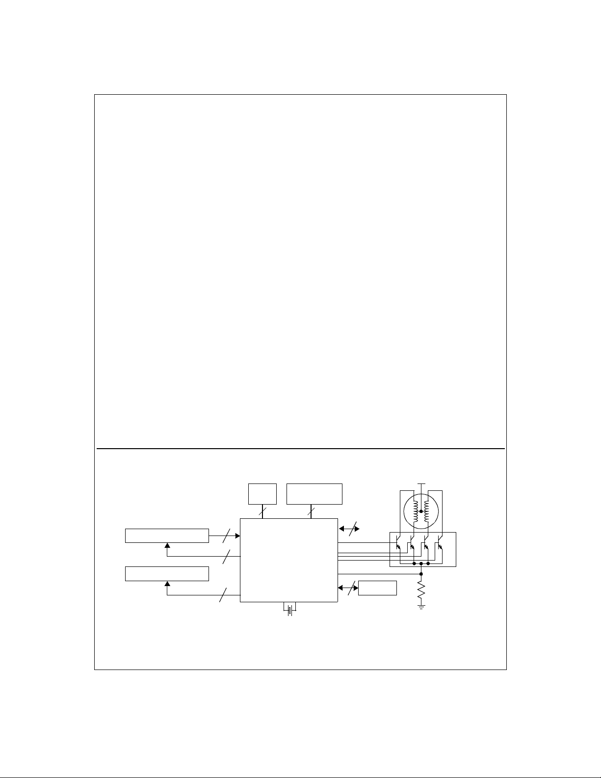
LM9831 Scanner System Block Diagram
USB
Port
2
2-6
1-3
1-3
LM9831CCVJD
CCD/CIS
Illumination
TRI-STATE® is a registered trademark of National Semiconductor Corporation.
©1999 National Semiconductor Corporation
Optional Serial
EEPROM
2
8MISC
I/O
30
DRAM
48MHz Crystal
1 www.national.com
+24V
Stepper
Motor
Power
Transistors
Page 2

Absolute Maximum Ratings (Notes 1 & 2) Operating Ratings (Notes 1 & 2)
Positive Supply Voltage (V+=VA=VD=V
With Respect to GND=AGND=DGND 6.5V
Voltage On Any Input or Output Pin -0.3V to V
Input Current at any pin (Note 3) ±25mA
Package Input Current (Note 3) ±50mA
Package Dissipation at T
ESD Susceptibility (Note 5)
= 25°C (Note 4)
A
Human Body Model 2000 V
Machine Model 250 V
Soldering Information
Infrared, 10 seconds (Note 6) 235°C
Storage Temperature -65°C to +150°
DRAM
)
+
+0.3V
Operating Temperature Range T
LM9831VJD 0°C≤TA≤+70°C
Supply Voltage +4.75V to +5.25V
V
A
V
Supply Voltage +4.75V to +5.25V
D
Supply Voltage +2.85V ≤ V
V
DRAM
|V
| ≤ 100mV
A-VD
Input Voltage Range -0.05V to V
Electrical Characteristics
The following specifications apply for AGND=DGND=0V, VA=VD=V
f
CRYSTAL IN
= 48MHz.
Boldface limits apply for T
A=TJ=TMIN
to T
Symbol Parameter Conditions
Full Channel Characteristics (in units of 12 bit LSBs unless otherwise noted)
Resolution with No Missing Codes 14 12 bits (min)
DNL Differential Non-Linearity V
INL Integral Non-Linearity Error (Note 11) V
Analog Channel Gain Constant
C
(ADC Codes/V), referred to 14 bits.
V
V
V
Pre-Boost Analog Channel Offset Error 26
OS1
Pre-PGA Analog Channel Offset Error -30
OS2
Post-PGA Analog Channel Offset Error -26
OS3
DRAM
DRAM
Includes voltage reference
variation, gain setting = 1
Coarse Color Balance PGA Characteristics (Configuration Registers 3B, 3C, and 3D)
Monotonicity
G
(Minimum PGA Gain) PGA Setting = 0 0.93
0
G
(Maximum PGA Gain) PGA Setting = 31 3.00
31
x3 Boost Gain
x3 Boost Setting On
(bit B5 of Gain Register is set)
Gain Error at any gain (Note 13) 0.3
Static Offset DAC Characteristics (Configuration Registers 38, 39, and 3A)
Monotonicity
Offset DAC LSB size PGA gain = 1 9
Offset DAC Adjustment Range PGA gain = 1 ±278
=+5.0VDC,
DRAM
; all other limits TA=TJ=25°C. (Notes 8, 9, & 10)
MAX
Typical
(Note 9)
=3.3V
=3.3V
-0.47
+0.95
-3.2
+2.6
8192
2.94
DRAM
Limits
(Note 10)
-1
+2.4
-12.6
+7.3
7412
9300
-34
+76
-80
+31
-75
+26
5
0.90
0.96
2.95
3.05
2.85
3.04
-0.6
+0.9
6
6
12
±256
MIN≤TA≤TMAX
≤ VD+100mV
+
+ 0.05V
Units
(Limits)
LSB (min)
LSB (max)
LSB (min)
LSB (max)
LSB (min)
LSB (max)
mV (min)
mV (max)
mV (min)
mV (max)
mV (min)
mV (max)
bits (min)
V/V (min)
V/V (max)
V/V (min)
V/V (max)
V/V (min)
V/V (max)
% (min)
% (max)
bits (min)
mV (min)
mV (max)
mV (min)
2 www.national.com
Page 3

Electrical Characteristics
The following specifications apply for AGND=DGND=0V, V
f
CRYSTAL IN
= 48MHz.
Boldface limits apply for T
(Continued)
A=TJ=TMIN
A=VD=VDRAM
to T
=+5.0VDC,
; all other limits TA=TJ=25°C. (Notes 8, 9, & 10)
MAX
Symbol Parameter Conditions
CCD/CIS Source Requirements for Full Specified Accuracy and Dynamic Range (Note 12)
V
CCDPEAK
Sensor’s Maximum Output Signal
Amplitude before LM9831 Analog Front
End Saturation
Gain = 0.933
Gain = 3. 0
Gain = 9.0
Analog Input C haracteristics
Average OS
OS
R
, OSG, OSB Input Current CDS Enabled, OS = 3.5V
R
, OSG, OSB Input Current CDS Disabled, OS = 3.5V
DC
DC
Internal Voltage Reference Characteristics
V
BANDGAP
V
REF LO
V
REF MID
V
REF HI
V
REGULA-
TOR
Voltage Reference Output Voltage 1.23 V
Negative Reference Output Voltage
Midpoint Reference Output Voltage
Positive Reference Output Voltage
USB I/O Voltage Regulator
DC and Logic Electrical Characteristics
The following specifications apply for AGND=DGND=0V, VA=VD=V
f
CRYSTAL IN
= 48MHz.
Boldface limits apply for T
A=TJ=TMIN
to T
Symbol Parameter Conditions
Digital Input Characteristics for D0-D15 (DRAM Interface)
V
V
V
C
Logical “1” Input Voltage
IN(1)
Logical “0” Input Voltage
IN(0)
I
Input Leakage Current ±0.1 µA
IN
Input Capacitance 5 pF
IN
V
V
V
DRAM
DRAM
DRAM
DRAM
Digital Input Characteristics for PAPER SENSE 1-2, MISC I/O 1-6, SDA, BUS POWER
CMODE
V
V
C
Logical “1” Input Voltage VD=5.25V
IN(1)
Logical “0” Input Voltage VD=4.75V
IN(0)
I
Input Leakage Current ±0.1 µA
IN
Input Capacitance 5 pF
IN
Digital Input Characteristics for D+, D-
V
V
C
Logical “1” Input Voltage VD=5.25V
IN(1)
Logical “0” Input Voltage VD=4.75V
IN(0)
I
Input Leakage Current ±0.1 µA
IN
Input Capacitance 5 pF
IN
=+5.0VDC unless otherwise noted,
DRAM
; all other limits TA=TJ=25°C. (Notes 8, 9, & 10)
MAX
=5.25V
=3.6V
=4.75V
=2.85V
, CRY STAL/EXT CLOCK, 24/48, RESET,
Typical
(Note 9)
Limits
(Note 10)
1.9
0.6
0.19
±3 nA
±26
-1.0 V
V
REF MID
/2.0 V
V
A
+1.0 V
V
REF MID
3.4
Typica l
(Note 9)
±30
Limits
(Note 10)
2.0
2.0
0.8
0.8
2.0
0.8
2.0
0.8
Units
(Limits)
V
V
V
µA (max)
V
Units
(Limits)
V (min)
V (min)
V (max)
V (max)
V (min)
V (max)
V (min)
V (max)
3 www.national.com
Page 4
DC and Logic Electrical Characteristics
The following specifications apply for AGND=DGND=0V, V
f
CRYSTAL IN
= 48MHz.
Boldface limits apply for T
A=TJ=TMIN
(Continued)
A=VD=VDRAM
to T
=+5.0VDC unless otherwise noted,
; all other limits TA=TJ=25°C. (Notes 8, 9, & 10)
MAX
Symbol Parameter Conditions
Digital Output Characteristics for D0-D15, A0-A9, RD
V
OUT(1)
V
OUT(0)
Digital Output Characteristics for A, B, A
V
OUT(1)
V
OUT(0)
Logical “1” Output Voltage
Logical “0” Output Voltage
, B
Logical “1” Output Voltage
Logical “0” Output Voltage
, WR, RAS, CAS (DRAM Interface)
V
V
V
V
V
V
V
V
DRAM
DRAM
DRAM
DRAM
DRAM
DRAM
DRAM
DRAM
=4.75V, I
=2.85V, I
=4.75V, I
=2.85V, I
=4.75V, I
=2.85V, I
=4.75V, I
=2.85V, I
OUT
OUT
OUT
OUT
OUT
OUT
OUT
OUT
=-4mA
=-4mA
=4mA
=4mA
=-10mA
=-10mA
=4mA
=4mA
Digital Output Characteristics for MISC I/O 1-6, TR1, TR2, ø1, ø2, RS, CP1, CP2, LAMP
V
V
OUT(1)
OUT(0)
Logical “1” Output Voltage VD=4.75V, I
Logical “0” Output Voltage VD=4.75V, I
OUT
OUT
=-4mA
=4mA
Digital Output Characteristics for D+, D-
V
V
OUT(1)
OUT(0)
Logical “1” Output Voltage VD=4.75V, I
Logical “0” Output Voltage VD=4.75V, I
OUT
OUT
=-1mA
=3mA
CRYSTAL IN, CRYSTAL OUT Characteristics
XTAL
XTAL
CRYSTAL OUT Bias Level (Offset) 0.8 V
OUT DC
CRYSTAL OUT Amplitude f
OUT AC
= 48MHz 0.8 V
CRYST AL
Power Supply Cha racteristics
I
I
I
DRAM
Analog Supply Current
A
(V
A
Digital Supply Current
D
(V
D
DRAM Supply Current
(V
DRAM
pins)
pins)
pins)
Operating
Suspend
Operating
Suspend (including I
Operating, V
Operating, V
Suspend
DRAM
DRAM
DRAM
= 5V
= 3V
)
Typica l
(Note 9)
, LAMPG, LAMP
R
87
1
37
14
10
5
14
Limits
(Note 10)
2.4
2.4
0.4
0.4
2.4
2.4
0.4
0.4
B
2.4
0.4
2.4
0.4
137
50
21
14
Units
(Limits)
V (min)
V (min)
V (max)
V (max)
V (min)
V (min)
V (max)
V (max)
V (min)
V (max)
V (min)
V (max)
P-P
mA (max)
µA (max)
mA (max)
µA (max)
mA (max)
mA (max)
µA (max)
4 www.national.com
Page 5
AC Electrical Ch ar acterist ic s
The following specifications apply for AGND=DGND=0V, VA=VD=V
f
CRYSTAL IN
C
= 48MHz, MCLK DIVIDER = 1.0 (unless otherwise noted), f
(databus loading) = 20pF/pin.
L
Boldface limits apply for T
A=TJ=TMIN
Symbol Parameter Conditions
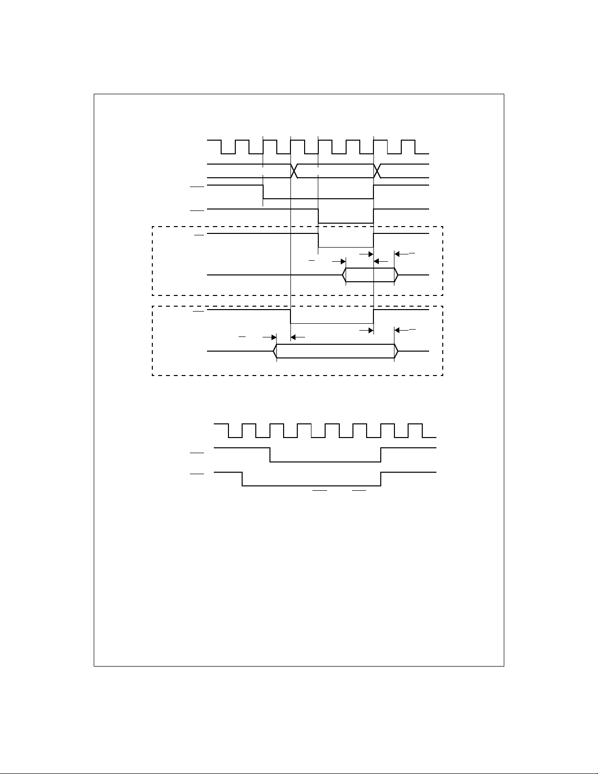
DRAM Timing (Figure 1)
V
=5.0V
t
RD SETUP
t
RD HOLD
t
WR SETUP
t
WR HOLD
Note 1:
Absolute Maximum Ratings indicat e limits beyond which damage to the device may occur. Operating Ratings indicat e conditions for which the device is functional,
but do not guarantee specific performance limits. For guaranteed speci fications and test conditions, see the Elec trical Characteristics. The guaranteed specifications apply
only for the test cond itions listed. Some performance characteristics may degrade when the device is not operated under the listed test conditions.
Note 2:
All voltages are measured with respect to GND=AGND=DGND =0V, unless otherwise specified.
Note 3:
When the input voltage (V
maximum package input current rating limits the number of pins that can simultaneously safely exceed the power supplies with an input c urrent of 25mA to two.
Note 4:
The maximum power dissipati on must be derated at elevated temperatures and is dictated by T
able power dissipation at any temperature is P
.
is 53°C/W
Note 5:
Human body model, 100pF capacitor discharged through a 1.5kΩ resistor. Machine model, 200pF capacitor discharged through a 0Ω resistor.
Note 6:
See AN-45 0 “Sur fa ce M oun tin g Met hod s a nd T hei r E ffect o n Pro duct Reliab ility” o r the sectio n titled “Su rfa ce Mount” found in any N ational Semiconductor Linear
Data Book for other methods of soldering surface mount devices.
Note 7:
Two diodes clamp the OS analog inputs to
impedance of the sensor, prevents damage to the LM9831 from transients during power-up.
Data valid to RD rising edge
Data valid after RD rising edge
Data valid before WR falling edge
Data valid after WR rising edge
) at any pin exceeds the power supplies (VIN<GND or VIN>VA or VD), the current at that pin should be limited to 25mA. The 50mA
IN
= (TJmax - TA) /
D
AGND
and VA as shown below. This input protection, in combination with the external clamp capacitor and the output
DRAM
V
=3.3V
DRAM
Θ
. TJmax = 150°C for this device. The typical thermal resistance (
JA
VA
=+5.0VDC unless otherwise noted,
DRAM
MCLK
to T
= f
CRYSTAL IN
MAX
/MCLK DIVIDER, f
; all other limits TA=TJ=25°C. (Notes 8, 9, & 10)
Typical
(Note 9)
Θ
max,
and the ambient temperature, TA. The maximum allow-
J
JA
= f
ADC CLK
Limits
(Note 10)
26
35
0
5
10
Θ
) of this part when board mounted
JA
Units
(Limits)
ns (min)
ns (min)
ns (min)
ns (min)
ns (min)
MCLK
/8,
OS Input
To Internal
Circuitry
AGND
Note 8:
For best performance, it is required that all supply pins be powered from the same power supply with separate bypass capaci tors at each supply pin.
Note 9:
Typicals are at T
Note 10:
Tested limits are guaranteed to National's AOQ L (Average Outgoing Quality Level).
Note 11:
Integr al linearity error is def ined as the devi ation of the analog value, expressed in LSBs, from the straight line that best fits the actual transfer function of the ADC.
Note 12:
V
is defined as the CCD OS voltage for the reference period following the reset feedthrough pulse. V
REF
a white (full scale) image with respect to the reference level, V
correctable range of pixel-to-pixel V
LM9831 can correct for using its internal PGA.
Note 13:
PGA Gain Error is the maximum difference between the measured gain for any PGA code and the ideal gain calculated by using the formula
V
--- -
PGA
V
G0X
Gain
=25°C, f
J=TA
WHITE
PGA code
--------------- ----------- -+=XG
where .
32
= 48MHz, and represent most likely parametric norm.
CRYSTAL IN
.
is defined as the peak positive deviation above V
V
REF
variation is defined as the maximum variation in V
–
()
31G0
RFT
V
RFT
V
32
----- -=
31
CCD Output Signal
V
REF
WHITE
is defined as the peak CCD pixel output voltage for
WHITE
of the reset feedthrough pulse. The maximum
(due to PRNU, light source intensity variation, optics, etc.) that the
WHITE
REF
5 www.national.com
Page 6
Timing Diagrams
48MHz Internal Clock
(t
= 20.83ns)
PERIOD
A0-A9 Row Address
RAS
CAS
RD
Read Operation
WR
Write Operation
01234560
n
Column Address
t
RD SETUP
n
Row Address
t
RD HOLD
n+1
DataD0-D15
t
t
WR SETUP
WR HOLD
DataD0-D15
Figure 1: DRAM Read and Write
48MHz Internal Clock
(t
= 20.83ns)
PERIOD
RAS
CAS
01234560
Figure 2: DRAM Refresh (CAS
before RAS)
6 www.national.com
Page 7
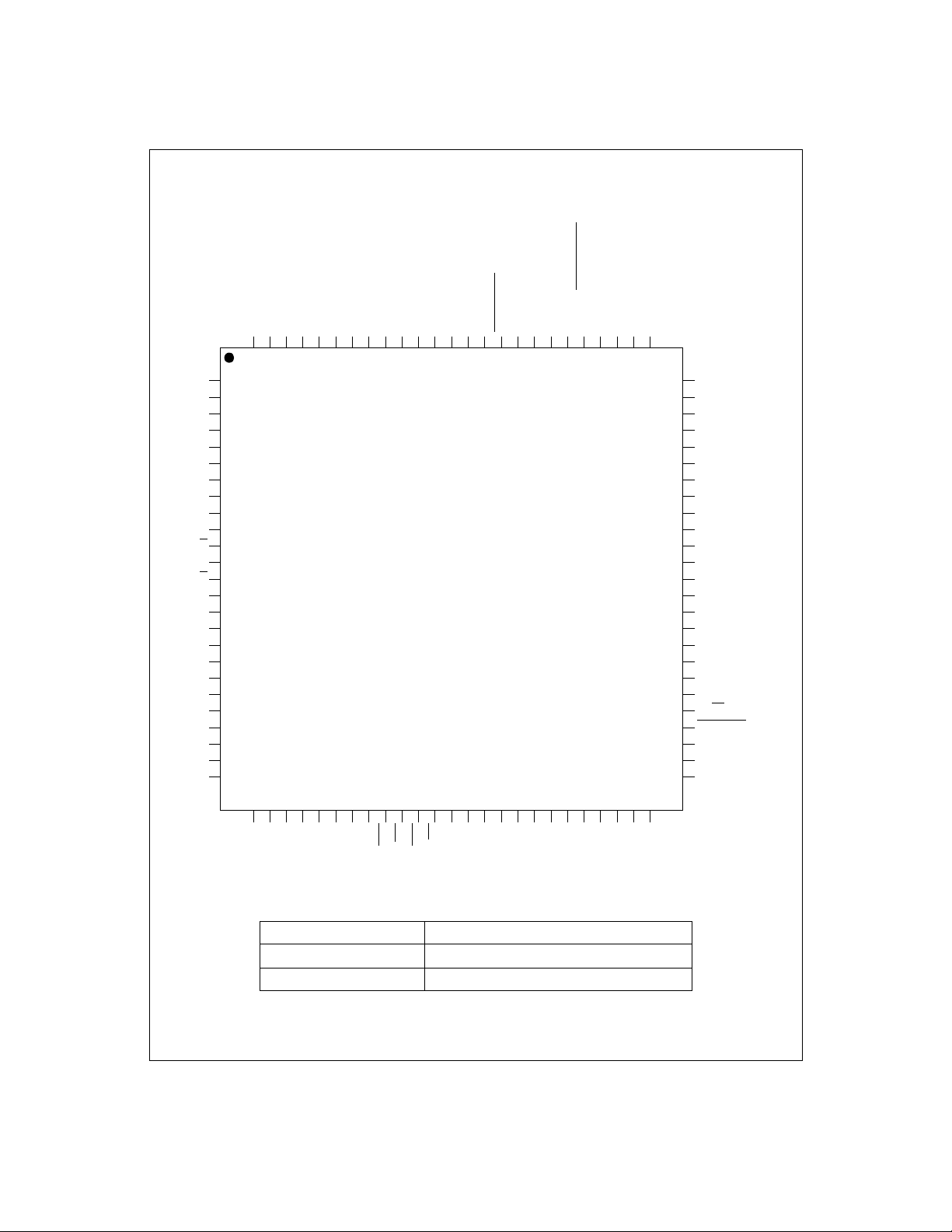
Connection Diagram
V
BANDGAP
V
REF LO
V
REF MID
V
REF HI
AGND
V
DGND
OS
OS
OS
V
D0
D15
DRAM
D1
D14
D2
D13
D3
D12
D4
D11
AGND VADGND VDTEST SENSEGND SENSEA SENSEB NC CMODE RESET NC NC DGND VDBUS POWR D+ D- V
10099 98 97 96 95 94 93 92 91 90 89 88 87 86 85 84 83 82 81 80 79 78 77 76
1
2
3
R
4
5
G
6
7
B
8
9
A
A
10
A
11
B
12
B
13
14
LM9831VJD
15
16
17
18
19
20
21
22
23
24
25
26 27 28 29 30 31 32 33 34 35 36 37 38 39 40 41 42 43 44 45 46 47 48 49 50
REGULATOR
DGND ACTIVE/SUSPENDED CP2 CP1 RS ø2
75
74
73
72
71
70
69
68
67
66
65
64
63
62
61
60
59
58
57
56
55
54
53
52
51
ø1
TR2
TR1
MISC I/O 6
MISC I/O 5
MISC I/O 4
DGND
V
MISC I/O 3
MISC I/O 2
MISC I/O 1
D
PAPER SENSE 1
PAPER SENSE 2
V
D
DGND
LAMP
B
LAMP
G
LAMP
R
DGND
V
D
24/48
CRYSTAL
CRYSTAL IN
/EXT
CRYSTAL OUT
SCL
CLK
D5
D6
D9
D10
Ordering Information
Commercial (0°C ≤ TA ≤ +70°C) Package
LM9831CCVJD VJD100A 100 Pin Thin Quad Flatpac
LM9831CCVJDX VJD100A 100 Pin Thin Quad Flatpac, Tape and Reel
D7
D8
WR
DRAM
DGND
V
CAS
A9A8A0A7A1
RD
RAS
A6A2A5A3A4
DRAM
DGND
V
SDA
7 www.national.com
Page 8
Pin Descriptions
g
USB Interface
D+, D- Digital I/O. USB Interface signals
BUS POWER
ACTIVE/
SUSPENDED
SDA Digital I/O. Serial Data to/from external
SCL Digital Output. Serial Clock Output to external
Digital Input. Tie low for bus powered systems, tie high for external power.
Digital Output. Low in Suspend mode. High in
operational mode. Used to control external
regulators, other components.
EEPROM.
EEPROM.
Analo
OSR,
OS
,
G
OS
B
V
REF LO
V
REF MID
V
REF HI
V
BANDGAP
V
REGULATOR
Analog Inputs. These i nputs (for Red, Green,
and Blue) should be tied to the sensor’s output signal th rough DC blocking capacitors. If
unused, tie to ground through DC blocking
capacitors.
Analog Output/Input. Bypass to AGND with a
0.047µF monolithic capacitor. Do not put a
DC load on this pin.
Analog Output/Input. Bypass to AGND with a
0.047µF monolithic capacitor. Do not put a
DC load on this pin.
Analog Output/Input. Bypass to AGND with a
0.047µF monolithic capacitor. Do not put a
DC load on this pin.
Analog Output. Bypass to AGND with a
0.047µF monolithic capacitor. Do not put a
DC load on this pin.
Analog Output. Bypass to AGND with a
0.047µF monolithi c capacitor. Used as terminal voltage for 1.5k D+ pullup resistor.
DRAM
D0 (LSB) -D15
(MSB)
RD
WR
A0-A9 Di gital Outputs. Address pins for up to 1M x
RAS
CAS
Digital Inputs/Outputs. This is the 16 bit data
path between the external DRAM and the
LM9831.
Digital Output. Read signal to external DRAM.
Digital Output. Write signal to external DRAM.
16 external DRAM.
Digital Output. Row Address Strobe signal.
Digital Output. Column Address Strobe sig-
nal.
Scanner Support I/O
PAPER
SENSE 1-2
MISC I/O 1-6 Digital Inputs/Outputs. Programmable, used
Digital Inputs. Programm able, used for sensing home position, paper, front panel
switches, etc.
for front panel switches, status LE Ds, etc. At
power-on and in Suspend Mode, MISC I/Os
1-3 are inputs and MISC I/Os 4-6 are outputs.
Stepper Motor
A, B, A, B Digital Outputs. Pulses to stepper motor drive
SENSE
A
SENSE
B
SENSE
GND
circuitry.
,
Analog Inputs. Current sensing for stepper
motor’s PWM current co ntrol.
Analog Input. G round se nse input for s tepper
motor’s PWM current co ntrol.
Sensor Control
ø1 Digital Output. CCD/CIS clock signal phase 1.
ø2 Digital Output. CCD/CIS clock signal phase 2.
RS Digital Output. Reset pulse for the CCD/CIS.
CP1 Digital Output. Clamp pulse for the CCD/CIS.
CP2 Digital Output. Clamp pulse for the CCD/CIS.
TR1, TR2 Digital Outputs. Transfer pulses for the
,
LAMP
R
LAMP
,
G
LAMP
B
CCD/CIS.
Digital Output s. Used to cont rol R, G, and B
LEDs of single output CIS, as wel l as brightness of CCFL. The CDS signal can b e seen
on LAMP
7).
in a test mode (see register 5E, bit
B
Master Clock Generation
CRYSTAL IN Digital Input. Used with CRYSTAL OUT and
CRYSTAL
OUT
CRYSTAL
EXT CL OCK
24/48
an external 48MHz crystal to form a crystal
oscillator.
Digital Output. Used with CRYSTAL IN and an
external 48MHz crystal to form a crystal oscillator.
/
Digital Input. Tie to DGND for operation wi th
an external crystal. Pull up to V
CRYSTAL OUT with an external TTL or
CMOS clock source.
Digital Input. Tie to DGND for operation with a
48MHz crystal or external clock. Pull up to V
for operation with a 24MHz crystal or external
clock. NOTE: Operation at 24MHz is not guaranteed - always use a 48MHz crystal.
to drive
D
D
8 www.national.com
Page 9

Miscellaneous
RESET Digital input. Ta ke high to force device into
TEST Analog Output.
CMODE Digital Input. Test mode, always tie high.
Power On Reset state, low to exit reset state.
Analog Power Supplies (4 pins)
VA (2) This is the positive supply pin for the analog
AGND (2) This is the ground r eturn for the analog sup -
supply. It should be connected to a v oltage
source of +5V and bypassed to AGND with a
0.1µF monolithic capacitor in parallel with a
10µF tantalum capacitor.
ply.
Digital Power Supplies (17 pins)
VD (5) This is the positive supply pin for the digital
(3) This is the po sitive supply pi n for the digital
V
DRAM
DGND (9) This is the ground return for V
supply. It should be connected to a v oltage
source of +5V and by passed to D GND wi th a
0.1µF monolithic capacitor.
supply for the LM9831’s external DRAM I/O. It
also powers the A, B, A
outputs. It should be connected to a 3 or 5V
supply and bypassed to the closest DGND pin
with a 0.1µF monolithic capacitor.
, and B stepper motor
and V
D
DRAM
.
9 www.national.com
Page 10
LM9831 Register Listing
Registers in bold boxes are reset to that value on power-up. All register addresses are in hexadecimal. All other numbers are
decimal unless otherwise noted.
Address Function
IMAGE BUFFER (READ ONLY)
00
Pixel (Image) D ata
STATUS REGISTERS (READ ONLY)
01
Image Data Available In Buffer
PAPER SENSE 1 State
read clears bit if edge sensitive input.
PAPER SENSE 2 State
read clears bit if edge sensitive input.
MISC I/O 1 State
read clears bit if edge sensitive input.
MISC I/O 2 State
read clears bit if edge sensitive input.
02
MISC I/O 3 State
read clears bit if edge sensitive input.
MISC I/O 4 State
read clears bit if edge sensitive input.
MISC I/O 5 State
read clears bit if edge sensitive input.
MISC I/O 6 State
read clears bit if edge sensitive input.
DATAPORT REGISTERS
DataPort Target
DataPort Targ et Color
03
Pause (Read Only)
This bit indicates whether or not the scanner
is currently paused due to a buffer full
condition.
DRAM Test
04
DataPort Address - MSB
05
DataPort Address - LSB
06
nnnnnnnn
DataPort
D7D6D5D4D3D2D1D
n n n n n n n n One byte of image data.
nnnnnnnn
0False
1True
0False
1True
0False
1True
0False
1True
0 Normal State
1 The scanner is currently in the pause/reverse cycle.
0 Normal Operation
1 DRAM Test mode
R
/Waaaaaa
aaaaaaaa
0
n*2 (256k x 16 DRAM) or n*8 (1M x 16 DRAM)
kilobytes of image data is available
0False
1True
0False
1True
0False
1True
0False
1True
0 0 Offset Coefficient Data
0 1 Gain Coefficient Data
1 0 Gamma Lookup Table
11N/A
00 Red
0 1 Green
10 Blue
11 N/A
Address of location to be read/written to.
a = 0 to 4095 for gamma tables,
0 to 16383 for Offset and Gain Coefficient Data
Addresses greater than these are illegal.
Bit D6 of register 4 indicates whether next operation
will be a Read (D6=1) or a Write (D6=0)
Data to be read from or written to the address of the
currently selected Dataport Target. The DataPort
Address is automatically incremented whenever one
(gamma data) or two (Gain/Offset Data) bytes are
read from or written to this register.
Value
.
10 www.national.com
Page 11
Address Function
COMMAND REGISTER
Command Register
This register is used to start and end a scan.
It is also used to home the sensor in a
flatbed scanner or eject the image in a
sheetfed scanner.
Note: Always make sure
the Command Register is in the idle state
(=0) before issuing a new command.
07
Standby
When this bit is set the entire chip enters a
low power state.
Warning: A Standby command will stop
DRAM refresh.
Reset
Write a 1 then a 0 to reset the LM9831’s
state machines.
Warning: A Reset will stop DRAM refresh.
MASTER CLOCK DIVIDER
MCLK Divider
This register sets the master clock frequency
for the entire scanner.
08
f
= 48MHz/MCLK_Divider
MCLK
f
= f
MCLK
/8
ADC
D7D6D5D4D3D2D1D
0
Idle - Stops motor (A, B, A
000
completes current line of data (if scanning).
Note: CCD/CIS clocks continue clocking.
High Speed Forward - Moves motor forward at a
001
speed determined by the Fast Feed Step Size
(registers 48 and 49).
High Speed Reverse - Moves motor backward at a
010
speed determined by the Fast Feed Step Size
(registers 48 and 49).
Start Scan - Resets the LM9831’s data pointers and
011
starts an image scan.
Programmed High Speed Forward - Moves motor
forward at a speed determined by the Fast Feed Step
101
Size (registers 48 and 49) for the number of lines
programmed in registers 4A and 4B.
Programmed High Speed Reverse - Moves motor
backward at a speed determined by the Fast Feed
110
Step Size (registers 48 and 49) for the number of lines
programmed in registers 4A and 4B.
0 Normal Operation
1 Low Power Standby Mode
0 Normal Operation
1 Resets the LM9831
000000÷1.0
000001÷1.5
000110÷4
a a a a a a ÷ ((aaaaaa/2)+1)
111110÷32.0
111111÷32.5
Value
, B = 0),
11 www.national.com
Page 12
Address Function
HORIZONTAL RESOLUTION AND DA TAMODE SETTINGS
Horizontal DPI Divider
This register determines the horizontal
resolution of the scan.
Scan resolution = Optical resolution divided
by the Horizontal_DPI_Divider.
Pixel Packing
This register determines how many bits in
09
each byte of data are transmitted to the host
when DataMode = 0
DataMode
When DataMode = 0, the pixel data is fully
processed, going through the Offset,
Shading, Horizontal DPI Adjust, Gamma,
and Pixel Packing blocks.
When DataMode = 1, 14 bit data is extracted
following the Shading Multiplier stage.
Gamma and any other post processing must
be done by the host.
RESERVED
0A Reserved 0 0 0 0 0 0 0 0 Write 00 to this register
SENSOR CONFIGURATION
Input Signal Polarity
CDS On/Off
Standard/Even-Odd Senso r
0B
CIS TR1 Timing Mode
Fake Optical Black Pixels
(for Dyna-type CIS sensors)
D7D6D5D4D3D2D1D
0 0 1 bit/pixel (1 bit grayscale/3 bit color)
0 1 2 bits/pixel (2 bit grayscale/6 bit color)
1 0 4 bits/pixel (4 bit grayscale/12 bit color)
1 1 8 bits/pixel (8 bit grayscale/24 bit color)
0
1
0 0 Off - use standard CCD Timing
01
10
11 N/A
0 Off: Normal operation
1 On: RS pulse held high for entire Optical Black period
0
000÷1
001÷1.5
010÷2
011÷3
100÷4
101÷6
110÷8
111÷12
1, 2, 4, or 8 bit image data,
as determined by the Pixel Size setting.
14 bit image data - sent in 2 bytes, MSB first:
First Byte: 13 12 11 10 09 08 07 06
Second Byte: 05 04 03 02 01 00 XX XX
(XX: bits set to 0)
0 Negative (Most CCD Sensors and Toshiba CIS)
1 Positive (Most CIS Sensors)
0 CDS Off
1 CDS On
0 Standard (1 pixels per Ø period)
1 Even/Odd (2 pixels per Ø period)
CIS TR1 Timing Mode 1:
TR1 pulse = exactly one Ø clock,
starting at rising edge of Ø1
CIS TR1 Timing Mode 2:
TR1 pulse = exactly one Ø clock,
TR1 centered around Ø1 high.
Value
12 www.national.com
Page 13
Address Function
SENSOR CONTROL SETTINGS
Ø1 Polarity
Ø2 Polarity
RS Polarity
0C
CP1 Polarity
CP2 Polarity
TR1 Polarity
TR2 Polarity
Ø1 Active/Off
Ø2 Active/Off
RS Active/Off
CP1 Active/Off
0D
CP2 Active/Off
TR1 Active/Off
TR2 Active/Off
Number of TR Pulses
TR Pulse Duration
0E
TR-Ø1 Guardband Duration
0F
Optical Black Clamp Start
10
Optical Black Clamp End
11
Rese t Pulse Start
12
Reset Pulse Stop
13
CP1 Pulse Start
14
CP1 Pulse Stop
15
CP2 Pulse Start
16
CP2 Pulse Stop
17
Reference Sample Position
18
Signal Sample Position
INTEGRATION TIME ADJUST
19
Integration Time Adjustment Function
STEPPER PHASE CORRECTION
1A
TR to Stepper Phase Correction - MSB
1B
TR to Stepper Phase Correctio n - LSB
D7D6D5D4D3D2D1D
0
Value
0Positive
1 Negative
0Positive
1 Negative
0Positive
1 Negative
0Positive
1 Negative
0Positive
1 Negative
0Positive
1 Negative
0Positive
1 Negative
0Off
1Active
0Off
1Active
0Off
1Active
0Off
1Active
0Off
1Active
0Off
1Active
0Off
1Active
01 TR Pulse
12 TR Pulses
n n n n n+1 pixel periods (1-16)
n n n n n pixel periods (0-15)
nnnnn
nnnnn
nnnnn
nnnnn
nnnnn
nnnnn
nnnnn
nnnnn
nnnnn
nnnnn
nnnnnnnt
pixel rate: n=0-23, line rate: n=0-7 MCLKs from Ø1 edge
pixel rate: n=0-23, line rate: n=0-7 MCLKs from Ø1 edge
pixel rate: n=0-23, line rate: n=0-7 MCLKs from Ø1 edge
pixel rate: n=0-23, line rate: n=0-7 MCLKs from Ø1 edge
pixel rate: n=0-23, line rate: n=0-7 MCLKs from Ø1 edge
pixel rate: n=0-23, line rate: n=0-7 MCLKs from Ø1 edge
pixel rate: n=0-23, line rate: n=0-7 MCLKs from Ø1 edge
pixel rate: n=0-23, line rate: n=0-7 MCLKs from Ø1 edge
pixel rate: n=0-23, line rate: n=0-7 MCLKs from Ø1 edge
pixel rate: n=0-23, line rate: n=0-7 MCLKs from Ø1 edge
= n*t
READOUT
, n = 1 to 127. n=0 turns off function.
INT
First step of scan occurs n pixels (1 - 16383) after first
nnnnnn
TR pulse. This register can be used to set the phase
between the TR pulses and the stepper motor pulses.
NOTE: a setting of n = 0 creates the maximum delay
nnnnnnnn
(16384) pixels, which will increase scan time. If this
function is not used, this register should be set to 1.
13 www.national.com
Page 14

Address Function
D7D6D5D4D3D2D1D
0
SENSOR PIXEL CONFIGURATION
1C
Optical Black Pixels Start
1D
Optical Black Pixels End
1E
Active Pixels Start - MSB
1F
Active Pixels Start - LSB
20
Line End - MSB
21
Line End - LSB
n n n n n n n n n pixels (0 - 255)
n n n n n n n n n pixels (0 - 255)
n n n n n n n pixels (0 - 16383)
nnnnnnnn
nnnnnn
nnnnnnnn
Set to the same value as register
n pixels (0 - 16383)
This selects the pixel count at which the current line is
ended and the next line begins. This determines the
integration time of one line.
PIXEL DATA RANGE TO PROCESS
n pixels (
22
Data Pixels S tart - MSB
nnnnnn
Active Pixels Start
This selects the start of the range of pixels transmitted
to the PC and determines the pixel location where
23
Data Pixels S tart - LSB
nnnnnnnn
offset and shading correction begins (pixel 0 in the
DataPort). This value must be >=
24
Data Pixels End - MSB
25
Data Pixels End - LSB
nnnnnnn pixels (
nnnnnnnn
Data Pixels Start
This selects the end of the range of pixels transmitted
to the PC. This value must be <= [
COLOR MODE SETTINGS
0 0 0 3 Channel Pixel Rate Color
AFE Operation
3 Channel or 1 Channel
0 0 1 3 Channel Line Rate Color
1 0 0 1 Channel Grayscale
1 0 1 1 Channel Color
1 Channel Grayscale Input Source
(1 Channel Color always uses the
26
Blue Channel as the input)
TR
(=TR1) position
RED
(3 Channel Line Rate Mode only)
TR
(=TR2) position
GREEN
(3 Channel Line Rate Mode only)
TR
(=CP2) position
BLUE
(3 Channel Line Rate Mode only)
0 0 Red Channel
0 1 Green Channel
1 0 B lue Channe l
11 N/A
0 1st TR pulse position (inside Ø1 high)
1 2nd TR pulse position (inside Ø1 low)
0 1st TR pulse position (inside Ø1 high)
1 2nd TR pulse position (inside Ø1 low)
0 1st TR pulse position (inside Ø1 high)
1 2nd TR pulse position (inside Ø1 low)
0 0 Do not drop any TR
3 Channel Line R ate TR
(3 Channel Line Rate Mode only)
RED
drop
0 1 Drop 1 TR
1 0 Drop 2 TR
11N/A
RED
RED
0 0 Do not drop any TR
3 Channel Line R ate TR
(3 Channel Line Rate Mode only)
27
GREEN
drop
0 1 Drop 1 TR
1 0 Drop 2 TR
11 N/A
GREEN
GREEN
0 0 Do not drop any TR
3 Channel Line R ate TR
(3 Channel Line Rate Mode only)
BLUE
drop
Triple TR output
0 1 Drop 1 TR
1 0 Drop 2 TR
11 N/A
BLUE
BLUE
0 Normal operation
1 Outputs single TR pulse on TR1, TR2, and CP2 pins
RESERVED
28 Reserved 0 0 0 0 0 0 0 0 Write 00 to this register
Value
Data Pixels Start
- 16383)
Active Pixels Start
- [
Line End
- 20])
Line End
pulses
RED
pulse (double integration time)
pulses (triple integration time)
pulses
GREEN
pulse (double integration time)
pulses (triple integration time)
pulses
BLUE
pulse (double integration time)
pulses (triple integration time)
.
- 20]
14 www.national.com
Page 15

Address Function
D7D6D5D4D3D2D1D
ILLUMINATION SETTINGS
Illumination Mode
Controls the function of the 3 LAMP outputs:
, LAMPG, and LAMP
LAMP
R
B
Mode 0 is the Off/Reset state.
Mode 1 is typically used for CCFL lamps.
29
Mode 2 is for color scanning with tri-color
LEDs.
Mode 3 is for grayscale scanning with tricolor LEDs.
2A
2C
2D
2E
2F
30
31
32
33
34
35
36
37
LAMP
LAMP
LAMP
LAMP
LAMP
LAMP
LAMP
LAMP
LAMP
LAMP
LAMP
LAMP
LAMP
LAMP
PWM - MSB
G
PWM - LSB
G
On - MSB
R
On - LSB
R
Off - MSB
R
Off - LSB
R
On - MSB
G
On - LSB
G
Off - MSB
G
Off - LSB
G
On - MSB
B
On - LSB
B
Off - MSB
B
Off - LSB
B
(Illumination Mode 1) n n n n LAMP
(Illumination Mode 1) n n n n n n n n
n n n n n n n pixels (1 - 16384)
nnnnnnnn
n n n n n n n pixels (1 - 16384)
nnnnnnnn
n n n n n n n pixels (1 - 16384)
nnnnnnnn
n n n n n n n pixels (1 - 16384)
nnnnnnnn
n n n n n n n pixels (1 - 16384)
nnnnnnnn
n n n n n n n pixels (1 - 16384)
nnnnnnnn
STATIC OFFSET AND GAIN SETTINGS FOR ANALOG FRONT END
38
Static Offset (Red)
39
Static Offset (Green)
3A
Static Offset (Blue)
3B
Static Gain (Red)
3C
Static Gain (Green)
3D
Static Gain (Blue)
0 n n n n n Offset = +n*9.3mV, n = 0 to 31
1 n n n n n Offset = -n*9.3mV, n = 0 to 31
0 n n n n n Offset = +n*9.3mV, n = 0 to 31
1 n n n n n Offset = -n*9.3mV, n = 0 to 31
0 n n n n n Offset = +n*9.3mV, n = 0 to 31
1 n n n n n Offset = -n*9.3mV, n = 0 to 31
0 n n n n n Gain = 0.93 + 0.067*n (V/V), n = 0 to 31
1 n n n n n Gain = 3(0.93 + 0.067*n) (V/V), n = 0 to 31
0 n n n n n Gain = 0.93 + 0.067*n (V/V), n = 0 to 31
1 n n n n n Gain = 3(0.93 + 0.067*n) (V/V), n = 0 to 31
0 n n n n n Gain = 0.93 + 0.067*n (V/V), n = 0 to 31
1 n n n n n Gain = 3(0.93 + 0.067*n) (V/V), n = 0 to 31
0
= LAMPG = LAMPB = 0V
LAMP
00
R
(Power-On/Reset Default)
Illuminati on Mode 1 - LAMP
every line, with their on and off points controlled by
the Pixel Counter settings. LAMP
continuous PWM pulse stream. (Figure 20)
01
LAMP
and/or LAMPB may be set to stay on or off at
R
all times by setting the LAMP Off or LAMP On settings
Value
and LAMPB turn on
R
Output is
G
(registers 2C-37) greater than the Line End value
(registers 20 and 21).
Illumination Mode 2 - LAMP
sequentially at the line rate, with their on and off
10
points controlled by Pixel Counter settings. (Figure
, LAMPG, LAMPB turn on
R
21)
Illumination Mode 3 - LAMP
11
every line, with their on and off points controlled by
, LAMPG, LAMPB turn on
R
the Pixel Counter settings. (Figures 22 and 23)
output is a PWM pulse stream. Duty cycle is
G
n/4095. Frequency = 48Mhz/4096 = 11.7kHz2B
This selects the pixel count at which the LAMP
output goes high (if programmed)
This selects the pixel count at which the LAMP
output goes low (if programmed)
This selects the pixel count at which the LAMP
output goes high (if programmed)
This selects the pixel count at which the LAMP
output goes low (if programmed)
This selects the pixel count at which the LAMP
output goes high (if programmed)
This selects the pixel count at which the LAMP
output goes low (if programmed)
R
R
G
G
B
B
15 www.national.com
Page 16

Address Function
DIGITAL PIXEL RATE OFFSET AND GAIN SETTINGS
3E
Fixed Offset Coefficient - MSB
3F
Fixed Offset Coefficient - LSB
40
Fixed Multiplier Coefficient - MSB
41
Fixed Multiplier Coefficient - LSB
DIGITAL PIXEL RATE OFFSET AND GAIN/DRAM SETTINGS
Shading Multiplier
Multiplier Coefficient Source
42
Offset Coefficient Source
Reserved
DRAM Size
D7D6D5D4D3D2D1D
nnnnnnnn
nnnnnn00
nnnnnnnn
nnnnnnnn
0
Fixed Offset to use for calibration
Fixed Gain to use for calibration
0 Gain = [Multiplier Coefficent]/16384
1 Bypass Multiplier
0 Configuration Register 40 and 41 (Fixed)
1 External DRAM
0 Configuration Register 3E and 3F (Fixed)
1 External DRAM
1 0 Set to 10
0 256k x 16
11M x 16
Value
16 www.national.com
Page 17

Address Function
STEPPER MOTOR CONTROL SETTINGS
n (Line Skipping)
43
Part of the “n out of m” function, consisting of
registers 43, 44, and 54 (bits 3-7).
m (Line Skipping)
44
Part of the “n out of m” function, consisting of
registers 43, 44, and 54 (bits 3-7).
Full/Microstepping
Current Sensing Phases
= 0 for fullstepping
= 1 fo r microstepping
Stepper Motor Phase A Polarity
45
Stepper Motor Phase B Polarity
A, B, A
, and B stepper motor status
46
Scanning Step Size - MSB
Scanning Step Size - LSB
48
Fast Feed Step Size - MSB
Fast Feed Step Size - LSB
4A
Fullsteps to Skip at Start of Scan - MSB
Fullsteps to Skip at Start of Scan - LSB
Fullsteps to Scan after PAPER SENSE 2
4C
trips -MSB
Fullsteps to Scan after PAPER SENSE 2
trips -LSB
4E
Pause scanning, stop/reverse motor
4F
Resume scanning, start motor
50
Full steps to reverse when buffer is full
Accelerati on Profile (stopped)
Acceleration Profile (25%)
51
Acceleration Profile (50%)
Default Phase Difference - High Byte
52
Default Phase Difference - Mid Byte
53
Default Phase Difference - Low Byte
Lines to Process After Pause/
Lines to Discard after Resume
Line Skipping Phase
Part of the “n out of m” function, consisting of
54
registers 43, 44, and 54 (bits 3-7).
Line Skipping Color Phase Delay
Part of the “n out of m” function, consisting of
registers 43, 44, and 54 (bits 3-7).
Kickstart steps
55
Hold Current Timeout
56
Stepper Motor PWM Frequency
57
Stepper Motor PWM Set Duty Cycle
(fullstepping mode) n n n Motor gets maximum current for first n (0-7) full steps
D7D6D5D4D3D2D1D
tttttttt
mmmmmmmm
0
1A, B, A
n n n n n n n n The step size of one microstep while scanning, in
nnnnnnnn
n n n n n n The step size of one microstep while fast feeding, in
nnnnnnnn
n n n n n n n When scan starts, paper is fed forward n full steps (0 -
nnnnnnnn
nnnnnnnn
nnnnnnnn
nnnnnnnn
n n n n n n n (0-63) full steps (0 = do not reverse)
n n n (0-3) full steps at 25% speed
n n n (0-3) full steps at 50% speed
nnnnnnnn
nnnnnnnn
n n n n n lines, n = 0-15
n n n n n Full step time units (1-31) (do not set to 0)
nnnnnnnn
n n n n n n = minimum of n/64 (default = 0)
17 www.national.com
0
n lines saved in DRAM for every m lines (register 44)
scanned, function bypassed if register value = 0.
n (lines saved per m lines scanned) = 256 - t
t = 256 - n
If t = 0 then function is bypassed.
n lines (register 43) saved in DRAM for every m lines
scanned. m = 1 to 255.
If m = 0 then function is bypassed.
0 Full Step Mode
1 Microstepping Mode
1 Phase - No microstepping, just kickstart/stop
0
functions
1 2 Phases - necessary for microstepping
0
Positive (A/B/A
Negative (A/B/A
WARNING: When idle, this setting leaves the motor
1
energized for unipolar motors, and will destroy bipolar
motor drivers. Keep this bit set to a 0.
0
1
n n n n Adds a delay of n (0-4095) full steps between when
n n n (0-3) full step time units pause while stopped
0 Red sensor data arrives before Green sensor
1 Blue sensor data arrives before Green sensor
Positive (A/B/A
Negative (A/B/A
WARNING: When idle, this setting leaves the motor
energized for unipolar motors, and will destroy bipolar
motor drivers. Keep this bit set to a 0.
A, B, A
, and B output pins in Tri-State
, and B output pins active
units of pixel periods (minimum 2)47
units of pixel periods (minimum 2)49
32767) at highest speed. For “zooming” in flatbeds4B
PAPER SENSE 2 trips and when the scanning bit is
reset, terminating the scan/motor movement4D
Pause scan when buffer is n*2 (16 x 256k) or
n*8 (16x1M) kbytes full
Resume scan when buffer is n*2 (16 x 256k) or
n*8 (16x1M) kbytes full
n n 18 bit word used to calculate when motor resumes
after reversing and stopping. 1 < n < 262143. 2 bits in
register 51 are the most significant bits of 18 bit word.
n (0-7) lines. This only applies if the motor doesn’t
nnn
reverse (reverse steps = 0)
=CRYSTAL OUT/(256*n) (0 < n < 256)
=CRYSTAL OUT/(256*256) (n = 0)
Value
/B Output high = winding energized)
/B output low = winding energized)
/B Output high = winding energized)
/B output low = winding energized)
Page 18

Address Function
PAPER SENSE SETTINGS
PAPER SENSE 1: Polarity
PAPER SENSE 1: Level/Edge sensitive
PAPER SENSE 1: Stop Scan
58
PAPER SENSE 2: Polarity
PAPER SENSE 2: Level/Edge sensitive
PAPER SENSE 2: Stop Scan
MISC I/O PIN SETTINGS
MISC I/O 1: Input or Output
MISC I/O 1: Polarity
(if configured as an input)
MISC I/O 1: Level/Edge sensitive
(if configured as an input)
MISC I/O 1: Output State
(if configured as an output)
Power On/USB Suspend Default: Input
59
MISC I/O 2: Input or Output
MISC I/O 2: Polarity
(if configured as an input)
MISC I/O 2: Level/Edge sensitive
(if configured as an input)
MISC I/O 2: Output State
(if configured as an output)
Power On/USB Suspend Default: Input
D7D6D5D4D3D2D1D
0
1
0
1
0 The MISC I/O 2 pin is configured as an input.
1 The MISC I/O 2 pin is configured as an output.
0 A low input on MISC I/O 2 is True
1 A high input on MISC I/O 2 is True
0
1
0
1
0
0 A low input on PAPER SENSE 1 is True
1 A high input on PAPER SENSE 1 is True
Level sensitive: PAPER SENSE 1 State bit (in Status
0
Register) is set to a 1 if PAPER SENSE 1 is currently
True.
Edge sensitive: PAPER SENSE 1 State bit (in Status
1
Register) is set to a 1 if PAPER SENSE 1 has been
True since the last time the Status Register was read.
Transitions on PAPER SENSE 1 will not clear the
0
scanning bit.
A False - to - True transition on PAPER SENSE 1 will
1
0 A low input on PAPER SENSE 2 is True
1 A high input on PAPER SENSE 2 is True
0
1
clear the Command Register and stop the scan.
Level sensitive: PAPER SENSE 2 State bit (in Status
Register) is set to a 1 if PAPER SENSE 2 is currently
True.
Edge sensitive: PAPER SENSE 2 State bit (in Status
Register) is set to a 1 if PAPER SENSE 2 has been
True since the last time the Status Register was read.
Transitions on PAPER SENSE 2 will not clear the
scanning bit.
A False - to - True transition on PAPER SENSE 2 will
clear the Command Register and stop the scan (after
the number of lines specified in the
after PAPER SENSE 2 trips
0 The MISC I/O 1 pin is configured as an input.
1 The MISC I/O 1 pin is configured as an output.
0 A low input on MISC I/O 1 is True
1 A high input on MISC I/O 1 is True
Level sensitive: MISC I/O 1 State bit (in Status
0
Register) is set to a 1 if MISC I/O 1 is currently True.
Edge sensitive: MISC I/O 1 State bit (in Status
1
Register) is set to a 1 if MISC I/O 1 has been True
since the last time the Status Register was read.
The output of the MISC I/O 1 pin will be a logic low
(0V).
The output of the MISC I/O 1 pin will be a logic high
(5V).
Level sensitive: MISC I/O 2 State bit (in Status
Register) is set to a 1 if MISC I/O 2 is currently True.
Edge sensitive: MISC I/O 2 State bit (in Status
Register) is set to a 1 if MISC I/O 2 has been True
since the last time the Status Register was read.
The output of the MISC I/O 2 pin will be a logic low
(0V).
The output of the MISC I/O 2 pin will be a logic high
(5V).
Value
Lines to Scan
register).
18 www.national.com
Page 19

Address Function
MISC I/O 3: Input or Output
MISC I/O 3: Polarity
(if configured as an input)
MISC I/O 3: Level/Edge sensitive
(if configured as an input)
MISC I/O 3: Output State
(if configured as an output)
Power On/USB Suspend Default: Input
5A
(NEW)
MISC I/O 4: Input or Output
MISC I/O 4: Polarity
(if configured as an input)
MISC I/O 4: Level/Edge sensitive
(if configured as an input)
MISC I/O 4: Output State
(if configured as an output)
Power On/USB Suspend Default: Output,
Logic High
MISC I/O 5: Input or Output
MISC I/O 5: Polarity
(if configured as an input)
MISC I/O 5: Level/Edge sensitive
(if configured as an input)
MISC I/O 5: Output State
(if configured as an output)
Power On/USB Suspend Default: Output,
5B
Logic High
(NEW)
MISC I/O 6: Input or Output
MISC I/O 6: Polarity
(if configured as an input)
MISC I/O 6: Level/Edge sensitive
(if configured as an input)
MISC I/O 6: Output State
(if configured as an output)
Power On/USB Suspend Default: Output,
Logic Low
D7D6D5D4D3D2D1D
0 The MISC I/O 4 pin is configured as an input.
1 The MISC I/O 4 pin is configured as an output.
0 A low input on MISC I/O 4 is True
1 A high input on MISC I/O 4 is True
0
1
0
1
0 The MISC I/O 6 pin is configured as an input.
1 The MISC I/O 6 pin is configured as an output.
0 A low input on MISC I/O 6 is True
1 A high input on MISC I/O 6 is True
0
1
0
1
0
0 The MISC I/O 3 pin is configured as an input.
1 The MISC I/O 3 pin is configured as an output.
0 A low input on MISC I/O 3 is True
1 A high input on MISC I/O 3 is True
Level sensitive: MISC I/O 3 State bit (in Status
0
Register) is set to a 1 if MISC I/O 3 is currently True.
Edge sensitive: MISC I/O 3 State bit (in Status
1
Register) is set to a 1 if MISC I/O 3 has been True
since the last time the Status Register was read.
0
1
0
1
The output of the MISC I/O 3 pin will be a logic low
(0V).
The output of the MISC I/O 3 pin will be a logic high
(5V).
Level sensitive: MISC I/O 4 State bit (in Status
Register) is set to a 1 if MISC I/O 4 is currently True.
Edge sensitive: MISC I/O 4 State bit (in Status
Register) is set to a 1 if MISC I/O 4 has been True
since the last time the Status Register was read.
The output of the MISC I/O 4 pin will be a logic low
(0V).
The output of the MISC I/O 4 pin will be a logic high
(5V).
0 The MISC I/O 5 pin is configured as an input.
1 The MISC I/O 5 pin is configured as an output.
0 A low input on MISC I/O 5 is True
1 A high input on MISC I/O 5 is True
Level sensitive: MISC I/O 5 State bit (in Status
0
Register) is set to a 1 if MISC I/O 5 is currently True.
Edge sensitive: MISC I/O 5 State bit (in Status
1
Register) is set to a 1 if MISC I/O 5 has been True
since the last time the Status Register was read.
The output of the MISC I/O 5 pin will be a logic low
(0V).
The output of the MISC I/O 5 pin will be a logic high
(5V).
Level sensitive: MISC I/O 6 State bit (in Status
Register) is set to a 1 if MISC I/O 6 is currently True.
Edge sensitive: MISC I/O 6 State bit (in Status
Register) is set to a 1 if MISC I/O 6 has been True
since the last time the Status Register was read.
The output of the MISC I/O 6 pin will be a logic low
(0V).
The output of the MISC I/O 6 pin will be a logic high
(5V).
Value
19 www.national.com
Page 20

Address Function
TEST MODE SETTINGS
5C
ADC Output Code - MSB
ADC Output Code - LSB
ADC Test Mode
Pixel Processing Input Select
5E
16 bit Counter Increment Select
(16 bit counter starts at 0, increments every
datapixel)
MCLK edge for AFE (Set this bit to 0)
CDS Signal
5F-7F
Reserved
D7D6D5D4D3D2D1D
0
Value
n n n n n n n n Used to force the input to the HDPI Divider to a known
nnnnnnnn
value for digital tests5D
0 0 Normal Operation
0 1 Bypass AFE, Normal ADC Operation
Bypass AFE, bypass ADC digital correction,
10
output uncorrected ADC MSB
Bypass AFE, bypass ADC digital correction,
11
output uncorrected ADC LSB
0 0 Normal Operation - ADC Output
0 1 Registers 5C and 5D
1 0 16 bit counter, reset at the start of every scan
1 1 16 bit counter, reset at the start of every line
0 0 Increments by 1
0 1 Increments by 4
1 0 Increments by 16
11 N/A
0 Rising
1 Falling
0 Normal Operation
1 CDS signal is output on LAMP
0 0 0 0 0 0 0 0 Write 00 to these registers
B
pin
20 www.national.com
Page 21

Applications Information
1.0 OVERVIEW
The LM9831 i s a U SB, 12 00dpi , 14 bi t (42 bi t c olor) s c anner- ona-chip.
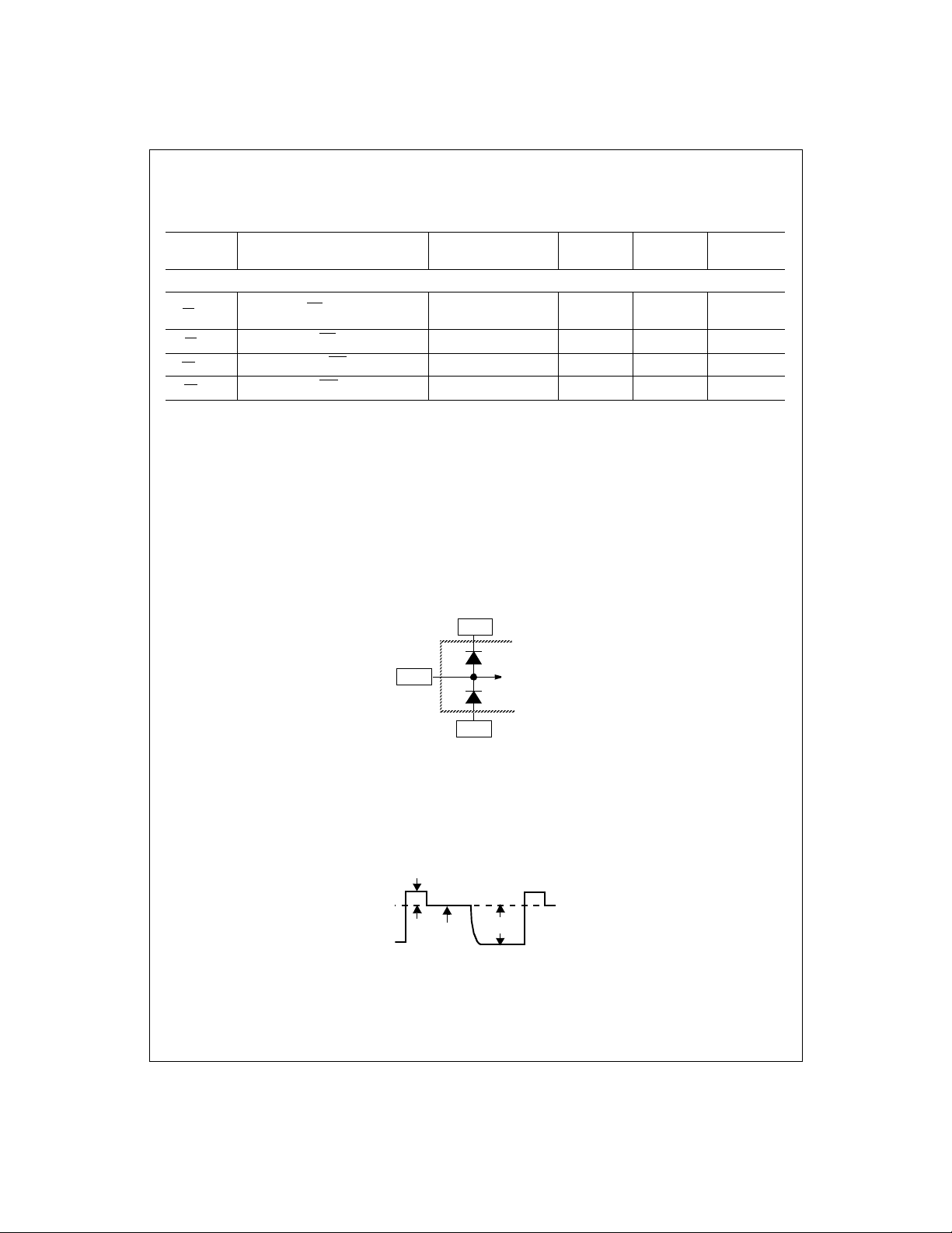
2.0 ANALOG SIGNAL PROCESSING
One channel of the LM9831’s analog front end is shown in Figure
3. The gain through each channel can be set between 0.93V/V
and 9.0V/V us ing r egi sters 3 B, 3C, a nd 3 D. T he offset DAC provides up to ±278mV of offset correction using regi sters 38, 39,
and 3A. The offset DAC and gain stages shoul d be adjusted dur ing coarse calibr ation so that the input signal is a maximum of
1.9Vp-p at the ADC input.
3.0 DIGITAL SIGNAL PROCESSING
3.1 ADC
The digital pixel d ata comes fr om a 6MHz 1 4 bit pipelined A DC.
The output data is formatted as a 16 bit word. The pixel data is in
the upper 14 bits, and the lower two bits are set to 0.
3.2 Pixel Processing Block
The Pixel Proce ssing stage i s used to dig ital ly reduc e the opti cal
resolution of the sensor. The optical resolution can be reduced by
a factor of 1, 1.5, 2, 3, 4, 6, 8, or 12. For a 1200 dpi (optical) system, this would p roduce resol uti ons of 1200 , 800, 600, 4 00, 300,
200, 150, and 100. A 600 dpi (o ptical) system woul d be capable
of 600, 400, 300, 200, 150, 100, 75, and 50 dpi. (Resolution in the
vertical direction is controlled by the stepper motor speed.)
Horizontal resolution reduction is accomplished by averaging
adjacent pixels. Averaging produces better image quality and
reduces aliasing v ersus the traditional technique of s imply discarding pix els to r educe r esolution. For example, t o get 100 dpi
from a 300dpi optical sensor, you would average 3 300dpi pixels:
p
++
pixel
100dpi
n-2pn-1pn
----------------- -------------------------- -=
3
The number of pixels coming out of the Pixel Processing block is
equal to the integer portion of the number of pixels going in to the
Pixel Processing block divided by the “Divide By” setting, from the
table shown in Figure 4.
Pixels
IN
Pixels
OUT
------------------- ------
INT
=
Divide By
This equation also applies to the divide by 1.5 function.
Divide
By
DPI
(1200
DPI
system)
DPI
(800
DPI
system)
DPI
(600
DPI
system)
DPI
(300
DPI
system)
1 1200 800 600 300
1.5 800 533 400 200
2 600 400 300 150
3 400 267 200 100
4 300 200 150 75
6 200 133 100 50
8 150 100 75 37.5
12 100 67 50 25
Figure 4:
Decreasing Horizontal Resolution
If there are not en ough pixel s a t the end of a line to for m a co mplete pixel, the l ast pixel will b e el iminated . F or ex ampl e, if a l ine
is 35 pixels wide and the Horizontal DPI setting is set to divide by
6, then the outpu t of the Pixel Processin g block will be 5 pixe ls
(the integer portio n of 35/6). The last 5 pixels will be discarded,
since 6 pixels would be required to form a new pixel in this mode.
The output of this stage is sent to the Pixel Rate Offset Correction
Block.
3.3 Pixel Rate Offset Correction Block
Offset correction words for every pixel of the CCD are stored in
the external DRAM and acces sed at the pixel rate . A digital s ubtractor subtracts the 16 bit offset word (corresponding to that
pixel’s offset error) from each pixel.
Gain Boost
1V/V or
3V/V
+
+
V
IN
G
Σ
+
V
OS1
B
D
OUT
= (((VIN + V
+
Σ
+
V
OS2
Offset
DAC
simplified, with all offsets = 0, this is:
D
OUT
PGA
0.93V/V to
3V/V
G
Σ
+
V
DAC
+ V
OS1)GB
= (VINGB + V
PGA
+ V
DAC
DAC)GPGA
+
Σ
+
V
OS3
OS2)GPGA
+ V
14 Bit
ADC
OS3
D
OUT
)C
C
C is a constant that combines the gain error through the AFE, reference voltage variance, and analog voltage
to digital code conversion into one constant. Ideally, C = 8192 codes/V (16384codes/1.9V).
Manufacturing tolerances widen the range of C. See Electrical Specifications.
Figure 3: Analog Front End (AFE) Model
21 www.national.com
Page 22

The subtractor saturates at 0, i.e. if the coefficient to be subtracted is gre ater than the ADC ou tput c ode, the r esul t is an output of 0.
The offset words stored in DRAM are typically calculated by
scanning a black calibration strip at 14 bits, and storing the
results in the DRAM using the DataPort.
The offset subtractor onl y uses the upper 14 bits of the 16 bit
word. When scanni ng in 14 bit mode , a pixel is transmitted as a
16 bit word, with the upper 14 bits containing the image data. The
2 LSBs of the image data and the offset correction word shoul d
be 00.
The offset correction equation is:
Pixel
PixelINcoefficient
OUT
–=
3.6 Pixel Packing/Thresholding Block
Some scans require only one bit per pixel (“line art” mode), others
may need only 2 or 4 bits/pixel. To increase scanning speed for
lower pixel depths, the LM9831 packs the desired MSBs of multiple pixels together into 1 16 bit word, increasing the transmission
speed to the host by a factor of 2, 4, 8, or 16. Figure 6 shows how
the pixels are packed together for 8, 4, 2, and 1 bit pixel depths.
In Figure 6, “b” indicates the bit position (b7 = the most significant
and b0 = the l east sign ificant b it) of t he origi nal 8 bi t pixel data,
and p
indicates the original pixel sequence, i.e p0, p1, p2, p3...
n
If there are not enough unpa cked pixels at the end of a line to
complete the pac ked wor d for tr ans miss ion, that fi nal word is no t
sent. For example, doing an 8 bit pixel rate s can with a HDPI
divider of 1 and an o dd number of pixels will tr uncate the blue
component of the last pixel.
3.4 Pixel Rate Gain Correction Block
This is a digital mul ti plier that m ultipl ies the output wor d from th e
subtractor by a 16 bi t digital correc tion coefficient c orrespondin g
to that pixel’s gain error. The coefficients are stored in the external RAM and accessed at the pixel rate.
The multiplier satu rates at 16383, i .e. if the result of the multipl ication is greater than 16383, the multiplier output is 16383.
The gain equation is:
coefficient
Pixel
OUT
Pixel
⋅=
IN
------------------ -------- 16384
Note that a coefficient of 0 represents a gain of 0. On the LM9830
and previous par ts, a co efficient of 0 r epres ente d a gai n o f 1. To
achieve a gain of 1, the coefficient should be set to 16384.
3.5 Gamm a Correction Tables
There are 3 gamma l ookup tabl es for R, G, an d B. The input t o
the table is the 12 MSBs (mos t signi ficant b its) of the 14 bit pi xel
data coming from the prev ious stag e (
rection Block
). The output is the 8 bit gamma correc ted pixel
3.4 Pixel R ate Gain Cor-
data. The tables consume 12k words (4K bytes x 16 bits, only the
8 LSBs of each word is used) of the external DRAM. Each
gamma table (red, gr een , and b lue) c an be loaded with any arbitrary user-defined transfer curve.
255
8 Bit Pixel Out
0
0 4095
The gamma tables ar e lo aded throu gh the da tapor t (see
12MSBs of 14 bit Output
Figure 5:
Gamma Table
6.1 The
DataPort: Reading and Writing to Gamma, Offset, and Gain
). The DataPort selects which color (Red, Green or Blue)
Memory
gamma table will be read from or written to.
Pixel
Depth
bit15bit14bit13bit12bit11bit10bit9bit
8 b7 p
4 b7 p0b6 p0b5 p0b4 p0b7 p1b6 p1b5 p1b4 p
b6 p0b5 p0b4 p0b3 p0b2 p0b1 p0b0 p
0
2 b7 p0b6 p0b7 p1b6 p1b7 p2b6 p2b7 p3b6 p
1 b7 p0b7 p1b7 p2b7 p3b7 p4b7 p5b7 p6b7 p
8
0
1
3
7
bit7bit6bit5bit4bit3bit2bit1bit
0
8 b7 p
4 b7 p2b6 p2b5 p2b4 p2b7 p3b6 p3b5 p3b4 p
2 b7 p4b6 p4b7 p5b6 p5b7 p6b6 p6b7 p7b6 p
1 b7 p8b7 p9b7 p10b7 p11b7 p12b7 p13b7 p14b7 p
Figure 6:
The gamma table in
b6 p1b5 p1b4 p1b3 p1b2 p1b1 p1b0 p
1
Packing Multiple Pixels Into One Word
3.5 Gamma Correction Tables
1
3
7
15
allows the
user to set the threshol d of each tran sition for vario us line art or
reduced pixel depth modes.
3.7 14 Bit Output Mode
For calibration purposes, it is useful to get the 14 bit data from the
ADC. This mode is set thr oug h register 9, bit 5. In th e 14 bit output mode, the gamma and pixel packi ng stages are bypas sed,
and the 14 bit data from the ADC is stored in DRAM, formatted as
shown in Figure 7.
MSB 151413121110 9 8
b13 b12 b11 b10 b9 b8 b7 b6
LSB76543210
b5 b4 b3 b2 b1 b0 0 0
Figure 7:
14 Bit Output Mode Data Format
The 14 bit data is stored as a 16 bit word, with the 2 least significant bits of the 16 bit word set to 0.
3.8 Line Buffer
The line buffer use s the external DRAM as a FIF O line bu ffer to
store the pixel data (whi ch is gener ated at a fixed rate, s ynchronous to the CCD clocks) and send it back to the PC at an asynchronous, unpredictable, and non-constant rate.
The LM9831 s upports 2 sizes of DRA M, 256k x 16bit and 1M x
16bit. 216kbytes (108kwords) of the capacity of the DRAM is consumed by the offset and shading coefficients and the gamma
22 www.national.com
Page 23

tables. That leave s 296kby tes of mem ory av ailabl e for line buffer
4
FSPI
StepSize
pixels/line
X
⋅
------------------ ------------------
=
when using a 256k x 16 bit DRAM, or 1832kbyte s of memory
when using a 1M x 16 bit DRAM.
The line buffer is tig htly coupl ed to the stepper motor (
per Motor Con tro ller
), and is responsible for stopping the motor
4.0 Step-
before the buffer overflow s and starting the motor again as the
buffer nears empty.
If the scanner i s generating pixel data faster t han the PC can
acquire it, the line buffer will start to fill up. As the buffer nears
100% of its capacity, the scan must be paused before it starts
acquiring a line which will overflow the buffer. This Pause Threshold limit (register 4E) is programmable in 2 kbyte (256k x 16 bi t
DRAM) or 8kbyte (1M x 16 bit DRAM) increments between 0 and
255.
To maximize scanner performance and mini mize pausi ng due to
buffer full conditions, the pause threshold should be set using this
formula:
Pause Threshold (kB) = Available_Memory - (Line_Length + 1)
where Available_Memory = 296kbytes (256k x 16b DRAM) or
1832kbytes (1M x 16 bit DRAM),
Line_Length = (Bytes/Line)/102 4
Data Pixels
------------------- ---------------- -
Bytes/Line 2 INT
=
⋅
INT
HDPI_Divider
-------------------- --------------------------------- ------------------ -
CB⋅⋅
16
Where C = 1 for “1 Channel Grayscale”, 3 for all other modes,
Data_Pixels = Data Pixels End (register s 24, 25) - Data Pixels
Start (registers 22, 23)
HDPI_Divider = Horizontal DPI divider = 1, 1.5, 2, 3, 4, 6, 8, or 12
B = Bits per Pixel = 16 (14 bit mode), 8, 4, 2, or 1
Register 4E value = Pause Threshold (kB)/2 (256k x 16 DRAM)
or Pause Threshold (kB)/8 (1M x 16 DRAM)
When the Pause Thr eshold is reached t he buffer sends a c om-
mand to the stepper motor controller to stop scanning. The
remainder of the l ine being processed will c ontinue being processed and be sent to the buffer. If the Lines To Process After
Pause Scan Sig nal register (reg ister 54) is grea ter than 0, then
room for these additio nal lines needs to be adde d into the Pause
Threshold value calculation.
Note that the scanner software on the host PC must set a Pause
Threshold value lo w enough to ens ure that any data that comes
after a pause request (the r es t of the current l ine and any subs equent lines if register 54 bits 0-2 are greater than 0) will fit into the
DRAM buffer. If the Pause Thres hold is set too high, the Lin e
Buffer may overflow, creating discontinuities in the scanned
image.
After a pause, the buffer wi ll continue to tra nsmit data to the P C
until it hits the Resume Threshold limit (register 4F), which is also
programmable in 2 kbyte (256 k x 16 bit DRAM ) or 8kbyte (1M x
16 bit DRAM) increments between 0 and 255. When the Resume
Threshold is reached, the Line Buffer sends the motor controller a
command to resume.
4.0 Stepper Motor Controlle r
The stepper motor controller sends a series of pulses to the stepper motor to move the pa per past the sensor (sheetfe d) or the
sensor past the paper (flatbed). T he speed at which the paper
moves relative to th e sensor, combined wi th the integr ation time
of the image sen sor, determines the effective ve rtical resolution
(Lines Per Inch, or LPI).
The stepper motor is moved forwards and bac kwards by two signals, A and B, 90° out of p hase with each other. The phas e for
the forward direction is set in Configuration Register 45.
The A and B sig nals a re ei ther s quarewav es (in Full S tep Mode ,
Figure 8), or a staircase approximation of a sine wave (in
Microstep mode, Figures 10 and 11).
A
A
1 full step = 4
microsteps
B
B
Figure 8:
Stepper Motor Waveform - Full Stepping
The LM9831 always counts stepper motor steps in units of
microsteps. A full step is equal to four microsteps. Even when the
LM9831 is in Full Step Mode, it is counting in microsteps, and will
increment the s tepper motor (gener ating a full step ) every four
microsteps.
The microstep Step Size is defined in units of time. These units of
time are pixel period s, as defined i n the horizontal pi xel counter.
In the 3 Channel Pixel Rate input mode, the pixel period is the
f
/3 (= f
ADC
modes, the pix el period is equa l to f
Size is stored i n the
/24). In the 3 Channel Line Rate and 1 channel
MCLK
Scanning Step Size
(= f
ADC
/8). The Step
MCLK
configuration register
as a 14 bit v alue. Duri ng normal operation, the stepp er motor is
advanced 1 microstep every Step Size pixel periods. The LPI can
be calculated as follows:
Where FSPI = the number of full steps required to move the
image one inch, pixel s/lin e is the numb er of pixel pe riods it tak es
to scan one horiz ontal line (equivalent to the val ue stored in the
Line End
registers), StepSize is the number of pixel peri-
ods/microstep, and X = 3 for line rate and 1 for pixel rate modes.
Whenever the stepper motor has been moving and then comes to
a stop, the LM983 1 waits for the tim e specifi ed in the H old Current Timeout register and then de -asser ts the A, B, A
, and B outputs to cut power to the motor. When the steppe r motor is not
scanning or fast-feeding (Command = 00), A, B, A
, and B are de-
asserted in all stepper modes.
There are two modes of stepper motor operation: fullstepping and
microstepping.
4.1 Full Step Mode
In Full Step Mo de th e ou tput is a pulse s tream, as s hown i n Fi gure 8. The a mplitude of th e pulses is controll ed by the out put of
23 www.national.com
Page 24

the 2 bit DAC, shown in Figure 9.
noise generated by the driver transistor turning on.
Scan Mode DAC Voltage
0.465V for number of steps specified
Starting from
a dead stop
in Kickstart Steps register (0-7). If
register is 0 there is no Kickstart
current-movement begins at 0.325V.
Scanning 0.325V
0.110V for number of steps specified
Stopped
in Hold Current Timeout register (1 -
31), 0V after time out.
Figure 9:
Full Step Current Control
4.2 Microstep Mode
Microstepping is a tec hnique of dr iving th e steppe r motor with a
staircase approx imation of a sine wave, as s hown in Figure 10.
This technique maximizes the torque of a given motor, resulting in
a higher maximum spe ed. In addition, it in creases the resol ution
of the stepper moto r. If a steppe r motor m oves 3 .6° per ful l step ,
microstepping can create pos itions insi de the 3.6° : 1.8°, 0.9° , or
0.45°, for examp le. This increases the maximu m vertic al resolution of the sc anner. Microstepping also res ults in quieter motor
movement.
A
A
1 microstep
B
DAC
A
A
DAC
B
B
Figure 11:
Stepper Motor Waveform - LM9831 Signals
Figure 12 sho ws the LM 9831’s DAC v oltages. T he peak c urrent
through the ste pper motor winding w ill be 0.465V/R
table index is incremen ted every mi crostep (StepSize pi xel peri-
SENSE
. The
ods).
Table
Index
A (B) A
(B)
DAC
Voltage
000N/A
1 1 0 0.175V
2 1 0 0.325V
3 1 0 0.425V
4 1 0 0.465V
-0 0 0 N/A
-1 0 1 0.175V
-2 0 1 0.325V
-3 0 1 0.425V
-4 0 1 0.465V
Figure 12:
Microstepping Current Control
B
Figure 10:
Bipolar Microstepping Waveform
The amplitude of the microstepped sine wave is controlled by the
output of t he stepper motor D AC (Figur e 11). The current in th e
stepper motor winding is measured as a voltage across the sense
resistor, and the transistor drive signals are pulse widt h modulated (PWM) to force the average current thr ough the winding
equal to V
PWM, and Register 57 controls the minimum time the driver is on
DAC/RSENSE
. Register 56 controls the frequen cy of th e
every period. Re gister 57 shoul d be s et as sh ort as p ossib le, th e
driver only needs to be on lon g enough to mask any transien t
4.3 Pause Behavior - Non-Reversing Mode
When the
Full Steps to Reverse When Buffer is Full
register is
0, the stepper motor sim ply stop s movin g when the P ause si gnal
is received, as shown in Figur e 13. The line of data currently
being processed (section “a” in Figure 13) will continue to be processed and stor ed in DRAM. Additional lines ma y be digitized
and stored as well, depending on the number programmed in the
Lines to Process After Pause Scan Signal
regi ster (Figure 14).
This value is different for different scanner designs and should be
empirically set to the val ue that minimizes the spatial dis tortion
created by the motor slowing down and stopping.
TR
abcd
Microstep
Pulse
Pause
Scanning
Signal
Figure 13:
Stepper Motor Stopping
24 www.national.com
Page 25

Value Ad ditional Lines to Store in DRAM
0 0(a only)
1 1 (a and b)
2 2 (a, b and c)
... ...
77
Figure 14: Lines to Process after Pause Scan Signal
When the Re sume Scan signal is recei ved, the stepper motor
controller waits the appr opriate num ber of pixel periods after the
next TR pulse and then starts step ping again at the normal rate .
The first new lin e trans mitted i s determi ned by the
card After Resume Scan Signal
must be the same as the value in the
Pause Scan Signal
TR
Microstep
Pulse
Value First Line to Transmit After Pause
0b
1c
2d
... ...
7i
Figure 15: Lines to Discard After Resume Scan Signal
4.4 Pause Behavior - Reversing Mode
If the
Full Steps to Reve rse W hen Buffer is F ull
then the Reversing Mode is enabled.
The Reversing Mode eliminates spatial distortion due to the
pausing of a scan. When the Pause Sca n signal is received, the
line curren tly being proc essed is comp leted and stor ed in RAM
(line “b” in Figure 17). When the scan resumes, ideally the
LM9831 would send out lin es “c” and after under the ex act sam e
speed and positional conditions the scanner was in before the
scan paused (as indicated by the dotted line in Figure 17).
When the Pause Scan s igna l is receive d, the LM9 831 pr ocesses
the remainder of the line currentl y being re ad from the CCD (line
b), and stores th e offset (in pixel periods) betwee n the last TR
pulse and the last step . It then stops, revers es, stops, and waits
for the Resume Scan signal. Once Resume Scan is asserted, the
motor controll er waits for the p revious ly stored n umber of p ixels
periods, then s tar ts mo vi ng forwar d ag ain, ma intaini ng the sam e
phase relations hip between the TR puls e and the steppe r motor
control signals. The r esult is as if the stepper mot or had never
paused.
register.
Figure 16:
Scanning
Stepper Motor Resuming
register. The discard value
Lines to Process A fter
abcd
Resume
Signal
Register
Register
Lines to D is-
register is >0,
TR
Microstep
Pulse
Microstep Pulse
(if motor had not
paused)
Stopping, reversing, and resumi ng forward motion all follow the
curve programmed in the
ister. There are 3 segments (Sto pped, 25%, and 5 0%), and the
number in each register indicates the number of full steps to stay
at that acceleration. A value of 0 indicates that that segment is to
be skipped. For example, a value of 0 in all three registers would
mean that the motor would in stantly reverse when the buffer is
full, then instantly stop after going bac k the specified number of
lines.
Speed
Register
Stopped
(x = 0 to 3)
25%
(y = 0 to 3)
50%
(z = 0 to 3)
This acceleration profil e is used any time the motor is started,
stopped, or reversed.
The acceleration profile for stopping, reversing, stopping, and
going forward again is this:
• Full speed forward (1 micros tep = #pixels in
register) until the Pause Scanning signal is received.
Size
• 50% speed forward for z full steps (1 microstep = 2* #pi xels in
Scanning Ste p Size
• 25% speed forwar d for y full ste ps (1 mi crostep = 4*#pixels in
Scanning Ste p Size
• Stopped for x full steps (1 microstep = #pixels in
Step Size
• 25% speed backward for y full steps (1 microstep = 4*#pixels in
Scanning Ste p Size
• 50% speed backward for z full steps (1 microstep = 2* #pixels in
Scanning Ste p Size
• Full speed b ackwar d (1 m ic rostep = #pi xe ls i n
register) for number of microsteps in the
Size
register
Reverse
• 50% speed backward for z full steps (1 microstep = 2* #pixels in
Scanning Ste p Size
• 25% speed backward for y full steps (1 microstep = 4*#pixels in
abcd
Pause
Scanning
Signal
Figure 17:
Figure 18: Acceleration Profile Settings
register).
Reversing - The Goal
Accelerati on Profile
DAC output
x = number of full step clocks to wait
before reversing motor.
y = number of full steps at 25% of final
speed. Full step period = 4 full step
clocks.
z = number of full steps at 50% of final
speed. Full step period = 2 full step
clocks.
register)
register)
register)
register)
register)
configuration reg-
e
Scanning Step
Scanning
Scanning Step
Steps to
25 www.national.com
Page 26

Scanning Ste p Size
register)
• Paused until a Resume Scan signal is received, whichever
event happens first. During the hold curr ent ti meout p eriod, th e
DAC output i s held at 0.110V (the hold c urrent) for FullStep
mode, or the DAC outputs are hel d as they were prior to stopping for the microstep mode. After the hold current timeout
period, output drivers A, B, A
, and B will be deasserted.
• Wait for Resume Scan signal
• Wait for correct number of pixel periods to resynchroni ze stepper motor with sensor timing.
• 25% speed fo rward for y full s teps (1 m icrostep = 4*#pixe ls in
Scanning Ste p Size
register)
• 50% speed forward for z full steps (1 microstep = 2* #pixels in
Scanning Ste p Size
• Full speed forward (1 micros tep = #pixels in
register), w ith T R pulses synchroni zed to same t he pos i-
Size
register).
Scanning Step
tion on image that they would have been had scanner not
stopped.
The
Lines to Process Afte r Pause Scan Signal/Lines to Dis-
card After Resume Scan Signal
register is not used in reversing
mode.
4.5 Fast Feed Step Size Register
When the motor is being moved quickly (
End/Paper Feed to Beginning
Start of S can
register), th e microstep period comes from this
command or
Paper Feed to
Steps to Skip at
register.
For all other motor m ovement, the mic rostep size is gi ven in the
Scanning Step Size
register.
4.6 Stepper Motor Current Control Using PWM
There is an option to use Pulse Width Modulation of the current in
the stepper m otor to increase high s peed torque, optimi ze efficiency, and allow use of a lower current, les s expensive motor.
Precisely controlling the current in the motor provides several
benefits. In Full Step Mode, the motor can start moving faster and
overcome inert ia by increasing th e current to the motor to 100%
when it is sta rting from a dead s top. After a prog ram mable n umber of steps, the inertia is overcome and the current can be
reduced to 70% to reduce heat in the stepper motor (al lowing a
less expensi ve motor to be used). W hen stopping the stepper
motor, the current is increa sed to 100% for a s hort time to o vercome the forward momentum, then the motor is held in position
with a low-level standby current of 25%. If the motor is motionless
for more than the Hold Current Timeout per iod, the current goes
to 0%.
In microsteppi ng mode, th e PWM is used to appr oximate a s ine
wave as shown in Figure 10.
The current control is accomplishe d by measuring the average
motor winding cur rent through a sense resistor to ground, c omparing it to a reference voltage, and PWMing the motor driver
transistor(s) to forc e the c urrent to be equal to the ref erence current. See the
Stepper Motor Current Controller Block Diagram
at the end of this document.
5.0 Scanner Support Function s
5.1 Illumination Control Block
Scanner systems require an illumination source to supply the
light to the image being scanned. This source may be white (typically a fluorescen t lamp), or red, g reen, and/or blue LEDs. Th ere
are four illumination modes in the LM9831:
Illumination
Mode
0
LAMP
This is the power-on default.
Description
, LAMPG, LAMPB outputs = 0.
R
Scanning with white light:
and LAMPB controlled by
LAMP
R
1
LAMP On/Off pointers in horizontal
pixel counter (as in Mode 3),
LAMP
is a PWM pulse stream
G
Scanning with 3 LEDs in color:
LAMP
turns on for Red lines
2
3
Figure 19:
In Illumination Mode 1, the lam p connected t o the LAMP
controlled by the LAMP
ister. The LAMP
the lamp is suppos ed to be on all the ti me, then the On se tting
output (if used) is con trolled the same w ay. If
B
R
turns on for Green lines
LAMP
G
LAMP
turns on for Blue lines
B
Scanning with 3 LEDs in gray:
LAMP
turns on for all lines
R
turns on for all lines
LAMP
G
LAMP
turns on for all lines
B
Illumination Modes
pin is
On/Off settings in the configuration reg-
R
R
should be set to a number between 0 and the value in the Line
End register, and the Off register should be set to a number
greater than the value i n the L ine End r egist er. Converse ly, if the
lamp is supposed to be off all the time, then the On setting should
be set to a number greater than the value in the Line End register,
and the Off register should be set to a number between 0 and the
value in the Line End register. The LAMP
Width-Modulated puls e stream whose dut y cycle is controlled by
output is a Pulse-
G
the value in the PWM register (0 -4095). The dut y cycle is therefore equal to the register value/4096. The PWM counter is
clocked with the 48MHz clock so the output frequency is
48MHz/4096 = 11.7kHz. This PWM output can be used to control
the brightness of a fluorescent lamp.
TR
LAMPR (LAMPR On < Line End, LAMPR Off > Li ne End
LAMP
G
LAMPB (LAMPB On > Line End, LAMPB Off < Line End
Figure 20:
Illumination Mode 1
In Illumination Mode 2 (which is typically used in conjunction with
1 Channel Color
), the LAMP
cycled through sequenti ally, one line at a time. An internal color
, LAMPG, and LAMPB outputs are
R
counter keeps track of the color of the line to be integ rated, and
takes that color’s LAMP output high when the pixel counter
reaches the value stored in th at color’s LAMP On regist er (Configuration Regis ters 2C-37). If the On v alue is greater than the
value in the Line End register, then that lamp never turns on. That
color’s LAMP outpu t goes low when the pixel counter reac hes
that color’s Off va lue. If the Off value is g reater tha n the v alue in
the Line End register, then the pixel counter w ill never reach the
26 www.national.com
Page 27

Off value and the lamp will alway s stay on. Illuminati on Mode 2
timing is shown i n Figu re 21, and in slightly mor e deta il in F igur e
33.
TR
LAMP
R
LAMP
G
LAMP
B
Figure 21:
Illumination Mode 2
Illumination Mode 3 is simi la r to Il lu mination Mod e 2, ex cept tha t
the LAMP outputs fo r all thre e colors are turned on and off every
line. Illuminati on Mode 3 ti ming is shown i n Figures 22 a nd 23.
The Lamp On and Lamp Off settings work the same as in Mode 2
to control the on and off points for the different lamp si gnals. In
systems with a limited power budget, care should be taken to prevent turning multiple lamps on at the same time. This can also be
important for CIS se nsors that limi t the maximum combined current of the three lamps.
TR
LAMP
R
18 for more details on the timing of specifi c sign als. The LM9831
features:
• Independent control over the polarity (inverting or noninverting)
of the input stage to accommodate CIS or CDS signals.
• Full timing control of the CIS and CDS sample points. Refer ence and signal sample points can be inde pendently adjus ted.
Note that the absolute time between re ference sample and signal sample must be 2 MCLKs or grea ter, whether CDS is on or
off.
• Ability to turn off CDS. When CDS is on, traditional CDS is performed. When CDS is off, the signal is sampl ed at the Sample
Signal point, but the i nternal refer ence is used fo r the Sample
Reference voltage (not a point on the input signal itself).
• The CP1 output su pplies the CP pulse nee ded on s ome po pular Toshiba CCDs. This looks and acts just like another, independent RS pulse.
• A CP2 output i s another indepe ndent pixel rate pul se that (if
needed) can be programmed to supply an additional clock.
• CCD clock signals RS, CP1, CP2 are reset when Line Ends
• The internal Clamp signal is reset with Optical Black Pixels
End.
• TR1 and TR2 pulse widths are always the same width, as
determined by Register 0E.
• The TR-Ø1 guardband may be equal to 0, causing TR and Ø1
to go high simultaneously and low simultaneo usly (Figure 24).
This is a requirement of some Canon CIS sensors.
LAMP
G
LAMP
B
Figure 22:
Illumination Mode 3 (grayscale)
TR
LAMPR (LAMPR On > Line End, LAMPR Off < Line End
LAMP
G
(LAMPB On > Line End, LAMPB Off < Line End
LAMP
B
Figure 23:
Illumination Mode 3 (green only)
These modes are in oper ation when ever the chip is powered on
and not in standby mode. For example, the LAMP outputs in Figures 21 and 22 keep pu lsing w hether the LM9831 i s in the Idle,
Paper Feed, or Scann ing states. This el iminates light ampl itude
variations due to the lamp/LEDs war m-up characteris tics. Since
the LAMP pulses are synchronized to the TR pulse, which is
determined by the horizontal pixel coun ter, this means that the
pixel counter is co nstantly runni ng, and any new scans can only
be started by waiting fo r the next new line (the nex t Red line in
the case of Illumination Mode 2).
5.2 CCD/CIS Control Block
This function generates the clock signals necessary to control a
CCD or CIS sensor. Refer to the descriptions for regi sters 0B to
TR
ø1
TR Pulse same as first clock pulse
Figure 24:
TR-Ø1Guardband Can Be Equal To 0
• CIS TR1 Timing Mode 1. In th is mode the T R1 pu lse is exac tly
one Ø clock long, occurring on the ri sing e dge o f Ø 1. The TR1
pulse width and guardband settings are ignored. For Dyna CIS.
TR1
Ø1
RS
Previous
Line
Figure 25:
Transfer
Phase
CIS TR1 Timing Mode 1
Dummy
Pixels
• CIS TR1 Timing Mode 2. In thi s mode the TR pulse is again
equal to 1 Ø period, but now it is centered around Ø1. The TR
pulse width and guardband settings are ignored. For Canon
CIS.
TR1
/4tø1/4
t
ø1
tø1/4
ø1
t
ø1
ø1 inside TR1 pulse
Figure 26:
CIS TR1 Timing Mode 2
• To pr event sensor saturation, the LM983 1 is always clocking
27 www.national.com
Page 28

the CCD/CIS, except when it is in Reset or Standby (Register 7
bit 2 or 3 = 1).
• There is a bit for
Fake Optical Black Pixels
(register 19, bit 2).
This is used with Dyna CIS sensors. In this mode , the RS output pulses once inside the TR1 pulse, then is held high until the
end of the optical black pixel s. The TR1 pu ls e is exte nded u ntil
the trailing edge of the first RS pulse. This mode works for TR1
only, under all TR1 settings (normal and CIS TR1 Timing
modes 1 and 2).
TR1
RS
Trailing edge of
first RS pulse
End of Optical
Black Pixels
Figure 27: Fake Optical Black Pixels
5.3 AFE Operation
The LM9831 supports the fo llowing op eration m odes, controlled
by registers 26 and 27:
• 3 Channel Pixel Rate Mode. In this mode all three channels are
converted with the multiplex er in fr ont of the ADC switchi ng at
the ADC conversion rate, producing inte rleaved RGB data that
is transferred t o RAM. The ADC runs at MCLK/8, each ch annel’s pixel rate is MCLK/24. Each color has its own offset and
gain coefficients. This mode typically uses Illumination Mode 1.
Pixel-Rate
Multiplexing
ADC
C
C
D
Red Channel
Green Channel
Blue Channel
ADC Out LIne 1: RGBRGBRGBRGBRGB...
ADC Out LIne 2: RGBRGBRGBRGBRGB...
ADC Out LIne 3: RGBRGBRGBRGBRGB...
ADC Out LIne 4: RGBRGBRGBRGBRGB...
Figure 28:
3 Channel Pixel Rate Mode
• 3 Channel Line Rate Mode. In this mode all three chan nels ar e
converted with the multiplex er in fr ont of the ADC switchi ng at
the line rate, producing a line of Red da ta, fol lowed by a line of
Green data, followed by a line of Blue dat a, etc. that is transferred to RAM. The selecte d channel and the ADC bo th run at
MCLK/8. Each color has its own offset and gain coefficients.
This mode typically uses Illumination Mode 1.
Line-Rate
Multiplexing
ADC
C
C
D
Red Channel
Green Channel
Blue Channel
ADC Out LIne 1: RRRRRRRRRRRRRRR...
ADC Out LIne 2: GGGGGGGGGGGGGG...
ADC Out LIne 3: BBBBBBBBBBBBBBBBB...
ADC Out LIne 4: RRRRRRRRRRRRRRR...
3 Channel Line Rate Mode
t
INT (GRE EN )
t
INT (BLU E)
Red Green Blue Red Green
3 Channel Line Rate TR Pulse Timing
TR
RED
TR
GREEN
TR
BLUE
Multiplexer
Channel
Figure 30:
Figure 29:
t
INT (RED)
In the 3 Channel Line Rate Mode three TR pulses are generated.
TR
is the TR1 output, TR
RED
is the CP2 output. In this mode TR pulses for a particular
TR
BLUE
color can be “skipped”, increasing the integration time for that
is the TR2 output, and
GREEN
color. In the example shown in Figure 30, the red channel sees 2
times the integration time of the green channel, and the blue
channel sees 3 times the integration time of the green channel.
Each channel can be ind epend ently pr ogramme d to dr op 0, 1, or
2 TR pulses.
12 12
Ø1
TR
RED
TR
GREEN
TR
BLUE
Figure 31:
3 Channel Line Rate Mode with 2 TR
Pulse Posit ions
Each color ’s TR pu lse ca n be p rogra mmed to oc cur in pos ition 1
(inside Ø1 high) or position 2 (inside Ø1 low), as shown in Figure
31.
• 1 Channel Grayscale: Use s the selected channel’s offset and
gain coefficients for all li nes. 1 Channel Grayscale is us ed to
scan a grayscale images. This mode typically uses Illumination
Mode 1 when us ed with a 3 Channel C olor sens or, or Illumi nation Mode 3 when used with a 1 Channel sensor.
28 www.national.com
Page 29

TR
R LED
G LED
B LED
COEF.
DATA
SC
SC SC SC
SC = selected channel (=green in this example)
Figure 32:
1 Channel Grayscale
• 1 Channel Color: This mod e uses a sens or tied to the B lu e OS
input only. Illumination is switched in RGBRGB pattern at the
line rate. Each color has own digital offset and gain coe fficients
as well as stati c Ga in and O ffset data . Note that there i s a on e
line delay between whe n a line is exp ose d to a color and whe n
pixels of that c olo r are cloc ked out of the sensor. For exa mple,
the Green LEDs should be on while y ou are clocking out Red
pixels. This mode uses Illumination Mode 2.
TR
R LED
G LED
B LED
COEF.
DATA
B
R G B
Figure 33:
1 Channel Color
5.4 External DRAM Interface
The LM9831 s upports two external DRAM s izes: 256 k x 16 an d
1M x 16. Th e DRAM is used for line buffering, gain (shading)
coefficient data, offset coefficient data, and gam ma correction.
48kwords (16k pixels * 3 colors) are used fo r gain coefficients,
and another 48kwords (16k pixel s * 3 colors) for the offset coefficients. Gamma correction co nsumes 12kwords (4k x 3 colors).
The remaining RAM (148kwords = 296kB for 25 6k DRAM, or
916kwords = 1,832kB for 1M DRAM) is used for the circular
image data buffer. The 1M size does no t necessarily provide a
performance advant age (except perhaps when the USB bus is
heavily loaded and I/O is very slow) - the opt ion is th ere to provide an alternati ve to the 256k in case of a s upply shortage of
256k DRAMs.
Because the LM9831 does not use any EDO or Fast Page Mod e
features, it can work with either E DO or Fast Page M ode DRAM .
The LM9831 should work with most 50-60ns 256k x 16 or 1Mx16
DRAM. Examples:
Samsung: KM416C1000C/C-L-5, KM416C1200C/C-L-5,
KM416C1004C/C-L-5, KM416C1204C/C-L-5 (5V)
KM416V1000C/C-L-5, KM416V120 0C/C-L-5, KM416V1004C/CL-5, KM416V1204C/C-L-5 (3V)
Alliance: AS4C1M16E5-50 (5V), AS4LC1M16E5-50 (3V)
Micron: MT4LC1M16E5DJ-5, MT4LC1M16E5TG-5 (3V)
There are 2 scan modes: 8 bit and 16 bit. The 8 bit mode is used
for normal scanning to application software to generate 8 bit gray
or 24 bit color images. The 16 bit mode is used for calibration.
3
WP16
4
5
RP RF
6
48MHz
7
8 bit
16 bit
12
RO RS RG WP8 RP RF
RO RS RP
875ns
RO: Offset Coefficient read
RS: Shading (Gain) Coefficient read
RG: Gamma Table read
WP8: 8 bit pixel write (write 2 pixels as 16 bits
every other cycle)
WP16: 16 bit pixel write
RP: read pixel
RF: refresh
Figure 34:
The ADC always converts at 1/8 of the MCLK frequency (f
/8). The datarate to the DRA M is the ADC rate divid ed by
f
MCLK
the HDPI divider setting (f
set correction data and the gai n correction coefficient data are
DRAM Timing per Pixel
= f
DRAM
/HDPI_DIVIDER. The off-
ADC
ADC
provided at the DRAM datarate.
The DRAM timin g is shown in Figure 34. All the read a nd write
operations shown i n Fig ur e 34 m ust be do ne for ev ery pixel written to DRAM. That limits the pixel datarate to the DRAM to
1/875ns = 1.14MH z. The follo wing equati on must be a dhered to
in order to limit the DRAM datarate to 1MHz or slower:
(MCLK div)(HDPI divider)(Int Time Adj) >= 6
Int Time Adj refers to the value in register 19, and will be discussed in a later se ction. If regist er 19 = 0, then the v alue of Int
Time Adj = 1 (for the purpose of this equation).
16kwords
16kwords
16kwords
16kwords
16kwords
16kwords
4kwords
4kwords
4kwords
148
kwords
768
kwords
Red Offset
Green Offset
Blue Offset
Red Shading
Green Shading
Blue Shading
Red Gamma
Green Gamma
Blue Gamma
Pixel Data
(256k and 1M)
Pixel Data (1M)
16kwords
16kwords
16kwords
16kwords
16kwords
16kwords
160
kwords
768
kwords
Red Offset
Green Offset
Blue Offset
Red Shading
Green Shading
Blue Shading
Pixel Data
(256k and 1M)
Pixel Data (1M)
8 bit Datamode 16 bit Datamode
Figure 35:
Memory Map of External DRAM
5.5 PAPER SENSE and MISC I/O
These 8 pins are used for home and paper sensing, LED displays, user start buttons, etc.
Two pins are dedicated inputs: PAPER SENSE 1 and PAPER
SENSE 2. The other six pins, MISC I/O 1-6, can be configured as
inputs or outputs.
=
29 www.national.com
Page 30

The state of each pin , True or False (1 or 0), is reflecte d in the
Status Register.
These are the configurable aspects of these I/O pins:
• Input or Output function. If this bit is set to a 0, the pin is configured as an input. If th is bit is set to a 1 the pin is co nfigure d as
an output.
• The polarity of the inp ut. If th is bi t i s s et t o a 1 (Act ive Hi gh), a
high level on that input pin will produce a True reading (1) in the
Status Register. If this bit i s set to a 0 (Ac tive Lo w), a low le vel
on that input pin wi ll produce a True reading ( 1) in the Status
Register.
• Level or Edge Sensitive. If this bit i s set to 0 (Level Sensitiv e),
the Status Register wi ll reflect the current stat e at that sensor
input pin. If this bit is set to 1 (Edge Sensitive), the Status Register for that i nput will be True (1) if there were any F alse to
True transitions at tha t sensor input pin sinc e the last ti me the
Status Register was read. Reading the status register clears
the state of all the edge sensitive inputs to False (0).
• PAPER SENSE 1 can be programmed to stop the scan (by
clearing the Scanning bit) when its state (as reflected in the Status Register) chang es from F alse to True. This is useful i n flatbeds to prevent the mot or from tr ying to step p ast the limi ts of
travel of the system. In sheetfed systems, PAPER SENSE 1
can be used to detect whether or not the user has inserted a
document to be scanned.
• PAPER SENSE 2 can be programmed to stop the scan (by
clearing the Scann ing bit) and set i ts bit in the Sta tus Register
to True a programmable number of lines after its input pin
changes state from Fal se to True. In shee tfed scanners th is is
useful if the PAPER SENSE is located
before
the scanner array,
where the sensor will chan ge sta tes before all of the paper has
been scanned. For flatbed scanners this sensor can be used to
detect the home position.
• If they are confi gured as outputs, the MISC I/O 1-6 pi ns can
have their output s set to +5V or 0V b y wri ting a 1 or a 0 t o th e
appropriate bit.
The default state of the MISC I/O pins is described in detail in the
Register Listin g section. The M isc I/O p ins revert to their default
states on power-on , after entering USB Suspend, or when th e
RESET pin is pulsed high. A soft reset (register 07) does not
reset the MISC I/O p ins . The de faul t states of t he MISC I/O p ins
are:
• MISC I/O 1: Input, edge sensitive, high-to-low transition sets bit
2 of register 2.
• MISC I/O 2: Input, edge sensitive, high-to-low transition sets bit
3 of register 2.
• MISC I/O 3: Input, edge sensitive, high-to-low transition sets bit
4 of register 2.
• MISC I/O 4: Output, voltage on MISC I/O 4 pin = V
• MISC I/O 5: Output, voltage on MISC I/O 5 pin = V
.
D
.
D
• MISC I/O 6: Output, voltage on MISC I/O 6 pin = 0V.
5.5.1 Adding Function Buttons
Many scanners today feature multiple buttons to select scan,
copy, fax, email, etc. functions. The LM9831’s MISC I/O pin s can
be used for the se func tion s. To free up MISC I/O inputs fo r other
functions, or if more than 6 buttons are required, you can multiplex the buttons together. Figure 36 shows how 7 buttons can be
multiplexed into onl y 3 MISC I/O lines. Figure 37 shows how to
decode the data in register 2 to determine which button was
pressed. This multiplexing technique can easily be scaled to
allow for more or less buttons with the minimum number of MISC
I/O lines.
.
+5V
22k 22k 22k
MISC I/O 1
MISC I/O 2
MISC I/O 3
ABCDEFG
Figure 36: Remote Wakeup With Up To 7 Switches
Switch MISC I/O 1 MISC I/O 2 MISC I/O 3
A0 0 0
B0 0 1
C0 1 0
D1 0 0
E0 1 1
F1 0 1
G1 1 0
Figure 37: T ruth Table for Remote Wakeup Wi th Up To
7 Switches
5.6 The Brains
This is the master cont rol secti on tha t kee ps track of the po sition
of the CCD pixel g oing thr ough the a nalog fr ont end, th e c olor o f
that line of CCDs (for single output CCD illumination control), the
stepper motor, and all other system coordination.
6.0 Communicating with the LM9831
Everything on the LM9831 (configuratio n settings, image data,
coefficient data, and gamma tables) is accessed through the
Configuration Register. Configuration Register I/O is done
through two steps. The first step is to write the address (0 through
7F) of the configuration register to be read from or written to. The
second access is the data operati on (a read or a wr ite) for tha t
address. The a ddress only needs to be w ritten once. After an
address is written , any number of reads and/or writes may be
made to that address.
Registers 0, 1, and 2 are read-only r egisters. Writing to these
addresses may affect vario us counters inside the LM9831 and
should therefore be avoided. Bits 4 of register 3 is also read only,
however it is OK to write to register 3. All of the remaining configuration registers can be read from and written to using this protocol.
6.1 The DataPort: Reading and Writing to Gamma, Offset,
and Gain Memor y
Because the gamma table and the sha ding and offset correction
blocks of RAM are very large, the LM9831 uses an indexed
30 www.national.com
Page 31

method of reading and writing them, called the Data Port. Four
addresses in the Configuration Register are us ed to implement
this feature, as shown in Figure 38.
Configuration
Register
Address
3
4
5
6 DataPort b7 - b0
Figure 38:
The DataPort a llows t he user to s elect a memor y blo ck ( gamma ,
gain coefficient, or offset coefficient) and color (red, green, or
blue) to be read fr om or written to, by writing to Configuration
Register Address 3.
The starting address of th at block ( usually 0) is written into the
DataPort Address register (at Co nfiguration Register Addresses
4 and 5). Bit D6 o f register 4 s hould also be set to a 0 or a 1 to
indicate whether the DataPort will be read from (D6 = 1) or written
to (D6 = 0) in subsequent operations. This is required so the
LM9831 can prefetch the data for faster access. The DataPort
Address is autom atically increme nted after ev ery word ( 2 byte s)
of Offset, Shading, or Gamma data is read/written.
Once the memory block, color, and starting address are written, a
series of reads or writes to the DataP ort will read from or write to
the selected memory block at maximum speed.
Registers 4 and 5 should always be written to after Register 3 has
been changed.
Reading and writing the Data Port should only be done when the
LM9831 is not scanning (Register 07 = 0).
Name Bits
DataPort
Targe t/
Color
DataPort
Address
(MSB)
DataPort
Address
(LSB)
DataPort
b3- b0
b13 - b8
b7 - b0
6.1.2 DataPort Address
This 14 bit register (at Configuration Register addresses 4 and 5)
determines what the starting addr ess is for the read/wri te operation.
This address is automatically incremented after every 2 byte
word read/write oper ation to the actual DataPort.
table the range is 0 to 4093. For the Gain and Offset Coefficients
this range is 0 (corresponding the first valid pixel as programmed
in the Valid Pixels Start register) to 16383 (the maxi mum num ber
of image pixels). If reads or writes continue pas t 4093 or 16383,
the DataPort address counter wraps back around to 0 and continues counting.
6.1.3 DataPort
The DataPort is the 8 bit register (Configuration Register address
06) where the data is sequentially read from or written to. The formats for Offset, Gain, and Gamma data are shown in Figures 41,
42, and 43.
76543210 Type
b13 b12 b11 b10 b9 b8 b7 b6 First Byte
b5 b4 b3 b2 b1 b0 0 0 Second Byte
Figure 41:
76543210 Type
b15 b14 b13 b12 b11 b10 b9 b8 First Byte
b7 b6 b5 b4 b3 b2 b1 b0 Second Byte
Figure 42:
76543210 Type
0000b11b10b9b8 First Byte
b7 b6 b5 b4 b3 b2 b1 b0 Second Byte
Figure 43:
DataPort Offset Format
DataPort Gain Format
DataPort Gamma Format
For the gamma
6.1.1 DataPort Type and Color
These 3 bits determine which memory block (gamma, gain, or offset coefficients, Fig ure 39) and wh ich col or of tha t memo ry blo ck
(red, green, or blue, Figure 40) is to be read from or written to.
76543210 Type
------00 Offset
------01 Gain
------10 Gamma
------11 Undefined
Figure 39:
76543210 Color
----00-- Red
----01-- Green
----10-- Blue
----11-- Undefined
Figure 40:
DataPort Target Pointer
DataPort Color Pointer
7.0 The USB Interface
The LM9831 uses the USB (Universal Serial Bus) interface.
Refer to the LM983 1 softwar e package for details on USB co mmunication.
7.1 The USB Pins
Data is recei ved and transmitted thr ough the D+ and D- pins.
These are 3V di fferential signals. Figure 44 shows the recommended circuitry betwe en the LM9831’s D+ and D- pins and the
scanner’s USB connector.
31 www.national.com
Page 32

∗
Optional - forces LM9831 into
suspend mode if USB cable is
not attached to scanner.
LM9831 D+
(pin 84)
LM9831 D(pin 83)
10pF 10pF
LM9831 V
22Ω
22Ω
REGULATOR
(pin82)
1MΩ
1.5k
D+ USB
Connector
D- USB
Connector
∗
Figure 44: Recommended USB Component Values
8.0 Scanning
8.1 Start Scanning - Initiating an Image Scan
An image scan is initiated by writing a Scan command to Register
07. The LM9831 will move the sensor forward the number of fullsteps specifi ed in r egi sters 4A /4B and begi n sc anni ng. S cannin g
ends when the host writes a new command to the command register (Idle, Paper Feed to Start or Paper Feed to End) or when
PAPER SENSE 1 or PAPER SENSE 2 changes state (if programmed to do so).
The line buffer is reset whe n the Scanni ng bit is SET, not when it
is cleared. The host can continue to read stored data out of the
line buffer after a scan has stopped.
Pixel data is read fr om configuratio n register addr ess 00. Regi sters at other a ddresses can b e read during a scan (to read the
LM9831’s status registers, abort the scan, etc.).
If for some reason you want to pause the scan for some length of
time and resume later, do NOT stop the scan (return to Idle). Simply stop reading pixel data . When the buffer fills up, the LM983 1
will automatically stop scanning and turn off power to the stepper
motor (when the delay goes beyond the time specified in the Hold
Current Timeout register).
The last 2 bytes of every line is a status word ind icating how
much data is in the imag e buffer at the time the status wor d was
written. This infor mation i s in the 8 LSB s of t he statu s word , an d
has the same format as Register 01.
8.2 Reconstructing 8 bit Image Data Received By the PC
When reconstru cting an image from the stream of da ta receive d
from the LM9831, i t is us efu l to know the for ma t of the data. The
LM9831 does not perform deinterleaving on the pixel data, it
comes out exactly as the sensor sends it. Deinterleaving must be
performed on the host PC.
For a single output CCD/CIS that outputs one line of data wit h
colors alternating at the line rate, the output format is:
R
, R2, R3, R4,..., R
1
G
, G2, G3, G4,..., G
1
B
, B2, B3, B4,..., B
1
n-2
n-2
n-2
, R
, G
, B
, Rn (line m)
n-1
, Gn (line m + 1)
n-1
, Bn (line m + 2)
n-1
For a triple output CCD/CIS that outputs 3 lines of data (each x
pixels apart in the vertical direction) with colors alternating at the
pixel rate, the output would be:
R
, G1, B1, R2, G2, B2,..., R
1
, G
, B
n-1
, Rn, Gn, Bn
n-1
n-1
with the Red data repr esenting line m+x, the Green data representing line m, and the Blue data repr esenti ng line m- x. “x” is the
separation between lines, which de pends on the physical distance between the R, G, and B sensors and the rate at which the
sensor is moving over the image.
The length of a line of image data sent to the PC depends on several factors:
• The range of pix els to be s canned (Data Pixels ): Data Pi xels =
(Data Pixels End - Data Pixels Start),
• The horizontal resolution set in the configuration register
(HDPI_Divider)
• The number of bits per pixel (1, 2, 4, or 8, called B), and
• The color mode: pixel rate (C=3) or line rate (C=1).
Data Pixels
------------------- ---------------- -
Bytes/Line 2 INT⋅
=
INT
HDPI_Divider
-------------------- --------------------------------- ------------------ -
CB⋅⋅
16
The scanner software on the hos t must strip the 2 byte status
word from the end of each line before reconstructing the image.
8.2.1 Reconstructing 14 bit Image Data Received By the PC
In the 14 bit Data Mode the Gamma Correction and Pixel Packing
stages are bypassed. Each pixel comes out as 2 bytes instead of
1, doubling the amou nt of me mor y needed t o sto re o ne line. The
data format is shown in Figure 45. This mode is otherwise identical to the 8 bit mode. The number of bytes per line in 14 bit mode
is given in this equation:
Data Pixels
Bytes/Line 2 INT
-------------- --------------------- -
()C⋅⋅=
HDPI_Divider
The 14 bit mode is used to acquire 14 bit data fo r accurate gain
and offset calibration.
76543210 Type
b13 b12 b11 b10 b9 b8 b7 b6 First Byte
b5 b4 b3 b2 b1 b0 0 0 Second Byte
Figure 45:
14 bit Data Format
8.3 High Speed Forward
When register 0 7 is s et to a 1, the LM983 1 mov es the m otor forward at maximu m speed (determin ed by the fast feed stepsize,
registers 48 and 49) until a 0 is written to register 07 or either one
of the PAPER SENSE inputs becomes True (if that sensor has
been properly programmed to interrupt scanner movement).
PAPER SENSE 2 can be used to cau se a delayed stop. If the
FullSteps to Scan after PAPER SENSE 2 trips
register is
greater than 0, motor movement will continue for the programmed number of full steps. This can be used to eject paper in
sheetfed scanners.
The LM9831 also fe atures a Prog rammed High Speed Forward
command. This is identi cal to th e High Speed For ward func tion,
except that it will automaticall y stop moving once the motor has
moved the number of lines specified in registers 4A and 4B.
8.4 High Speed Reverse
When register 07 is set to a 2 , the LM9831 moves the motor
backwards at maximum speed (determined by the fast feed stepsize, registers 48 and 49) until a 0 is wri tten to register 07 or
32 www.national.com
Page 33

either one of the PAPER SENSE input s becomes True (if that
T
sensor has been properly programmed to interrupt scanner
movement). The
FullSteps to Scan after PAPER SENSE 2 trips
register is not us ed i n th e Hig h Speed R ever se mode . T his fun ction is generally used to home the sensor in flatbed sca nning
applications.
The LM9831 also featu res a Programmed Hi gh Speed Revers e
command. This is identi cal to the Hi gh Spee d Reverse function,
except that it will automatical ly stop moving once the motor has
moved the number of lines specified in registers 4A and 4B.
8.5 Short Example of a Scan
• PC configures the LM9831 by writing to the configuration registers.
• PC has the LM9831 scan a ca libration image, then c alculates
the calibration coefficients for the scanner.
• PC transmits the calibration information to the LM9831.
• If a sheetfed, the PC now pol ls the LM9831 s tatus register s to
see if there is any paper inserted. If a flatbed, it moves the scan
head to the home position.
• PC sets the Scanning bit in the Configuration Register.
• PC calculates the size of the image to be scanned in bytes,
then reads bulk data from register 00 of the LM9831 unti l it has
read the entire image . If for som e reas on the sca n need s to b e
aborted, the PC writes a 0 to register 07.
• After all image data is read, PC writes a 0 to register 07 to stop
scan.
• If this is a flatb ed scanner, the PC should now send a High
Speed Reverse command to send the sensor back to the home
position. For a sheetfeeder, it can send a High Speed Forward
command to eject the remainder of the image.
• The scanner is now in the idle state.
9.0 Master Clock Source
The timing for the entire chip comes from the CRYSTAL OUT pin.
Typically this pin is used (with the CRYSTAL IN pin) as a crystal
oscillator. The clock fr equency should be 48MH z. This 48MHz
clock is divided by the MCLK divider (register 08), and the divided
output is MCLK (Master CLocK). The MCLK divider range is from
1.0 to 32.5 in steps of 0.5. A configuration register code of 0
divides the clo ck by 1.0, wh ile a code o f 63 divides the clock by
32.5. AT 48MHz, this provides an MCL K range of 1.48MHz to
48MHz and a corresp onding ADC conversion r ate of 184kHz to
6.00MHz. This divider can be used to closely match the output
data rate to the PC’s input data rate, minimizing scan time.
48MHz Third
Overtone Crystal
Ecliptek
EC-T-48.000M
CRYSTAL IN
5pF 15pF
C1 C2
10Ω
1.2µH
300pF
CRYSTAL OU
24/48
= DGND
Figure 46: 48 MHz Crystal Oscillator Circuit
MCLK is used to clock th e vast maj or ity of the L M9831 ’s circuits .
CRYSTAL OUT is directly used i n the USB I/O section, DRAM
timing, and a few subsections w here the hi ghest possible c lock
speed is required (such as the PWM pul se genera tor for the light
source and the stepper motors).
To use the LM9831’s crystal oscillator feature, tie the CRYSTAL /EXT CLK pin to DGND. Figure 46 shows the recommended
loading circuit and values for a 48MHz oscil lator. These component values assume 10 pF of stray capacitanc e between CRYSTAL IN and ground, and 10pF between CRYSTAL OUT and
ground, for a total CRYSTAL IN and CRYS TAL OUT loading of
15pF and 25pF.
When laying out t he crystal oscillator co mponents, always keep
the traces as short as possible, to minimize stray capacitance
and inductive noise coupling, particularly on the CRYSTAL IN pin.
Operation at 24MHz (2 4/48
= VD) is not reliable and should not
be used.
To drive the LM9831 with an external 48MHz clock , tie CRYS-
TAL /EXT CLK (pin 54) to VD, tie CRYSTAL_IN to DGND, and
drive the TTL or CMOS-leve l clock signal into CRYSTAL_OUT
(pin 52).
10.0 INITIALIZATION
10.1 Power On Reset (POR)
POR is generated by the ramp of the V
+5V. A low to high to low signal on the external RESET pin will
supply pins from 0V to
A
also generate a POR. A POR event:
• Resets the USB transceiver. All enumeration and configuration
data will be reset to its default setting.
• The oscillator will start (or continue) oscillating.
• Forces all configuration registers that have defaults (shown as
black boxes in the configuration register tables) to their default
settings (including the Reset and Standby bits). See the Reset
and Standby mode descriptions for more information.
• MISC I/O 1- 3 will be conf igured as inputs and could generate
remote wakeup signals (after the device is initialized).
• MISC I/O 4-6 are configured as outputs.
10.2 Soft Reset
A Soft Reset is generated by setting bit 5 of regis ter 07. A Soft
Reset:
• Stops mos t of the internal clocks inside the syste m to save
power.
• Does NOT stop 48MHz oscillator.
• Resets internal state machines for correct operation after
register changes.
• Stops DRAM r efresh. This will corrupt all the gamma, offset,
gain values, as well as any image data, stored in the external
DRAM.
• Does NOT prevent configuration register read/writes.
10.3 Standby
The LM9831 enters the S tandby mod e by setti ng bit 4 of register
07. Standby Mode:
• Powers down the analog section to conserve power.
• Tristates the stepper motor outputs (re gardless of the state of
register 45, bit4).
• Does NOT prevent configuration register read/writes.
33 www.national.com
Page 34

10.4 Suspend Mode: Entering
Suspend Mode is enter ed when the USB bus h as had no ac tivity
for 3ms. The Suspend state forces the LM9831 into a low current
idle state. Suspend Mode:
• Stops the oscillator.
• Forces all black-box highlighted configuration registers to their
default settings (includi ng the Reset and Standby bits). See
the Reset and Standby mode descriptions for more
information.
• MISC I/O 1- 3 will be c onfigur ed as inputs an d ca n be used as
remote wakeup signals.
10.5 Suspend Mode: Exiting
When the LM9831 exits Suspend Mode:
• The oscillator is restarted.
• The Reset and Standby bits are still set. The driver software is
responsible for clearing them and setting the configuration
registers again to resume operation. All configuration registers
and DRAM data should be re-written after a Suspend
sequence.
When using the ITA function (ITA > 0), use this version of the
equation:
mclk_divider HDPI_divider ITA 6≥⋅⋅
Use this equation to calculate the stepsize for a scan:
scan_stepsize
where vertical_re solution = the des ired vertical resol ution of the
scan, and FSP I = the number of full s teps req uired to m ove the
sensor one inch.
When using the ITA function (ITA > 0), use this version of the
equation to compensate for the ITA function:
scan_stepsize
12.0 QUESTIONS AND ANSWERS
Q Where is calibration done?
A Calibration is done on the host computer.
line_length vertical_resolution
------------------ --------------------------------- ------------------------------- -=
line_length vert_res
---------------- --------------------------------- -------
FSPI 4⋅
⋅
FSPI 4⋅
⋅
ITA 1+()
------------------ ----- -
⋅=
ITA
11.0 USEFUL EQUATIONS
The integration time (t
where pixel_period is the time it takes to clock one pixel out of the
sensor (C = 3 for Pixel Rate Color, and 1 for all other modes):
and line_length is the length of an entire line, measured in units of
pixels. Note that this includes the transfer portion of the line:
These equations apply for any ITA (Integration Time Adjust, Register 19) setting.
To maximize scanner throughpu t, i t is des irabl e to gene rate dat a
at the same rate as the digital I/O to the host PC. Under some
conditions (slow digital I/O, or very high resolution scans), the
time to generate one line may be greater than the maximum integration time. In thi s case, the integrat ion time may be set to a n
acceptable value using th e previous equations, an d the tim e to
process a line extended using Register 19 (the ITA function).
Using the ITA function, the time to process 1 line can be extended
to match the digital I/O rate required:
The maximum DRAM write pixel rate allowed is 1MHz. If you configure the LM9831 to generate data any faster then 1Mpixel/s, the
LM9831 will not fun ction correctly. To ensure that the LM9831 is
programmed to a leg al datarate, ensure that this constraint is
met:
) for 1 line is always:
INT
t
pixel_period line_length⋅=
INT
pixel_period
line_length line_end TR_time
t
LINE
mclk_divider HDPI_divider 6
mclk_div C 8⋅⋅
-------------- ------------------------- -=
48MHz
1+ ITA()t
=
+=
INT
≥⋅
Q Does the LM9831 support 800dpi sensors? 400dpi? XXXdpi?
A Yes. The LM9831 wil l suppor t any se nsor up to a maximum of
16383 pixels x 3 colors. Available horizontal re solutions are
calculated by th e optical resolution of the scanner divide d by
the HDPI_divider.
13.0 GENERAL NOTES AND TROUBLESHOOTING TIPS
(mclk_divider)(H DPI_divid er)(ITA) must be grea ter than or equal
to 6. If this condition is not met, the LM9831 will not work.
Make sure the gamma tables are programmed with a valid
gamma curve.
Make sure the multiplier gain coefficients are loaded and correct.
(Remember, a gain coefficient of 0 means a GAIN of x0, not x1. If
the gain coefficient = 0 the output code will always be 0.)
Remember that w hen the LM9831 is reset (reg08 = 0x 20) or in
suspend for long er than a few mill iseconds (cons ult your DRAM
datasheet), DRA M refres h will stop an d the Gamm a and Co efficient data may be corrupted.
Some of the CCD s ign als (R S, CP1, and CP2) can hav e a sm all
pulse when line_en d occurs. Line_end resets thes e signals and
depending on how they are programmed to go on and off,
line_end can chop off the si gnal before it s programmed off time .
This is not a problem because the truncation occurs at the end of
every line, after all the image data for that line has been digitized.
Registers 4 a nd 5 only autowrap to 0 from the ir h ighe st pos sible
legal address. If an address higher than the highest legal address
is written, it will continue to increment from the illegal address, not
wrap to 0, and unknown oper ation may occur. This can not happen unless the host writes an illegal address to the dataport.
The absolute distance between reference sample and signal
sample must be 2 MCLKs or greater, whether CDS is on or off.
34 www.national.com
Page 35

The range of values for the Optical Black (regi sters 0F and 10),
Reset Pulse (11 and 12) , CP1 pu lse ( 13 an d 1 4), CP 2 p uls e (15
and 16), Reference Sample (17), and Signal Sample (18) settings
depend on the rate of the pixel data coming from the sensor.
Mode Pixel Rate
Pixel Rate Modes MCLK/24 0 - 23
Line Rate Modes MCLK/8 0 - 7
Always make sure li ne length ( data p ixels end - data pi xels start)
is >= the horizontal divider. For example, if you are dividing by 12,
the line length must be >=12.
The Line End (r egiste rs 20 a nd 21) setti ng mus t be progr amme d
as follows rel ative to the Dat a Pixels End ( registers 24 and 25)
setting:
Line End must be >= Data Pixels End + 20
The Data Pixels Start (registers 22 and 23) setting must be >=the
Active Pixels Start (registers 1E and 1F) setting.
The correct Default Phase Differenc e (registe rs 52 an d 53 ) mus t
be set for a scan to restart properly following a pause in the scanning. See th e LM9831 software for informat ion on setting the
DPD register.
The number of fullsteps skipped at the start of a scan may be one
less than the Fu llstep s to Sk ip at S tar t of Scan ( register s 4A an d
4B) setting.
The Scanning Step Size (registers 46 and 47) and Fast Feed
Step Size (registers 48 and 49) settings must be > 2.
When reverse is enabl ed, the LM9831 always stops on Red (lin e
rate color). When reverse is disabled, it will stop on any color.
The contents of register 01 is not reset by the start of a new scan,
but it is update d to the correc t value after the first line has been
scanned. To reset this counter prior to starting a scan, the chip
can be briefly reset (regist er 7 = 0x20). Since resetting the chip
may have undesir ed consequences (turni ng the lamp off briefly,
interrupting DRA M refresh), it is also acceptable to simply wai t
until register 01 s tarts incrementi ng. At that point the registe r 01
data will be correct.
Gamma and gain/offset coefficient data should be written with
reg07=0 (idle). Do not attempt to write gamma or gain/offset coefficient data when scanning (reg07=03).
14.0 PORTING SOFTWARE FOR LM9830 TO LM9831
The LM9831 is similar in architecture to the LM9830. Porting a
TWAIN driver from the LM9830 to the LM9831 is relatively
straightforwar d if consideration is given to the follow ing issues.
The LM9831 includes almost all the features of the LM9830, plus
several new ones. The first step is to change the LM9830 Twain
driver so that it works with the LM9831. The second step is t o
take advantage of t he new fe atur es of the LM9831 that will a llow
you to obtain even better, faster scans than you obtained with the
LM9830.
14.1 Porting Step 1
14.1.1 Adjust for Register Changes
While more than 50% of the regi sters in the LM98 31 are in th e
Registers 0F to 18
Range
same location and perform the s ame function as they did in the
LM9830, many other registers have changed. Sometimes the
address of a register changed, sometimes the location of the bits
inside a register were moved, some regi ster settings were combined or deleted, an d the size of some registers was changed .
Please compare the register listings for the LM9830 and LM9831
carefully. This is a list of registers that have changed:
Registers 1, 2, 3, 4, 7, 9, B, 19, 1A, 1B, 3E-41, 42, 43-44, 4E-4F,
51-53, 54, 5A, 5B, 5E.
14.1.2 Choosing the MCLK Divider (Register 0x08)
The datarate coming out of the Horizontal DPI Divider must be
1.1MHz or less . If it i s faster tha n th is, the LM 9831 wil l not operate correctly. Since the maximum US B datarate is about 1MHz ,
this does not impact the performance of the scanner in any way.
This is the Clock Divider Rule:
(MCLK_divider)(HDPI_divider)(ITA) >= 6.
The ITA (Integration Time Adjust) refers to register 19, and will be
discussed in a later section. If register 1 9 = 0, th en the v alue o f
ITA = 1 for the purposes of this formula.
If register 19 = 0, this formula means that if the HDPI_divider = 1,
the MCLK_divide r must be set to div ide-by-6 (re g 08 = 10 [decimal]) or high er. If the HDP I_divider = 4, the MC LK_div ider mus t
be set to divide-by-2 (reg 08 = 2) or higher. If the HDPI_divider is
6 or larger, then the MCLK_divider can be set to divide-by-1
(reg08 = 0).
See
14.2.2 Integration Time Adjustment Function
tional information.
14.1.3 Calibration
In the LM9830, calibrati on was always performed at the optical
resolution of the scanner. For example, if the optical resol ution of
the scanner was 600dpi, then calibration was performed at
600dpi even if the scan was going to be at 300dpi or 150dpi.
To k eep the s peed of the LM98 31 high while us ing slowe r DRAM
(instead of SRAM) , th e arc hitectur e o f the LM983 1 was ch anged
so that the Horizontal DPI adjust function is performed
pixel rate offset and shading correction, instead of after (as in the
LM9830).
This means that the calibr ation ro utine needs to b e chan ged so
that register 9 is set to the desired scan resolution before calibration.
14.1.4 Pixel Rate Offset Correction
The LM9831 now uses 14 bits for the offset correction of each
pixel. The offset correct ion data is shifted up to fit into the 16 bit
DRAM. For exampl e, offset correcti on codes of 3, 3 1 and 4096
would be transmitted to the dataport as:
0003: 0000 0000 0000 1100
0031: 0000 0000 0111 1100
4096: 0100 0000 0000 0000
for addi-
before
the
35 www.national.com
Page 36

14.1.5 Pixel Rate Shading Multiplier
The shading multiplier uses all 16 bits of data.
There is an importan t difference between the pi xel rate shading
multiplier of the LM 9830 and the LM 9831. In the LM 9830, i f the
value for the shading multiplier was 0, the gain through the multiplier was 1V/V. The LM9830 also had 3 multiplier gain ranges: 1
to 1.5, 1 to 2.0, and 1 to 3.0 V/V.
The LM9831 ha s a simpl er mul tip lier with only one g ain range: 0
to 4 V/V. The gain of the multiplier is
Gain = (gain code)/16384 V/V
Note that if the gain co de = 0, the n the pi xel is multipl ied by 0! In
other words, if the gain coefficient is set to 0, the outpu t of the
multiplier will be all 0s. A gain code of 0 was not unu sual for the
LM9830, but will not work with the LM9 831. To maintain a minimum gain of 1V/V, make sure the gain code is 16384 or higher.
If desired, gains between 0 and 1 V/V can be used, but they will
usually result in less dynamic range and noisier images.
14.1.6 The Gamma Table
The LM9831’s 3 gamma tables are 12 bits wide, instead of 10 bits
(LM9830). Thi s means eac h g amma curv e ha s 4 tim es the n umber of datapoints and you can now get 4 times the accuracy available with the LM9830.
Since most consumer CCDs have a true SNR of less than 12 bits,
the LM9831 does not support a 14 bit gamma table, freeing up an
additional 36kwords of DRAM memory.
14.1.7 General DataPort Information
There have been several important changes to the dataport.
The read-only Pause bit is now in register 3. You can write this bit
in order to w rite to the o ther bits in the regis ter, but anyth ing you
write to the Pause bit will be ignored.
There are now 2 bits to select between O ffset Coefficients, Gain
Coefficients, and Gamma data.
In the LM9830, Offset and Gain coefficients were combined to
make one 16 bit word, written to register 6 as 2 bytes.
In the LM9831, Offset is a 16 bit word, and Gain is a 16 bit word.
Offset and Gain data each have a separate dataport address.
Register 5 will auto increment after 2 bytes are written to register
6 in Offset mode or Gain mode (reg03b1 = 0).
Gamma data is 8 bits wide, as in the LM9830. Register 5 will auto
increment after 1 gamma byte is written to r egister 6 i n Gamm a
mode (reg03b1 = 1).
The bit locations for selecting color (R, G, or B), have been
shifted left by 1 bit.
The DataPort address width is now 14 bits wide. This caused the
R/W bit to be shifted left by 1 bit.
When using 1 Channe l Gr aysca le, the LM 9830 ignored the color
bits in register 3. Thi s has been fi xed in the LM98 31. Regist er 3
controls the gamma table color.
Make sure your software takes all of these changes into account.
14.2 Porting Step 2
Once your TWAIN d river is operatin g with t he LM9831 , you can
start taking advantage of the LM9831’s additional features.
14.2.1 1200 DPI
The LM9831 can support line wi dths up to 16384 pixe ls x 3 colors. This allows 1200dpi scanners with a maximum width of 13.6”
(B-size).
14.2.2 Integration Time Adjustment Function
Due to DRAM speed limitations, the maximum speed at which the
LM9831 can store pixels is 1MHz. The ADC can run at speeds up
to 6MHz, but only when th e HDPI divider is set to divide-by-6 or
greater, which results in a pixel rate of 1MHz or less.
This can be a challenge when scanning at high resolutions. For
example, a 600d pi 8 .5” wide color CCD s c anner di gitiz es 15,300
pixels/line. At a 1MHz rate, the resulting integration time
is15.3ms. Integrati on times above 10ms may be problematic in
some designs.
To allow shorter integration times without violating the 1MHz max
pixel rate, the LM9831 has an Integration Time Adjust (ITA) function (Figure 47). I TA gener ates 2 alternating timebase s for the
CCD timing, a high frequency timebase, and a lower frequency
timebase. During the high frequency timebase, the integration
time (t
divided by 6MHz. (Using the previous example, that would be
2.5ms). During t
digitized by the AFE. The CCD output signal (representing line “n-
) is short, as short as the total number of pixels in a line
INT1
, data is clocked out of the CCD but it is not
INT1
1”) is discarded.
After the short integration time, the clock is s lowed for the next
integration time (t
this period. Since t
pixel data for line “n”. As long as t
of 1MHz or slower, the line can be digitized and written to the
). Integration for line “n+1” is done during
INT2
is longer, there is more time t o read out
INT2
corresponds to a pixel rate
INT2
DRAM.
t
INT1
TR
Pixel
Data
Figure 47:
is determined by th e traditional calculation s, primarily the
t
INT 1
MCLK divider and line end settings. t
line n line n+1line n-1
discard
t
= ITA * t
INT2
Integration Time Adjust Function
INT2
INT1
= ITA * t
t
INT2
line nline n-2
.
INT1
There are two m or e cons iderati ons when using the ITA. The firs t
is CCD image lag. Image lag is a sensor phenomenon in which a
percentage of t he pi xel v oltage f rom the previ ous li ne appears in
the pixel voltage for the current line. In the example above, some
of the signal from line n- 1 will lea k into line n . Since the integr a-
36 www.national.com
Page 37

tion time for line n-1 ( t
leakage may be as much as 2 to 6 times the sensor sp ecified
image lag. This is usually not a problem. If it is, use a sensor with
a low image lag specification, or reduce the brightness of the
CCFL light source.
The second consideration is the stepsize calculation. Using the
ITA’s dual ti mebases affects the s tepsize required to produce an
image with the correct vertical resolution. The solution is to calculate the steps ize using the traditional formula, t hen multiply it by
the factor (ITA+1)/ITA:
stepsize_ITA stepsize
15.0 KNOWN ISSUES AND SOLUTIONS
15.1 14-Bit Data Mode
The 14 Bit Data Mode (register 09, bit 5) has two uses. The first is
for calibration, where very accu rate pixe l data mus t be ac quired
to allow calculation of the offset and shading coefficients. The
second is for scanning images where the pixel data transmitted to
the PC is greater than 8 bits/channel.
The current silicon has two problems in 14 bit mode:
1) When attem pting to read more image d ata than the DRAM
buffer has avail able (unde rflowing th e DRAM) , the LM 9831 may
insert an extr a, random byte of data . This is not predic table or
detectable. The fix is simple: poll register 01 before reading register 00, and only read the amount of data register 01 says is available.
) is 2 to 6 ti mes longer than t
INT2
ITA+1
------------
=
⋅
ITA
INT1
, the
I/O 1, MISC I/O 2, or MIS C I/O 3 inputs was supposed to gener ate a USB Remote Wakeup. While the LM9831 passes the Chapter 9 test for Remote Wakeup, we have not been able to get this
function to work with a PC that is in Suspend Mode. At the time of
release we are still trying to verify functionality of this feature.
For 1M x 16 DRAMs, read (<reg 01> - 1) * 8kbytes of data.
For 256k x 16 DRAMs, read (<reg 01> - 1) * 2kbytes of data.
Note: The i nformation in register 01 (number of bytes of image
data in DRA M b uffer) is not valid unti l the first li ne of i mag e dat a
has been digitized. The solution is to poll regi ster 01 until it starts
incrementing. When register 01 has incremented, the data it contains is valid.
2) When the DRAM buffer ’s address counter “wraps around”, it
may or may not insert 2 extra byte s of bad data . There is no way
to predict when or if this will happen. This limits the size of a continuous scan to the si ze of the DR AM line buffer (148k pi xels or
916k pixels). This means that it is impossible to scan large
images with mo re than 8 bits/channel being transm itted to the
PC. Calibration can be done at 14 bits (since calibration is only a
few lines of data), but you can not reliably transm it 10, 12, or 14
bit images to the PC.
15.2 USB Interrupts
When configured to do so, changes on the Paper Sense and
MISC I/O pins were suppo sed to generate USB Interrupts. This
functionality is not working at the time of this datasheet’s publication. The solution (as demonstrated in our Twain Driver software)
is to poll register 02 every 200 to 500ms. This uses v ery little
additional bandwidth compared to the USB interrupt solution.
15.3 USB Remote Wakeup
When configured to do s o, a high-to-low tran sition on the MISC
37 www.national.com
Page 38

LM9831 Digital Block Diagram
CRYSTAL/ EXT
CLOCK
Pixel
Processing
(Horizontal
DPI adjust)
CCD
or
CIS
Image
Sensor
Analog
Front
End
14
The Brains
RESET
System Synchronization and Control
Pixel Counter, Stepper Counter,
Lamp Counter, Command Interpreter
CRYSTAL
24/48
16
Sensor (Offset and Shading)
Buffer In Address Counter
Buffer Out Address Counter
Line Buffer Controller
OUT
16
Pixel-Rate
Offset
Subtraction
Address Counter
System Clock
Generation
16
48MHz
Pixel-Rate
CRYSTAL
IN
16
16 x 16
Multiplier
(Shading)
Test
Test
Modes
14 Bit
Pixel Data
Gamma
Table
Address
12
17
20
20
Pause Scanning
Resume Scanning
EXTERNAL
EEPROM
SCL
External EEPROM
Internal ROM
Configuration
Registers
DRAM
Address
Multiplexer
and
Controller
SDA
16 16
8
Pixel
Processing
(Packing)
Controller
CMODE
Interface
Stepper
Motor
USB
16
2
10
4
3
3
2
6
D+, DActive/Suspend
Bus Power
D0-D15
DRAM
16
Data Bus
RD
WR
RAS
CAS
A0-A9
DRAM
Address Bus
Power
Transistors
Current
Feedback
Lamp
Control
PAPER
SENSORS 1,2
MISC I/O 1-6
38 www.national.com
Page 39

Analog Front End Block Diagram
RED OS
from sensor
GREEN OS
from sensor
BLUE OS
from sensor
V
REF LO
V
REF MID
V
REF HI
V
BANDGAP
V
REGULATOR
R
G
B
Coarse Color
Balance PGAs
x0.93
to x3
x0.93
to x3
x0.93
to x3
14 Bit
ADC
Sensor
Clock
Generation
14
ø1
ø2
RS
CP1
CP2
TR1
TR2
Gain
Boost
OS
R
1
CDS
x1or x3
-1
OS
G
1
CDS
x1or x3
-1
OS
B
1
CDS
x1or x3
-1
Static
Offset
DACs
+
+
Offset
DAC
+
²
+
Offset
DAC
+
²
+
Offset
DAC
1.5V (CDS)
3.5V (CCD)
Bandgap
Reference
3V (USB I/O)
Regulator
39 www.national.com
Page 40

Stepper Motor Current Controller Block Diagram
Phase A
A
A
DAC code for
phase A
Invert
3
DAC A:
0.110V,
0.175V,
0.325V,
0.425V,
0.465V
Set-Dominant
–
+
S/R Flipflop
Reset
Q
A
+Vmotor
8
CR
6
CR
DAC code for
phase B
B
B
12MHz
÷1 to 256
÷64
PWM
Generator
0/64 to
63/64
high time
3
Phase B
Invert
DAC B:
0.110V,
0.175V,
0.325V,
0.425V,
0.465V
TriState Stepper
Motor Outputs
Set
Comparators need no hysteresis. SR flipflops are set periodically by pulse from PWM Generator. Flipflops can only be reset
after SR goes low when Reset (comparator output) is high
(V
> V
SENSE
Reset is level sensitive, not edge sensitive.
+
–
DAC
).
Reset
Set-Dominant
S/R Flipflop
Set
Q
40 www.national.com
HIGH CURRENT
GND SENSE
LM9831
A
SENSE1
SENSE2
B
B
1Ω
1Ω
+Vmotor
Stepper
Phase A
Stepper
Phase B
Stepper
Phase A
Stepper
Phase B
External Components
Page 41

Physical Dimensions (millimeters)
100-Pin Thin Plastic Quad FlatPac (JEDEC) (TQFP)
NS Package Number VJD100A
Order Number LM9831VJD
LM9831 42-Bit Color 1200dpi USB Image Scanner
LIFE SUPPORT POLICY
NATIONAL'S PRODUCTS ARE NOT AUTHORIZED FOR USE AS CRITICAL COMPONENTS IN LIFE SUPPORT
DEVICES OR SYST EM S W ITHOU T T HE EXPRES S W RIT TEN APPROVAL OF THE P RESIDE NT O F NATIONAL
SEMICONDUCTOR CORPORATION. As used herein:
1. Life support devices or systems are devices or systems which,
(a) are intended for surgical implan t into the body, or (b) support
or sustain li fe, and wh ose fa ilure to p erform wh en proper ly use d
in accordance with instructions for use provided in the l abeling,
can be reasonably expected to result in a significant injury to the
user.
National Semiconductor
N
Corporation
Americas
Tel: 1-800-272-9959
Fax: 1-800-737-7018
Email: support @ nsc.com
http://www.national.com
National Semiconductor Europe
Fax: +49 (0) 1 80-530 85 86
Email: europe. suppor t @ nsc.com
Deutsch Tel: + 49 (0) 1 80-530 85 85
English Tel: + 49 (0) 1 80-532 78 32
Francais Tel: + 49 (0) 1 80-532 93 58
Italiano Tel: + 49 (0) 1 8 0- 534 16 80
2. A critical component is any componen t of a life suppor t device
or system whose fai lure to perfor m can be reasonabl y expected
to cause the failure of th e life support devic e or system, or to
affect its safety or effectiveness.
Nation al Sem i conductor As ia
Pacif i c Cust omer Response
Group
Tel: 65-2544466
Fax: 65-2504466
Email: sea.support @ nsc.com
National Semiconductor
Ltd. Japan Ltd.
Tel: 81-3-5639-7560
Fax: 81-3-5639-7507
National does not assum e any responsibility for use of any circ uitry des cribed, no circuit patent lice nses are implied and National res er ves the righ t at any time w ith out not ice to ch ange sai d circu itr y and sp ecifications.
41 www.national.com
 Loading...