

Page 1
N
LM9830 36-Bit Color Document Scanner
General Description
The LM9830 is a complete docu ment s canner syst em on a single IC. The LM9830 provides all the functions (CCD control, illumination control, analog front end, pixel processing function
image data buffer/SRAM controller, microstepping motor controller, and EPP parallel por t interface) necessar y to create a high
performance color scanne r. The LM9830 scans images i n 36 bit
color, and has output data formats for 36 bits, 30 bits, and 24
bits.
The only additional a ctive components requ ired are an exter nal
SRAM for data buffering and power transist ors for the stepper
motor. Parallel port pass-through requires two additional
TTL/CMOS logic ICs.
Applications
•
Color Flatbed Document Scanners
•
Color Sheetfed Document Scanners
Features
• Scans at up to 6Mpixels/s (2M RGB pixels/sec).
• Digital Pixel Processing provides 300, 200, 150, 10 0, 75, and
50 dpi horizontal resolution from 300dpi sensor, and 600, 400,
300, 200, 150, 100, 75, an d 50 dpi hor izontal resol ution from
a 600dpi sensor.
• Provides 50-600dpi vertical resolution in 1 dpi increments.
• Pixel rate error correction for gain (shading) and offset errors.
• Output formats inclu de 12 bit linear, 10 bit linear with shad ing
and offset, or 8 bit gamma corrected, all with 12 bit accuracy.
• Multiple CCD clocking rates allows matching of CCD clock to
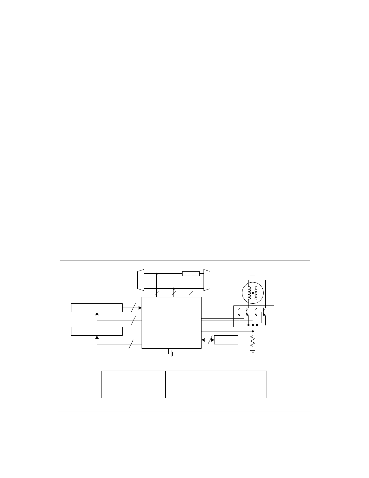
Scanner Block Diagram
To
Computer
CCD/CIS
2-6
Illumination
1-3
DB25
9 28
1-3
LM9830VJD
scan resolution and pixel depth for maximum scan speed.
• Stepper motor control tightly coupled with buffer management
to maximize data transfer efficiency.
• PWM stepper motor curr ent control allows microsteppi ng for
the price of fullstepping.
• Supports 64k, 128k, or 25 6k x8 external SRAMs.
• Parallel Port interface suppor ts EPP, PS2 (bidirection al), or
SPP (nibble) modes of operation.
• Pixel depths of 1, 2, or 4 bits are packed into bytes for faster
scans of line art and low pixel depth images.
• Supports 1 and 3 channel CIS and CCD devices.
• 3 (R, G, and B) user-programmable gamma correction tables.
• Able to transmit an arbitrary range of pixels to speed up
scanning of smaller items (business cards, etc. ) by zooming
in on a subset of CCD pixels.
• Compatible with a wide range of color linear CCDs and
Contact Image Sensors (CIS)
• Internal bandgap voltage reference.
• 100 pin TQFP package
Key Specifications
•
Analog to Digital Converter Resolution 12 Bits
•
Maximum Pixel Conversion Rate 6MHz
•
A4 Color 150dpi scan (typical, EPP Interface) <10 seconds
•
A4 Color 300dpi scan (typical, EPP Interface) <40 seconds
•
A4 Color 600dpi scan (typical, EPP Interface) <160 seconds
•
Supply Voltage +5V±10%
•
Power Dissipation (typical) 350mW
Buffer
DB25
Printer
28
To
SRAM
+24V
November 1998
Stepper
Motor
Power
Transistors
LM9830 36-Bit Color Document Scanner
Ordering Information
Commercial (0°C ≤ TA ≤ +70°C) Package
LM9830VJD VJD100A 100 Pin Thin Quad Flatpac
LM9830VJDX VJD100A 100 Pin Thin Quad Flatpac, Tape & Reel
TRI-STATE® is a registered trademark of National Semiconductor Corporation.
©1998 National Semiconductor Corporation
1
http://www.national.com
Page 2
(
)
Absolute Maximum Ratings
Positive Supply V oltage (V+=VA=VD=V
With Respect to
GND=AGND=DGND=DGND
V oltage On Any Input or Output Pin -0.3V to V
=DGND
I/O
DI/O=VSRAM
SRAM
(Notes 1 & 2)
)
+
+0.3V
Input Current at any pin (Note 3) ±25mA
Package Input Current (Note 3) ±50mA
Package Dissipation at T
ESD Susceptibility (Note 5)
= 25°C (Note 4)
A
Human Body Model 1000V
Operating Ratings
Operating Temperature Range T
LM9830VJD 0°C≤T
6.5V
V
Supply Voltage +4.5V to +5.5V
A
V
Supply Voltage +4.5V to +5.5V
D
V
Supply Voltage +4.5V to +5.5V
DI/O
|V
|, |VA-V
A-VD
|V
D-VSRAM
Input Voltage Range -0.05V to V
DI/O
|, |V
DI/O-VSRAM
|, |VA-V
Soldering Information
Infrared, 10 seconds (Note 6) 235°C
Storage T emperature -65°C to +150°
Electrical Characteristics
The following specifications apply for AGND=DGND=DGND
f
CRYSTAL IN
= 50MHz. Boldface limits apply for T
A=TJ=TMIN
Symbol Parameter Conditions
CCD/CIS Source Requirements for Full Specified Accuracy and Dynamic Range
Sensor’s Maximum Output Signal
V
OS
Amplitude before LM9830 Analog Front
PEAK
End Saturation
Full Channel Characteristics
Resolution with No Missing Codes 12 bits (min)
INL Integral Non-Linearity Error
(Note 11)
DNL Differential Non-Linearity
Analog Channel Gain Constant
C
(ADC Codes/V)
V
V
V
V
Pre-Boost Analog Channel Offset Error,
OS1
CCD Mode
Pre-Boost Analog Channel Offset Error,
OS1
CIS Mode
Pre-PGA Analog Channel Offset Error -30
OS2
Post-PGA Analog Channel Offset Error -21
OS3
Coarse Color Balance PGA Characteristics (Configuration Registers 3B, 3C, and 3D)
Monotonicity 5 bits (min)
(Minimum PGA Gain) PGA Setting = 0 0.93
G
0
(Maximum PGA Gain) PGA Setting = 31 3.05
G
31
x3 Boost Gain
Gain Error at any gain
(Note 13)
I/O
to T
=DGND
MAX
=0V, VA=VD=V
SRAM
; all other limits TA=TJ=25°C. (Notes 7, 8, & 12)
Gain = 0.933
Gain = 3.0
Gain = 9.0
Includes voltage reference
variation, gain setting = 1
x3 Boost Setting On
(bit B5 of Gain Register is set)
Note 12
(Notes 1 & 2)
|, |VD-V
SRAM
|,
DI/O=VSRAM
Typical
(Note 9)
|,
DI/O
=+5.0VDC,
Limits
(Note 10)
2.1
0.65
0.21
-1.1
+4.6
-0.5
+0.7
2048
4
12
-7
+10
-0.9
+2.0
1863
2129
-21
+34
-15
+38
-58
+8
-59
+14
.90
.96
2.98
3.15
2.99
2.86
3.08
±0.2 ±1.6 % (max)
≤
T
MIN
A
≤
100mV
+
+ 0.05V
LSB (min)
LSB (max)
LSB (min)
LSB (max)
LSB (min)
LSB (max)
mV (min)
mV (max)
mV (min)
mV (max)
mV (min)
mV (max)
mV (min)
mV (max)
V/V (min)
V/V (max)
V/V (min)
V/V (max)
V/V (min)
V/V (max)
≤
T
A
MAX
≤
+70°C
Units
(Limits)
V
V
V
2
http://www.national.com
Page 3
Electrical Characteristics
The following specifications apply for AGND=DGND=DGND
f
CRYSTAL IN
= 50MHz.
Boldface limits apply for T
(Continued)
A=TJ=TMIN
I/O
to T
=DGND
MAX
=0V, VA=VD=V
SRAM
; all other limits TA=TJ=25°C. (Notes 7, 8, & 12)
Symbol Parameter Conditions
Static Offset DAC Characteristics (Configuration Registers 38, 39, and 3A)
Monotonicity
Offset DAC LSB size PGA gain = 1 9.3
Offset DAC Adjustment Range PGA gain = 1 ±290
Analog Input Characteristics
Average OS
OS
R
, OSG, OSB Input Current CDS Enabled, OS = 3.5V
R
, OSG, OSB Input Current
CDS Disabled,
OS = 3.5V
Internal Voltage Reference Characteristics
V
BANDGAP
V
REF LO
V
REF MID
V
Voltage Reference Output Voltage 1.2 V
Negative Reference Output Voltage
Midpoint Reference Output Voltage
Positive Reference Output Voltage
REF HI
DC and Logic Electrical Characteristics
The following specifications apply for AGND=DGND=DGND
f
CRYSTAL IN
= 50MHz.
Boldface limits apply for T
A=TJ=TMIN
Symbol Parameter Conditions
Digital Input Characteristics for DB0-DB7, D0-D7, STROBE
#1, MISC I/O #2, CMODE
V
V
C
Logical “1” Input Voltage V
IN(1)
Logical “0” Input Voltage V
IN(0)
Input Leakage Current ±500 nA
I
IN
Input Capacitance 5 pF
IN
Digital Output Characteristics for DB0-DB7, A0-A17, RD
V
V
OUT(1)
OUT(0)
Logical “1” Output Voltage V
Logical “0” Output Voltage V
Digital Output Characteristics for D0-D7, ERROR
V
V
OUT(1)
OUT(0)
Logical “1” Output Voltage V
Logical “0” Output Voltage V
Digital Output Charact er ist ics for MI SC I/O #1 , M IS C I /O #2, A, B, A
LAMP
, LAMPG, LAMP
V
V
R
OUT(1)
OUT(0)
Logical “1” Output Voltage V
Logical “0” Output Voltage V
B
I/O
to T
=DGND
MAX
=0V, VA=VD=V
SRAM
; all other limits TA=TJ=25°C. (Notes 7 & 8)
, AUTOFEED, INIT, SELECT IN, PSENSE#1, PSENSE#2, MISC I/O
=5.5V
DI/O
=4.5V
DI/O
, WR (SRAM Interface)
DI/O
DI/O
=4.5V, I
=5.5V, I
OUT
OUT
=-4mA
=8mA
, ACK, BUSY, PE, SELECT (Parallel Port Interface)
DI/O
DI/O
=4.5V, I
=5.5V, I
OUT
OUT
=-4mA
=14mA
, B, TR1, TR2, ø1, ø2, RS, CP1, CP 2, TRI STATE, LATCH,
DI/O
DI/O
=4.5V, I
=5.5V, I
OUT
OUT
=-4mA
=8mA
DC
DC
DI/O=VSRAM
=+5.0VDC,
Typical
(Note 9)
(Note 10)
±80 nA
±24
V
-1.0 V
REF MID
V
/2.0 V
A
V
+1.0 V
REF MID
DI/O=VSRAM
=+5.0VDC,
Typical
(Note 9)
(Note 10)
Limits
6
5.8
12.7
±270
±30
Limits
2.0
0.8
2.4
0.4
2.4
0.4
2.4
0.4
Units
(Limits)
bits (min)
mV (min)
mV (max)
mV (min)
µA (max)
Units
(Limits)
V (min)
V (max)
V (min)
V (max)
V (min)
V (max)
V (min)
V (max)
3
http://www.national.com
Page 4
DC and Logic Electrical Characteristics
The following specifications apply for AGND=DGND=DGND
f
CRYSTAL IN
= 50MHz.
Boldface limits apply for T
A=TJ=TMIN
Symbol Parameter Conditions
CRYSTAL IN, CRYSTAL OUT Characteristics
XTAL
XTAL
CRYSTAL OUT Bias Level (Offset) 0.8 V
OUT DC
CRYSTAL OUT Amplitude f
OUT AC
Power Supply Characteristics
Analog Supply Current
I
A
(V
pins)
A
I
D I/O
Digital I/O Supply Current
(V
, VD, and V
D I/O
SRAM
pins)
=DGND
I/O
to T
CRYSTAL
SRAM
; all other limits TA=TJ=25°C. (Notes 7 & 8)
MAX
= 50MHz 0.8 V
Operating
Standby
Operating
Standby
AC Electrical Characteristics
The following specifications apply for AGND=DGND=DGND
f
CRYSTAL IN
C
= 50MHz, MCLK DIVIDER = 1.0 (unless otherwise noted), f
(databus loading) = 20pF/pin.
L
Boldface limits apply for T
Symbol Parameter Conditions
Parallel Port Address Write (Figure 1)
t
SETUP1
t
SETUP2
t
SI-B1
t
B-SI
t
HOLD1
t
SI-B2
t
HOLD2
D0-D7 (Address) valid to SELECT IN
falling
STROBE falling edge to SELECT IN
falling
SELECT IN falling to BUSY rising 25
BUSY rising to SELECT IN rising 0
SELECT IN rising to STROBE rising -45
SELECT IN rising to BUSY falling 33
D0-D7 (Address) hold time after
BUSY falling
Parallel Port Data Write (Figure 2)
t
SETUP1
t
SETUP2
t
AF-B1
t
B-AF1
t
HOLD1
t
AF-B2
t
HOLD2
D0-D7 valid or STROBE falling to
SELECT IN
falling
STROBE falling to A UT OFEED falling -25
AUTOFEED falling to BUSY rising 34
BUSY rising to AUTOFEED rising 0
AUTOFEED rising to STROBE rising -40
AUTOFEED rising to BUSY falling
D0-D7 valid after BUSY falling -10
=DGND
I/O
A=TJ=TMIN
SRAM
MCLK
to T
All Except Dataport
Dataport
=0V, VA=VD=V
DI/O=VSRAM
=+5.0VDC,
Typical
(Note 9)
(Note 10)
64
0.75
40
5
=0V, VA=VD=V
= f
CRYSTAL IN
; all other limits TA=TJ=25°C. (Notes 7 & 8)
MAX
DI/O=VSRAM
/MCLK DIVIDER, f
Typical
(Note 9)
-60
-15
=+5.0VDC,
Limits
(Note 10)
-10
-10
40
20
-15
50
-10
-60
0
-10
-10
50
20
-10
1.5 t
16
ADC CLK
3 t
ADC CLK
35
0
Limits
83
0.95
48
6.5
ADC CLK
Units
(Limits)
mA (max)
mA (max)
mA (max)
mA (max)
= f
MCLK
Units
(Limits)
ns (min)
ns (min)
ns (max)
ns (min)
ns (min)
ns (max)
ns (min)
ns (min)
ns (min)
ns (max)
ns (min)
ns (min)
ns (max)
ns (max)
ns (min)
P-P
/8,
4
http://www.national.com
Page 5
AC Electri cal Characteristics
The following specifications apply for AGND=DGND=DGND
f
CRYSTAL IN
C
= 50MHz, MCLK DIVIDER = 1.0 (unless otherwise noted), f
(databus loading) = 20pF/pin.
L
Boldface limits apply for T
Symbol Parameter Conditions
Parallel Port 8 Bit Data Read (Figure 3)
t
AF-B3
t
EPP ACCESS
t
B-AF2
t
EPP HOLD
t
AF-B4
AUTOFEED falling to BUSY rising
D0-D7 valid before BUSY rising (Note 14) 7
BUSY rising to AUTOFEED rising 1
AUTOFEED rising to D0-D7 Tri-State 20
AUTOFEED rising to BUSY falling 3 t
Nibble Data Read (Figure 4)
t
AF-B3
t
NIB ACCESS1
t
B-AF2
t
NIB ACCESS2
t
AF-B4
AUTOFEED falling to BUSY rising
D4-D7 valid before BUSY rising 2
BUSY rising to AUTOFEED rising 1
D0-D3 valid after AUT OFEED rising 5
AUTOFEED rising edge to BUSY
falling
Microprocessor Mode (Figures 5, 6, and 7)
t
ALE SETUP
t
ALE HOLD
t
ALE
t
ALE-R/W
t
WR SETUP
t
WR HOLD
t
WR
t
RD ACCESS
t
RD TRI-STATE
D0-D7 (Address) valid before ALE
falling
D0-D7 (Address) valid after ALE
falling
ALE high time 2
ALE falling to CS/RD/WR falling (next
operation)
D0-D7 valid before WR rising 0
D0-D7 valid after WR rising 2
WR pulse width 3
RD low to D0-D7 valid 22
RD high to D0-D7 Tri-State 20
=DGND
I/O
A=TJ=TMIN
All Except Dataport
Dataport
All Except Dataport
Dataport
=0V, VA=VD=V
SRAM
= f
MCLK
CRYSTAL IN
to T
; all other limits TA=TJ=25°C. (Notes 7 & 8)
MAX
DI/O=VSRAM
/MCLK DIVIDER, f
Typical
(Note 9)
(Note 10)
25
1.5 t
ADC CLK
MCLK
3 t
4 t
25
1.5 t
ADC CLK
3 t
MCLK
3 t
4 t
0
2
=+5.0VDC,
ADC CLK
Limits
45
ADC CLK
-5
10
10
27
MCLK
45
ADC CLK
-20
10
15
MCLK
6
8
8
16
6
10
10
31
28
= f
MCLK
Units
(Limits)
ns (max)
ns (max)
ns (min)
ns (min)
ns (min)
ns (max)
ns (max)
ns (max)
ns (max)
ns (min)
ns (min)
ns (max)
ns (max)
ns (min)
ns (min)
ns (min)
ns (min)
ns (min)
ns (min)
ns (min)
ns (max)
ns (max)
/8,
5
http://www.national.com
Page 6
AC Electri cal Characteristics
The following specifications apply for AGND=DGND=DGND
f
CRYSTAL IN
C
= 50MHz, MCLK DIVIDER = 1.0 (unless otherwise noted), f
(databus loading) = 20pF/pin.
L
Boldface limits apply for T
Symbol Parameter Conditions
SRAM Write Timing (Figure 8) - Typical Values Represent Worst Case Timing for Different MCLK Frequencies
t
WR F ADDR
SETUP
t
WR R ADDR
SETUP
t
WR DATA SETUP
t
WR
t
WR ADDR HOLD
t
WR DATA HOLD
Address valid to WR falling
Address valid to WR rising
DB0-DB7 valid to WR rising
WR pulse width
WR rising to Address data change
WR rising to DB0-DB7 data Tri-State 1
SRAM Read Timing (Figure 9) - Typical Values R epresent Worst Case Timing for Different MCLK Frequenc ies
t
RD SETUP
Note 1: Absolute Max im um Ratings indicate limit s beyond w hic h damage to the device may occu r. Operating R atings indicate condit ions for which the device is functional,
but do not guarantee specific perform ance limits. For guarantee d specifications an d t est conditions, see t he Electrical Cha rac teristics. The guaranteed specifications apply
only for the test condition s list ed. Some performance c haracteristics may degrade w hen the device is not operated un der the listed test conditions.
Note 2: All voltages are measured with respect to GND=AGND=DGND=DGND
Note 3: When the input voltage (V
imum package input cur rent rating limits the numbe r of pins t hat can simultaneously sa fely exceed t he power supplies with an input current of 25mA to two.
Note 4: The ma xi mu m power dissipation mus t be derated at elevated temperatures and is dictated by T
able power dissipation at any temperature is P
is 53°C/W
.
Note 5: Human body m odel, 100pF capacitor discharged throug h a 1. 5kΩ resistor.
Note 6: See AN450 “Surface M ount ing M et hods and T heir Effect o n Pro duct Re liabilit y” o r the sect ion t itled “Surface M oun t” found in any Nation al Semic onducto r Linear
Data Book for other methods of soldering surface mount devices.
Note 7: Two diodes clamp the OS analog inputs to
impedance of the sensor, prevents damage to the LM9830 fro m tran s ients during power-up.
Address valid to DB0-DB7 data valid
) at any pin exceeds the power supplies (VIN<GND or VIN>VA or VD), the current at that pin should be limited to 25mA. The 50mA max-
IN
= (TJmax - TA) / ΘJA. TJmax = 150°C for this device. The typical thermal resistance (ΘJA) of this part when board m ounted
D
AGND
and VA as shown below. This input protection, in com bination with the external clamp cap ac it or and the output
=DGND
I/O
A=TJ=TMIN
=0V, VA=VD=V
SRAM
= f
MCLK
CRYSTAL IN
to T
; all other limits TA=TJ=25°C. (Notes 7 & 8)
MAX
4 slot mode 2 t
8 slot mode
= 25MHz)
(f
MCLK
I/O
=DGND
=0V, unless otherwis e s pec ified.
SRAM
VA
max, ΘJA and the ambient temperat ure, TA. The maximum allow-
J
DI/O=VSRAM
/MCLK DIVIDER, f
Typical
(Note 9)
0.5 t
MCLK
- 7ns
1.5 t
MCLK
- 9ns
1 t
MCLK
- 9ns
1 t
MCLK
- 5ns
0.33 t
MCLK
- 4ns
- 12ns
MCLK
1 t
- 12ns
MCLK
=+5.0VDC,
Limits
(Note 10)
3
21
11
15
2
4
28
ADC CLK
= f
MCLK
Units
(Limits)
ns (min)
ns (min)
ns (min)
ns (min)
ns (min)
ns (max)
ns (max)
/8,
AGND
6
T o In te rnal
Circuitry
is defined as the peak CCD pixel output voltage for
WHITE
of the reset feedthrough pulse. The maximum
(due to PRNU, light so urce intensity var iation, optics, et c.) that the
WHITE
REF
http://www.national.com
OS Input
Note 8: For best performanc e, it is required that all supply pin s be powered from the same power su pply with separate bypass capacitors at each supply pin.
Note 9: Typicals are at T
Note 10: Tested limits are guaranteed to Natio nal's AOQL (Average Outgoing Quality Level).
Note 11: Integral linearity error is defined as the deviation of the analog value, expressed in LSBs, from the straight line that best fits the actual transfer function o f th e ADC.
Note 12: V
a white (full scale) image with respect to the reference level, V
correctable range of pixel-to-pixel V
is defined as the CCD OS voltage for the reference period following the reset feedthrough pulse. V
REF
J=TA
=25°C, f
= 50MHz, and represent most likely parametric norm.
CRYSTAL IN
is defined as the peak positive deviation above V
. V
REF
variation is define d as the maximu m variation in V
WHITE
RFT
Page 7

LM9830 can correct for using its internal PGA.
CCD Output Signal
V
RFT
V
Note 13: PGA Gain Error is the maximum difference between the measured gain for any PGA code and the ideal gain calculated by using the formula
V
Gain
--- -
PGA
V
Note 14: Interaction w it h an actual parallel po rt load (C
For this reason, it is recomme nded that the parallel port be driven to 0x00h by the PC w hen not in the reverse transfer phase. When readin g c oefficient data from regis t er 6
PGA code
G0X
-------------- ------------ -+=XG
where .
32
32
------=
–()
31G0
31
> 200pF) can increase data settling ti m e by as m uc h as 100ns if the para llel port databus is precharged high.
LOAD
V
REF
WHITE
(register 3 = 00000 XX1 bina r y), the EP P hands hakin g generat ed by the hos t PC may be faste r than the data ca n settle. For this reason it is recommended that software
handshaking (“PS2” mode) be used when verifying coefficient data.
7
http://www.national.com
Page 8
Timing Diagrams
D0 - D7
STROBE
SELECT IN
AUTOFEED
BUSY
D0 - D7
STROBE
SELECT IN
AUTOFEED
BUSY
D0 - D7
STROBE
Address
t
SETUP1
t
SETUP2
t
B-SI
t
SI-B1
Figure 1: Parallel Port Address Write
Data
t
SETUP1
t
SETUP2
t
t
AF-B1
B-AF1
Figure 2: Parallel Port Data Write
Data
t
EPP ACCESS
t
HOLD1
t
HOLD1
t
SI-B2
t
AF-B2
t
EPP HOLD
t
HOLD2
t
HOLD2
SELECT IN
AUTOFEED
BUSY
ERROR (D0, D4)
SELECT (D1, D5)
PE (D2, D6)
ACK
STROBE
SELECT IN
AUTOFEED
t
t
AF-B3
B-AF2
Figure 3: Parallel Port 8 Bit Data Read
(D3, D7)
t
NIB ACCESS1
t
AF-B3
BUSY
Figure 4: Parallel Port Nibble Data Read
8
t
AF-B4
D7-D4 D3-D0
t
NIB ACCESS2
t
B-AF2
t
AF-B4
http://www.national.com
Page 9
D0 - D7
h
ALE (SELECTIN)
CS
(INIT)
WR (STROBE)
RD (AUTOFEED)
Address
t
ALE SETUP
t
ALE
t
ALE HOLD
Figure 5: µP Mode Address Latch
D0 - D7
ALE (SELECTIN)
CS (INIT)
WR (STROBE)
RD (AUTOFEED)
D0 - D7
ALE (SELECTIN)
(INIT)
CS
WR (STROBE)
RD (AUTOFEED)
A0-A17
t
WR F ADDR SETUP
WR
DB0-DB7
t
WR SETUP
Figure 6: µP Mode Write
t
RD ACCESS
Figure 7: µP Mode R ead
t
WR R ADDR SETUP
t
WR DATA SETUP
Figure 8: SRAM Write
Data
t
WR
Data
Address
t
WR
Data
t
WR HOLD
NOTE: CS and WR are ORed together.
t
and t
WR SETUP
of CS or WR, whichever goes high first.
t
RD TRI-STATE
WR HOLD
NOTE: CS and RD are ORed together.
t
begins when both CS and WR go low.
RD ACCESS
t
t
WR ADDR HOLD
t
WR DATA HOLD
RD TRI-STATE
begins when either CS or WR go hig
refer to the first rising edge
A0-A17
0.5MCLK 0.5MCLK
Address
RD
t
DB0-DB7
RD SETUP
Data
Note: RD will stay low during consecutive read operations.
Figure 9: SRAM Read
9
Address
Data
http://www.national.com
Page 10
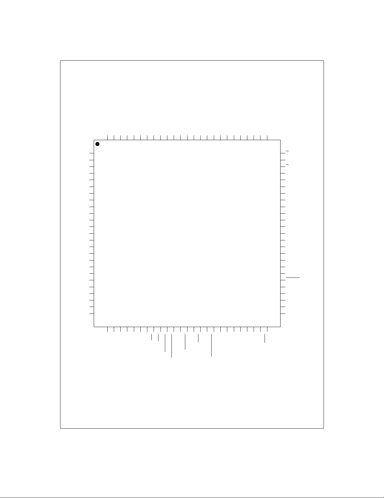
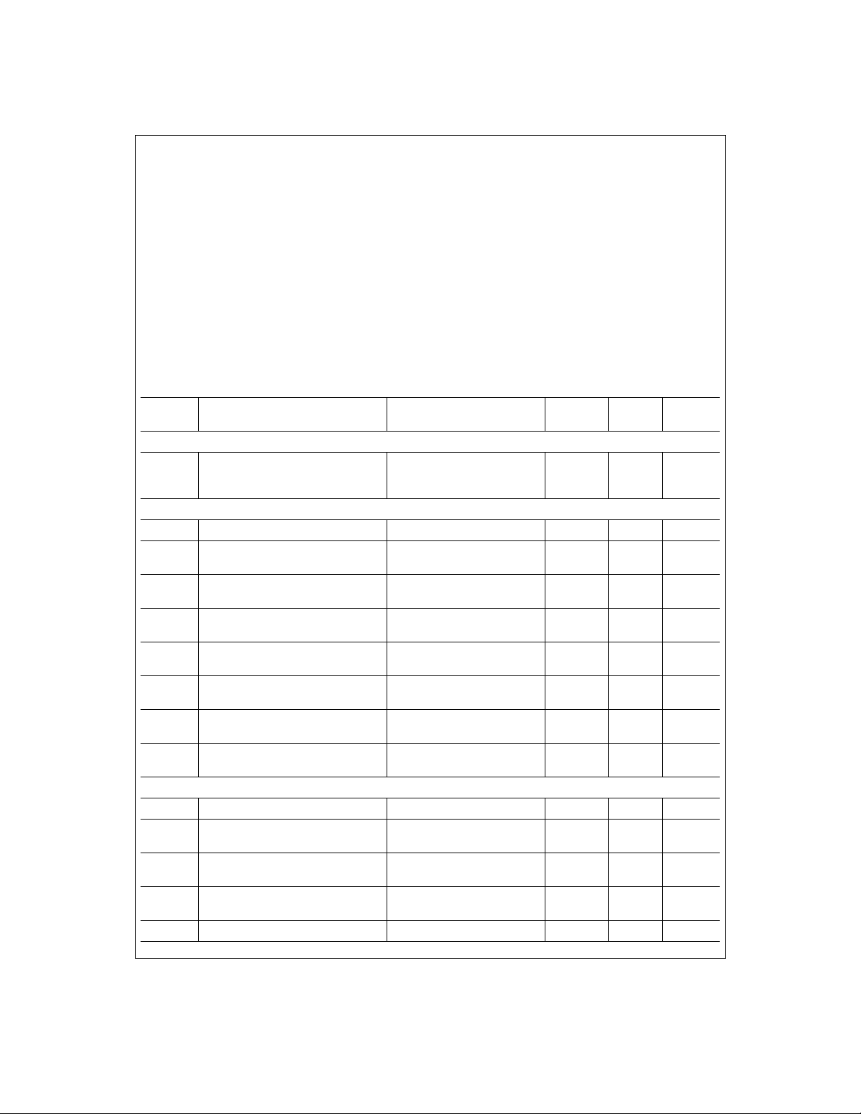
Connection Diagram
GND
V
DGND
V
DGND
A0
A1
A2
A3
A4
D I/O
A5
A6
A7
A8
A9
A10
A11
A12
A13
A14
A15
D I/O
A16
A17
DB0
DB1
DB2
CP2
CP1RSø2ø1TR2
VAOSBV
REF HI SENSEVREF HI FORCE
TR1
AGND
OSGV
REF MID SENSEVREF MID FORCE
OSRV
REF LO SENSEVREF LO FORCEVBANDGAP
AGND
VASENSE
SENSEBSENSEATEST
100999897969594939291908988878685848382818079787776
1
2
3
4
5
6
7
I/O
8
9
10
11
12
13
14
LM9830VJD
15
16
17
18
19
20
I/O
21
22
23
24
25
75
74
73
72
71
70
69
68
67
66
65
64
63
62
61
60
59
58
57
56
55
54
53
52
51
B
B
A
A
CLK_SEL
DGND
I/O
V
D I/O
CMODE
LAMP
B
LAMP
G
LAMP
R
MISC I/O #2
MISC I/O #1
PSENSE #2
PSENSE #1
DGND
SRAM
V
SRAM
CRYSTAL OUT
CRYSTAL IN
LATCH
NC
TRISTATE
SELECT
PE
BUSY
26 27 28 29 30 31 32 33 34 35 36 37 38 39 40 41 42 43 44 45 46 47 48 49 50
DB3
DB4
DB5
DB6
DB7
V
D
RD
DGND
WR
STROBE
AUTOFEED
D0
ERROR
10
D1
D3
V
D I/O
I/O
D4D5D6
D7
ACK
D2
INIT
DGND
SELECT IN
http://www.national.com
Page 11
Pin Descriptions
CCD Driver Signals
ø1 Digital Output. CCD/ CIS clock signal, phase
ø2 Digital Output. CCD clock signal, phase 2.
RS Digital Output. Reset pulse for the CCD.
CP1 Digital Output. Clamp pulse for the CCD.
CP2 Digital Output. Clamp pulse for the CCD.
TR1, TR2 Digital Outputs. Transfer pulses for the
1.
CCD(CIS).
Analog I/O
OSR, OSG,
OS
B
V
REF LO FORCE,
V
REF LO SENSE
V
REF MID FORCE ,
V
REF MID SENSE
V
REF HI FORCE,
V
REF HI SENSE
V
BANDGAP
Analog Inputs. These in puts (for Red, Green,
and Blue) shou ld be tied to th e sensor’s output signal through DC blocking capacitors.
Analog Output/Input . Conne ct V
V
monolithic capacit or.
Analog Output/Input. Connect V
to V
0.05µF monolithic capacitor.
Analog Output/Inp ut. Connect V
V
monolithic capacit or.
Analog Output. Bypass to AGND with a
0.05µF monolithic capacitor.
and bypass to AGND with a 0.05µF
REF LO IN
REF MID IN
REF HI IN
and bypass to AGND with a
and bypass to AGND with a 0.05µF
REF LO OUT
REF MID OUT
REF HI OUT
General Digital I/O
CRYSTAL IN Digital Input. This is the 50MHz (typical) mas-
CRYSTAL OUT Digital Output. Used with CRYSTAL IN and an
CLK_SEL Digital Input. Should be tied to DGND for
ter system clock.
external crystal to form a crystal oscillator.
operation with an external cry stal. To use an
external TTL or CMOS clock source, tie
CLK_SEL to V
CRYSTAL OUT pin.
and driv e th e c lock into t h e
D I/O
PC I/O
D0 (LSB) -D7
(MSB)
STROBE
AUTOFEED
SELECTIN
INIT
ACK
BUSY Digital Output.
PE Digital Output.
SELECT Digital Output.
ERROR
Digital Inputs/Outputs. This is the 8 bit d ata
path between the LM9830 and the host computer.
Digital Input. WR signal in µP Mode.
Digital Input. RD signal in µP Mode.
Digital Input. ALE signal in µP Mode.
Digital Input. CS signal in µP Mode.
Digital Output.
Digital Output.
Printer Passthrough
TRISTATE Digital Output. Low when in printer
LATCH
passthrough mode, high when the LM9830 is
active. Low when no power is app lied to the
LM9830.
Digital Output. High when in printer
passthrough mode, low when th e LM9830 is
active. Tri-state when no power is applied to
the LM9830.
Stepper Motor I/O
A, B, A, B Digital Outputs. Pulses to stepper motor.
,
Analog Inputs. Current sensing for PWM
winding current control.
Analog Input. Ground sense input for PWM
winding current control.
Scanner Support I/O
Digital Inputs. Programmable, used for sensing paper, front panel switches, etc.
Digital Inputs/Outputs. Programmable, used
for front panel switches, status LEDs, etc.
Digital Outputs. Used to control R, G, and B
LEDs of single output CIS, as well as bright-
B
ness of CCFL.
to
to
SENSE
A
SENSE
B
SENSE
GND
PSense #1,
PSense #2
Misc I/O #1,
Misc I/O #2
,
LAMP
R
LAMP
, LAMP
G
External RAM I/O
DB0 (LSB) DB7 (MSB)
A0-A17 Digital Outputs. Add ress pins for up to 256k
RD
WR
Digital Inputs/Outputs. This is the 8 bit data
path between the external RAM and the
LM9830.
bytes external RAM.
Digital Output. Read signal to external RAM.
Digital Output. Write signal to external RAM.
Communication Mode
CMODE Digital Input. Tie to DGND to operate in paral-
lel port mode, or to V
processor c ompatible mode.
D I/O
Test
TEST Analog Output. This pin can be used to view
the Sample Signal, Sample Reference, and
Clamp Signals.
Analog Power Supplies
V
A
AGND This is the ground ret urn for the analog su p-
This is the positive supply pin for the analog
supply. It should be connected to a voltage
source of +5V and bypassed to AGND with a
0.1µF monolithic c apacitor in parallel with a
10µF tantalum capacitor.
ply.
to operate in micro-
11
http://www.national.com
Page 12

Digital Power Supplies
V
D
DGND This is the ground return for V
V
D I/O
DGND
I/O
V
SRAM
DGND
SRAM
This is the positive supply pin for the
LM9830’s digital circuitry. It should be connected to a voltage source of +5V and
bypassed to DGND with a 0.1µF monolithic
capacitor.
.
D
This is the positive supply pin for the
LM9830’s external I/O. It should be connected
to a +5V voltage source and bypassed to the
closest DGND
capacitor.
This is the ground return for V
pin with a 0.1µF mo nolithic
I/O
.
D I/O
This is the positive supply pin for the
LM9830’s internal SRAM sense amplifiers
and crystal o scillator. It should be connected
to a +5V voltage source and bypassed to
DGND
This is the ground return for V
with a 0.1µF monolithic capacitor.
SRAM
D SRAM
.
Other
NC Do Not Connect. This pin should be left float-
ing.
12
http://www.national.com
Page 13
LM9830 Register Listing
(Registers in bold boxes are reset to t hat value on power-up. All register addre sses are in hexadec imal. All other numbers
are decimal unless otherwi se noted.)
Address Function
IMAGE BUFFER (READ ONLY)
00 Pixel (Image) Data nnnnnnnnOne byte of image data.
STATUS REGISTERS (READ ONLY)
01 Image Data Available In Buffer nnnnnnnn
Paper Sensor #1 State
If this input is edge sensitive, reading this
Status Register will clear it.
Paper Sensor #2 State
If this input is edge sensitive, reading this
Status Register will clear it.
Misc I/O #1 State
If this input is edge sensitive, reading this
Status Register will clear it.
Misc I/O #2 State
02
If this input is edge sensitive, reading this
Status Register will clear it.
Pause
This bit indicates whether or not the scanner
is currently paused due to a buffer full
condition.
Powerdrop
This bit is used to detect if the power supply
has dipped below 3V since the last time this
register was read. Reading this register
clears this bit.
DATAPORT REGISTERS
DataPort Target
DataPort Target Color (Note: If using 1
03
Channel Mode A, the color for the gamma
table is selected by register 26, bits 3 and 4,
not this register)
04 DataPort Address - MSB
05 DataPort Address - LSB aaaaaaaa
06 DataPort nnnnnnnn
D7D6D5D4D3D2D1D
0Normal State
1
0
1
R
/Waaaaa
0
n kbytes of image data available
(always read this register twice to make sure its value
was not changing while it was being read)
0False
1True
0False
1True
0False
1True
0False
1True
The scanner entered the pause/reverse cycle during
the processing of this line.
False: Power has not dipped below 3V since the last
time this register was read
True: Power
the register was read
0 Gamma Lookup Table
1 Offset/Gain Coefficient Data (external SRAM)
00 Red
01 Green
10 Blue
11 N/A
Address of location to be read/written to.
a = 0 to 1023 for gamma tables,
0 to 2729 for Offset/Gain Coefficient Data (300dpi),
0 to 5459 for Offset/Gain Coefficient Data (600dpi).
Addresses greater than these are illegal.
Bit D5 of register 4 indicates whether next operation
will be a Read (D5=1) or a Write (D5=0)
Data to be read from or written to the address of the
currently selected Dataport Target. The DataPort
Address is automatically incremented whenever one
(Gamma) or two (Offset/Gain Coefficient Data) bytes
are read from or written to this register.
has
dipped below 3V since the last time
Value
13
http://www.national.com
Page 14
Address Function
COMMAND REGISTER
Command Register
This regis t er i s use d t o s tart an d e nd a s ca n.
It is also used to home the sensor in a
flatbed scanner or eject the image in a
sheetfed scanner.
07
Standby
When this bit is set the crystal oscillator
continues to run but all internal clock signals
are frozen. The analog circuitry is turned off
to reduce power consumption.
Reset
(Host mu st write a 1 then a 0 to enter
and exi t the reset state)
MASTER CLOCK DIVIDER
MCLK Divider
This register sets the master clock frequency
for the entire scanner.
08
f
MCLK
f
ADC
= f
= f
CRYSTAL
MCLK
/MCLK_Divider
/8
HORIZONT AL RESOLUTION AND DATAMODE SETTINGS
Horizontal DPI Divider
This register determines the horizontal
resolution of the scan.
Scan resolution = Optical resolution divided
by the Horizontal_DPI_Divider.
Pixel Packing
This register determines how many bits in
each byte of data are transmitted to the host
when DataMode = 0
DataMode
When DataMode = 0, the pixel data is fully
processed, going through the Offset,
09
Shading, Horizontal DPI Adjust, Gamma,
and Pixel Packing blocks.
D7D6D5D4D3D2D1D
0
Idle - Stops motor (A, B, A
completes current line of data (if scanning).
00
Note: CCD/CIS clocks continue clocking.
High Speed Forward - Moves motor forward at a
01
speed determined by the Fast Feed Step Size
(registers 48 and 49).
High Speed Reverse - Moves motor backward at a
10
speed determined by the Fast Feed Step Size
(registers 48 and 49).
Start Scan - Resets the LM9830’s data pointers and
11
starts an image scan.
0 Operating
1 Low Power Standby Mode
0 Normal Operation
1 Resets the LM9830
000000÷1.0
000001÷1.5
000110÷4
aaaaaa÷ ((aaaaaa/2)+1)
111110÷32.0
111111÷32.5
000÷1
001÷1.5
010÷2
011÷3
100÷4
101÷6
110÷8
111÷12
0 0 1 bit/pixel (1 bit grayscale/3 bit color)
0 1 2 bits/pixel (2 bit grayscale/6 bit color)
1 0 4 bits/pixel (4 bit grayscale/12 bit color)
1 1 8 bits/pixel (8 bit grayscale/24 bit color)
0
1, 2, 4, or 8 bit image data,
as determined by the Pixel Size setting.
Value
, B = 0),
When DataMode = 1, 10 bit data is extracted
following the Horizontal DPI Adjust stage.
Gamma and any other post processing must
be done by the host.
When DataMode = 1, Horizontal DPI Adjust
= 0, and the Offset and Gain coefficients are
set to 0, the 12 bit data straight from the
ADC is transmitted. Offset, Shading,
Gamma and any other post processing must
be done by the host.
10 bit image data - sent in 2 bytes:
X X X X 9 8 7 6- 5 4 3 2 1 0 X X
1
12 bit image data - sent in 2 bytes:
X X X X 11 10 9 8 - 7 6 5 4 3 2 1 0,
Horizontal DPI Divider = 0.
14
http://www.national.com
Page 15

Address Function
RESERVED
Reserved
0A
SENSOR CONFIGURATION
Input Signal Polarity
CDS On/Off
Standard/Even Odd Sensor
0B
Sensor Resolution
(used only for SRAM coefficient allocation)
Line Skipping Color Phase Delay
Part of the “n out of m” function, consisting of
registers 0B (bits 4-7) 44, 45 (bit 5), and 5A.
SENSOR CONTROL SETTINGS
Ø1 Polarity
Ø2 Polarity
RS Polarity
CP1 Polarity
0C
CP2 Polarity
TR1 Polarity
TR2 Polarity
Ø1 Active/Off
Ø2 Active/Off
RS Active/Off
CP1 Active/Off
0D
CP2 Active/Off
TR1 Active/Off
TR2 Active/Off
Number of TR Pulses
TR Pulse Duration
0E
TR-Ø1 Guardband Duration
Optical Black Clamp Start
0F
Optical Black Clamp End
10
Reset Pulse Start
11
Reset Pulse Stop
12
CP1 Pulse Start
13
CP1 Pulse Stop
14
CP2 Pulse Start
15
CP2 Pulse Stop
16
Reference Sample Position
17
Signal Sample Position
18
D7D6D5D4D3D2D1D
0
Value
00000000Write 00 to this register
0 Negative (CCD Sensor)
1 Positive (CIS Sensor)
0 CDS Off
1 CDS On
0 Standard (1 pixels per Ø period)
1 Even/Odd (2 pixels per Ø period)
0 300 dpi (pixels < 2731)
1 600 dpi (2730 < pixels < 5461)
n n n n n lines, n = 0-15
0Positive
1 Negative
0Positive
1 Negative
0Positive
1 Negative
0Positive
1 Negative
0Positive
1 Negative
0Positive
1 Negative
0Positive
1 Negative
0 Off
1Active
0 Off
1Active
0 Off
1Active
0 Off
1Active
0 Off
1Active
0 Off
1Active
0 Off
1Active
01 TR Pulse
12 TR Pulses
nnnnn+1 pixel periods (1-16)
n n n n n pixel periods (0-15)
nnnnn
nnnnn
nnnnn
nnnnn
nnnnn
nnnnn
nnnnn
nnnnn
nnnnn
nnnnn
pixel rate: n=0-23, line rate: n=0-7 MCLKs from Ø1 edge
pixel rate: n=0-23, line rate: n=0-7 MCLKs from Ø1 edge
pixel rate: n=0-23, line rate: n=0-7 MCLKs from Ø1 edge
pixel rate: n=0-23, line rate: n=0-7 MCLKs from Ø1 edge
pixel rate: n=0-23, line rate: n=0-7 MCLKs from Ø1 edge
pixel rate: n=0-23, line rate: n=0-7 MCLKs from Ø1 edge
pixel rate: n=0-23, line rate: n=0-7 MCLKs from Ø1 edge
pixel rate: n=0-23, line rate: n=0-7 MCLKs from Ø1 edge
pixel rate: n=0-23, line rate: n=0-7 MCLKs from Ø1 edge
pixel rate: n=0-23, line rate: n=0-7 MCLKs from Ø1 edge
15
http://www.national.com
Page 16

Address Function
CIS TR1 Timing Mode
19
Fake Optical Black Pixels
(for Dyna-type CIS sensors)
RESERVED
Reserved
1A
Reserved
1B
SENSOR PIXEL CONFIGURATION
Optical Black Pixels Start
1C
Optical Black Pixels End
1D
Active Pixels Start - MSB
1E
Active Pixels Start - LSB
1F
Line End - MSB
20
Line End - LSB
21
PIXEL DATA RANGE TO PROCESS
Data Pixels Start - MSB
22
Data Pixels Start - LSB
23
Data Pixels End - MSB
24
Data Pixels End - LSB
25
D7D6D5D4D3D2D1D
00000000Write 00 to this register
00000000Write 00 to this register
nnnnnnnnn pixels (0 - 255)
nnnnnnnnn pixels (0 - 255)
nnnnnn
nnnnnnnn
nnnnnn
nnnnnnnn
nnnnnnn pixels (
nnnnnnnn
nnnnnnn pixels (
nnnnnnnn
0
0 0 Off - use standard CCD Timing
CIS TR1 Timing Mode 1:
01
TR1 pulse = exactly one Ø clock,
starting at rising edge of Ø1
CIS TR1 Timing Mode 2:
10
TR1 pulse = exactly one Ø clock,
TR1 centered around Ø1 high.
11N/A
0 Off: Normal operat ion
On: RS pulse held high during entire Optical Black
1
period
n pixels (10 - 16383)
This is wh ere image data starts coming out of the
sensor, and determines the pixel where offset and
shading correction begins (pixel 0 in the DataPort)
n pixels (0 - 16383)
This selects the pixel count at which the current line is
ended and the next line begins. This determines the
integration time of one line.
Active Pixels Start
This selects the start of the range of pixels transmitted
to the PC. This value must be >=
Data Pixels Start
This selects the end of the range of pixels transmitted
to the PC. This value must be <= [
Value
- [
- 16383)
Active Pixels Start
Line End
- 20])
Line End
- 20]
16
http://www.national.com
Page 17

Address Function
COLOR MODE SETTINGS
AFE Operation
3 Channel or 1 Channel
1 Channel Mode A Channel Color
(1 Channel Mode B always uses the
26
Blue Channel)
(=TR1) position
TR
RED
(3 Channel Line Rate Mode only)
TR
(=TR2) position
GREEN
(3 Channel Line Rate Mode only)
TR
(=CP2) position
BLUE
(3 Channel Line Rate Mode only)
Integration Time Adjust
drop rate)
(TR
RED
(3 Channel Line Rate Mode only)
Integration Time Adjust
GREEN
drop rate)
(TR
27
(3 Channel Line Rate Mode only)
Integration Time Adjust
drop rate)
(TR
BLUE
(3 Channel Line Rate Mode only)
RESERVED
Reserved
28
D7D6D5D4D3D2D1D
0
Value
0003 Channel Pixel Rate Color
0013 Channel Line Rate Color
1001 Channel Mode A (1 Channel Grayscale)
1011 Channel Mode B (1 Channel Line Rate Color)
00 Red
01 Green
10 Blue
11 N/A
0 1st TR pulse position (inside Ø1 high)
1 2nd TR pulse position (inside Ø1 low)
0 1st TR pulse position (inside Ø1 high)
1 2nd TR pulse position (inside Ø1 low)
0 1st TR pulse position (inside Ø1 high)
1 2nd TR pulse position (inside Ø1 low)
0 0 Do not drop any TR
01Drop 1 TR
10Drop 2 TR
11N/A
RED
RED
0 0 Do not drop any TR
0 1 Drop 1 TR
1 0 Drop 2 TR
11 N/A
GREEN
GREEN
0 0 Do not drop any TR
0 1 Drop 1 TR
1 0 Drop 2 TR
11 N/A
BLUE
BLUE
pulses
RED
pulse (double integration time)
pulses (triple integration time)
pulses
GREEN
pulse (double integration time)
pulses (triple integration time)
pulses
BLUE
pulse (double integration time)
pulses (triple integration time)
00000000Write 00 to this register
17
http://www.national.com
Page 18

Address Function
D7D6D5D4D3D2D1D
ILLUMINATION SETTINGS
Illumination Mo de
Controls the function of the 3 LAMP outputs,
, LAMPG, and LAMP
LAMP
R
B
Mode 0 is the Off/Reset state.
Mode 1 is typically used for CCFL lamps.
29
Mode 2 is for color scanning with tri-color
LEDs.
Mode 3 is for grayscale scanning with tricolor LEDs.
PWM - MSB
LAMP
2A
(Illumination Mode 1)
LAMP
LAMP
2C
LAMP
2D
LAMP
2E
LAMP
2F
LAMP
30
LAMP
31
LAMP
32
LAMP
33
LAMP
34
LAMP
35
LAMP
36
LAMP
37
G
PWM - LSB
G
On - MSB
R
On - LSB
R
Off - MSB
R
Off - LSB
R
On - MSB
G
On - LSB
G
Off - MSB
G
Off - LSB
G
On - MSB
B
On - LSB
B
Off - MSB
B
Off - LSB
B
(Illumination Mode 1) nnnnnnnn
nnnnnnn pixels (1 - 16384)
nnnnnnnn
nnnnnnn pixels (1 - 16384)
nnnnnnnn
nnnnnnn pixels (1 - 16384)
nnnnnnnn
nnnnnnn pixels (1 - 16384)
nnnnnnnn
nnnnnnn pixels (1 - 16384)
nnnnnnnn
nnnnnnn pixels (1 - 16384)
nnnnnnnn
STATIC OFFSET AND GAIN SETTINGS FOR ANALOG FRONT END
Static Offset (Red)
38
Static Offset (Green)
39
Static Offset (Blue)
3A
Static Gain (Red)
3B
Static Gain (Green)
3C
Static Gain (Blue)
3D
0nnnnnOffset = +n*9.3mV, n = 0 to 31
1nnnnnOffset = -n*9.3mV , n = 0 to 31
0nnnnnOffset = +n*9.3mV, n = 0 to 31
1nnnnnOffset = -n*9.3mV , n = 0 to 31
0nnnnnOffset = +n*9.3mV, n = 0 to 31
1nnnnnOffset = -n*9.3mV , n = 0 to 31
0nnnnnGain = 0.93 + 0.067*n (V/V), n = 0 to 31
1nnnnnGain = 3(0.93 + 0.067*n) (V/V), n = 0 to 31
0nnnnnGain = 0.93 + 0.067*n (V/V), n = 0 to 31
1nnnnnGain = 3(0.93 + 0.067*n) (V/V), n = 0 to 31
0nnnnnGain = 0.93 + 0.067*n (V/V), n = 0 to 31
1nnnnnGain = 3(0.93 + 0.067*n) (V/V), n = 0 to 31
0
00
01
10
11
nnnn
Value
LAMP
= LAMPG = LAMPB = 0V
R
(Power-On/Reset Default)
Illumination Mode 1 - LAMP
every line, with their on and off points controlled by
the Pixel Counter settings. LAMP
continuous PWM pulse stream. (Figure 28)
LAMP
and/or LAMPB may be set to stay on or off at
R
all times by setting the LAMP Off or LAMP On settings
and LAMPB turn on
R
Output is
G
(registers 2C-37) greater than the Line End value
(registers 20 and 21).
Illumination Mode 2 - LAMP
on sequentially at the line rate, with their on and off
, LAMPG, LAMPB turn
R
points controlled by Pixel Counter settings. (Figure
29)
Illumination Mode 3 - LAMP
on every line, with their on and off points controlled by
, LAMPG, LAMPB turn
R
the Pixel Counter settings. (Figures 30 and 31)
LAMP
output is a PWM pulse stream. Duty cycle is
G
n/4095. Clock for counter is CRYSTAL IN, giving max
output frequency of 12.2kHz for f
CRYSTAL IN
This selects the pixel count at which the LAMP
output goes high (if programmed)
This selects the pixel count at which the LAMP
output goes low (if programmed)
This selects the pixel count at which the LAMP
output goes high (if programmed)
This selects the pixel count at which the LAMP
output goes low (if programmed)
This selects the pixel count at which the LAMP
output goes high (if programmed)
This selects the pixel count at which the LAMP
output goes low (if programmed)
= 50MHz.2B
R
R
G
G
B
B
18
http://www.national.com
Page 19

Address Functio n
DIGITAL PIXEL RATE OFFSET AND GAIN SETTINGS
Multiplier Gain Range
Smaller gain ranges provide finer control.
Larger gain ranges correct for larger shading
errors.
Offset/Gain data format
3E
Multiplier Coefficient Source
Offset Coefficient Source
Fixed Offset Coefficient
3F
Fixed Multiplier Coefficient - MSB
40
Fixed Multiplier Coefficient - LSB
PARALLEL PORT SETTINGS
Communicati on Mode
(for reading data from any of the LM9830’s
registers)
Note: This register must be set
appropriately before data can be read
42
from the LM9830!
Parallel Port Output Driver Current
(I
and IOH can be used to calculate rise
OL
and fall times into the load capacitance:
rise/fall time approximately equals 5V*C/i)
EXTERNAL SRAM SETTINGS
External SRAM Size
SRAM Interface Output Driver Current
and IOH can be used to calculate rise
(I
OL
and fall times into the load capacitance:
rise/fall time approximately equals 5V*C/i)
SRAM Bandwidth (8 Bit Data Mode)
43
8 slot mode should always be used to
maximize performance. If the external
SRAM is to slow to meet the t
requirement, the slower 4 SRAM
RD SETUP
accesses/ADC clock mode may be used.
Scanning Duplex (10/12 bit Data Mode)
Full Duplex mode should always be used to
maximize scan speed. If the external SRAM
is to slow to meet the t
the slower Half Dupl ex mode may be used.
RD SETUP
requirement,
D7D6D5D4D3D2D1D
0
0 0 1.5:1 (33%)
0 1 2.0:1 (50%)
1 0 3.0:1 (66%)
1 1 Bypass Multiplier
0 6 bits offset/10 bits gain
1 8 bits offset/8 bits gain
0 Configura tion Register 3F (Fixed)
1 External SRAM
0 Configuration Register 40 and 41 (Fixed)
1 External SRAM
nnnnnnnn
Fixed Offset to use for calibration - 2MSBs are
assumed to be 0 if using 6 bit offset format
n n Fixed Gai n to use f o r cal ibr at ion - 2L SBs ar e ass ume d
nnnnnnnn
to be 0 if using 8 bit gain format41
0 8 bit Bidirectional/EPP
1 4 bit Nibble
00 I
01 I
10 I
11 I
= 5mA, IOH = -6mA
OL
= 7mA, IOH = -9mA
OL
= 9mA, IOH = -12mA
OL
= 15mA, IOH = -21mA
OL
0 0 64 kbytes (not recommended for 600dpi scanners)
0 1 128 kbytes
1 0 256 kbytes
11N/A
00 I
01 I
10 I
11 I
= 3.5mA, IOH = -4mA
OL
= 6mA, IOH = -7.5mA
OL
= 12mA, IOH = -17mA
OL
= 21mA, IOH = -32mA
OL
0 4 SRAM accesses/ADC clock
1
0
1
8 SRAM accesses/ADC clock
must be 25MHz or lower)
(f
MCLK
Full Duplex- Can transmit data while scanning
must be 25MHz or lower)
(f
MCLK
Half Duplex - Can only transmit data when buff er is full
or scan has been stopped
Value
19
http://www.national.com
Page 20

Address Function
STEPPER MOTOR CONTROL SETTINGS 1
n (Line Skipping)
44
Part of the “n out of m” function, consisting of
registers 0B (bits 4-7) 44, 45 (bit 5), and 5A.
Full/Microstepping
Current Sensing Phases
= 0 for fullstepping
= 1 for microstepping
Stepper Motor Pha se A Polarity
45
Stepper Motor Pha se B Polarity
, and B stepper motor status
A, B, A
Line Skipping Phase
Part of the “n out of m” function, consisting of
registers 0B (bits 4-7) 44, 45 (bit 5), and 5A.
Scanning Step Size - MSB
46
Scanning Step Size - LSB
Fast Feed Step Size - MSB
48
Fast Feed Step Size - LSB
Fullsteps to Skip at Start of Scan - MSB
4A
Fullsteps to Skip at Start of Scan - LSB
Fullsteps to Scan after Paper Sensor #2
4C
trips -MSB
Fullsteps to Scan after Paper Sensor #2
trips -LSB
Pause scanning, stop/reverse motor
4E
Resume scanning, start motor
4F
Full steps to reverse when buffer is full
50
Acceleration Profile (stopped)
Acceleration Profile (25%)
51
Acceleration Profile (50%)
Default Phase Difference - MSB
52
Default Phase Difference - LSB
Lines to Process After Pause Scan Signal
54
Lines to Discard after Resume Scan
Signal
Kickstart Steps
55
Hold Current Timeout
Stepper Motor PWM Frequency
56
Stepper Motor PWM Set Duty Cycle
57
(fullstepping mode) nnnMotor gets maximum current for first n (0-7) full steps
D7D6D5D4D3D2D1D
tttttttt
0
1
0 Red sensor data arrives before Green sensor
1 Blue sensor data arrives before Green sensor
nnnnnnThe step size of one microstep while scanning, in
nnnnnnnn
nnnnnnThe step size of one microstep while fast feeding, in
nnnnnnnn
nnnnnnWhen scan starts, paper is fed forward n full steps (0 -
nnnnnnnn
nnnnnnAdds a delay of n (0-16383) full steps between when
nnnnnnnn
nnnnnnnnPause scan when buffer is n kbytes full
nnnnnnnnResume scan when buffer is n kbytes full
nnnnnnn (0-63) full steps (0 = do not reverse)
n n n (0-3) full steps at 50% speed
nnnnnnnnUsed to calculate when motor resumes after reversing
nnnnnnnn
nnn
nnnnn Full step time units (1-31), 0 = no hold current
nnnnnnnn
nnnnnn= n/64 (default = 0)
0
n lines saved in SRAM for every m lines (register 5A)
scanned, function bypassed if register value = 0.
n (lines saved per m lines scanned) = 256 - t
t = 256 - n
If t = 0 then function is bypassed
0 Full Step Mode
1 MicroStepping Mode
1 Phase - No microsteppi ng, just kickstart/stop
0
functions
1 2 Phases - necessary for microstepping
0
Positive (A/B/A
1
0
1
n n n (0-3) full steps at 25% speed
Negative (A/B/A
Positive (A/B/A
Negative (A/B/A
A, B, A
, and B output pins in Tri-State
A, B, A
, and B output pins active
units of pixel periods (minimum 2).47
units of pixel periods (minimum 2).49
16383) at highest speed. For “zooming” in flatbeds4B
Paper Sensor #2 trips and when the scanning bit is
reset, terminating the scan/motor movement.4D
n n n (0-3) full step time units pause while stopped
and stopping. 1 < n < 6553553
n (0-7) lines. This only applies if the motor doesn’t
nnn
reverse (reverse steps = 0).
n (0-7) lines. This only applies if the motor doesn’t
reverse (reverse steps = 0).
Should be set to same value as bits 0-2.
=CRYSTAL IN/(4*n) (0 < n < 256)
=CRYSTAL IN/(4*256) (n = 0)
Value
/B Output high = winding energized)
/B output low = winding energized)
/B Output high = winding energized)
/B output low = winding energized)
20
http://www.national.com
Page 21

Address Function
PAPER SENSOR SETTINGS
Paper Sensor #1 Polarity
Paper Sensor #1: Level/Edge sensitive
Paper Sensor # 1: Stop Scan
Paper Sensor #2 Polarity
58
Paper Sensor #2: Level/Edge sensitive
Paper Sensor # 2: Stop Scan
MISC I/O PIN SETTINGS
Misc I/O #1: Input or Output
Misc I/O #1: Polarity
(if configured as an input)
Misc I/O #1: Level/Edge sensitive
(if configured as an input)
Misc I/O #1: Output State
(if configured as an output)
59
Misc I/O #2: Input or Output
Misc I/O #2: Polarity
(if configured as an input)
Misc I/O #2: Level/Edge sensitive
(if configured as an input)
Misc I/O #2: Output State
(if configured as an output)
STEPPER MOTOR CONTROL SETTINGS 2
m (Line Skipping)
5A
Part of the “n out of m” function, consisting of
registers 0B (bits 4-7) 44, 45 (bit 5), and 5A.
D7D6D5D4D3D2D1D
0
1
0
1
0 The Misc I/O #2 pin is configured as an input.
1 The Misc I/O #2 pin is configured as an output.
0 A low input on Misc I/O #2 is True
1 A high input on Misc I/O #2 is True
0
1
0
1
mmmmmmmm
0
0 A low input on Paper Sensor #1 is True
1 A high input on Paper Sensor #1 is True
Level sensitive: Paper Sensor #1 State bit (in Status
0
Register) is set to a 1 if Paper Sensor #1 is currently
True.
Edge sensitive: Paper Sensor #1 State bit (in Status
1
Register) is set to a 1 if Paper Sensor #1 has been
True since the last time the Status Register was read.
Transitions on Paper Sensor #1 will not clear the
0
scanning bit.
A False - to - True transition on Paper Sensor #1 will
1
0 A low input on Paper Sensor #2 is True
1 A high input on Paper Sensor #2 is True
0
1
clear the Command Register and stop the scan.
Level sensitive: Paper Sensor #2 State bit (in Status
Register) is set to a 1 if Paper Sensor #2 is currently
True.
Edge sensitive: Paper Sensor #2 State bit (in Status
Register) is set to a 1 if Paper Sensor #2 has been
True since the last time the Status Register was read.
Transitions on Paper Sensor #2 will not clear the
scanning bit.
A False - to - True transition on Paper Sensor #2 will
clear the Command Register and stop the scan (after
the number of lines specified in the
after Paper Sensor #2 trips
0 The Misc I/O #1 pin is configured as an input.
1 The Misc I/O #1 pin is configured as an output.
0 A low input on Misc I/O #1 is True
1 A high input on Misc I/O #1 is True
Level sensitive: Misc I/O #1 State bit (in Status
0
Register) is set to a 1 if Misc I/O #1 is currently True.
Edge sensitive: Misc I/O #1 State bit (in Status
1
Register) is set to a 1 if Misc I/O #1 has been True
since the last time the Status Register was read.
The output of the Misc I/O #1 pin will be a logic low
(0V).
The output of the Misc I/O #1 pin will be a logic high
(5V).
Level sensitive: Misc I/O #2 State bit (in Status
Register) is set to a 1 if Misc I/O #2 is currently True.
Edge sensitive: Misc I/O #2 State bit (in Status
Register) is set to a 1 if Misc I/O #2 has been True
since the last time the Status Register was read.
The output of the Misc I/O #2 pin will be a logic low
(0V).
The output of the Misc I/O #2 pin will be a logic high
(5V).
n lines (register 44) saved in SRAM for every m lines
scanned. m = 1 to 255.
If m = 0 then function is bypassed
Value
Fullsteps to Scan
register).
21
http://www.national.com
Page 22

Address Function
TEST MODE SETTINGS
Reserved
5B
ADC Output Code - MSB
5C
ADC Output Code - LSB
Reserved
Offset Subtractor Input Select
5E
CDS Signal
Reserved
5F-6F
Parallel Port Noise Filter
70
Reserved
71-7F
D7D6D5D4D3D2D1D
00000000Write 00 to this register
nnnnnnnn
00000000
0 The ADC is input to Offset Subtractor
1 Registers 5C and 5D are input to Offset Subtractor
0 Normal Operation
1 CDS signal is output on TEST pin
00000000Write 00 to these registers
01110000Write 70 to this register
00000000Write 00 to these registers
0
nnnnUsed to force the input to the Offset Subtractor
to a known value for digital tests5D
Write 00 to this register for normal operation, modify
bits 5 and 7 as shown below for test modes
Value
22
http://www.national.com
Page 23

Applications Informat ion
pixel
100dpi
p
n-2pn-1pn
++
3
-------------------- ----------------------- -=
1.0 THEORY OF OPERATION
1.1 Overview
A scanner is composed of many different but tightly interconnected blocks (the analog fro nt end a nd ADC, sensor c lock generation, stepper motor con trol, data buffering, parallel por t I/O,
and others).
1.2 Signal Processing Overview
1.3 Scanner Support Functions Overview
2.0 Signal Processing Operation
2.1 ADC
The ADC is a 6MHz 12 bit pipelined architecture.
2.2 Pixel Rate Offset Correction Block
Two bytes are used to store the pixel rate offs et and gain co efficients for each pixel. For CCDs, the split is usually 6 bits for offset
and 10 bits for gain. For som e CIS sensors w ith unusually large
offsets, the offset correction range may be increased by changing
the split to 8 bit s for offset and 8 bits for gai n. This split is determined by a bit in the configuration register.
A digital subtractor subtra cts the 6 (or 8) bit offset word (corresponding to that pixel’s offset error) from each pixel. The LSB of
the offset word is the same size as the 10 bit LSB of the ADC (the
two smallest 12 bit ADC output bits, D1 and D0, are not used with
the offset subtractor). Th e coefficients are stor ed in the external
RAM and accessed at the pixel rate.
The subtractor saturates at 0, i.e. if the coefficient to be subtracted is greater than the ADC o utput code, th e resu lt is an o utput of 0.
2.3 Pixel Rate Gain Correction Block
This is a digital multiplier that multiplies the output word from the
subtractor by a 10 (or 8) bit digital correct ion coefficient corresponding to that pixel’s gain error. The coefficients are st ored in
the external RAM and a ccessed at the pixel rate. When in 8 bit
mode, the 8 bits correspond to the top 8 MSBs of the 10 bit digital
correction coefficient word. Th e 10 bit LSB s o f the inpu t word a re
padded with 0s in 8 bit mode.
The multiplier saturates at 1023, i.e. if the result of the multiplication is greater than 1023, the multiplier output is 1023.
2.4 Pixel Processing Block
2.4.1 Pixel Processing In 8/24 Bit Mode
In the 8 and 10 bit o utput mod es (for 24 and 30 bit c olor scan s),
this stage is where the optical resolution of the sensor is digitally
reduced.
To maximize scanning speed and imag e quality at the popular
resolutions of 400, 300, 200, 150, 100, 75, and 50 dpi, the resolution can be reduced ins ide the scanner, prior to th e gamma correction stage. (Resolu tion in t he ver tic al dir ection is cont rolled by
the stepper motor speed.) This is done by averaging adjacent pixels. For example, to get 100 dpi from a 300dpi optical sensor, you
would average 3 300dpi pixels:
The number of pixels out of the Pixel Processing block is equal to
the integer portion of the number of pixels in to the Pixel Processing block divided by the “Divide By” setting, fro m the table shown
in Figure 11.
Pixels
IN
------------------- ------
OUT
=
INT
Divide By
Pixels
If there are not enough pixels at the end of a lin e to form a complete pixel, the last pixel will be eliminated. For example, if a line
is 35 pixels wide and the Horizontal DPI setting is set to divide by
6, then the output of the Pixel Processing block will be 5 pixels
(the integer portion of 35/6). The last 5 pixels will be discarded,
since 6 pixels would be required to form a new pixel in this mode.
Boost
1V/V or
3V/V
+
+
V
IN
G
Σ
+
V
OS1
B
+
Σ
+
V
OS2
Offset
D
= (((VIN + V
OUT
simplified, with all offsets = 0, this is:
D
OUT
PGA
0.93V/V t o
3V/V
Σ
+
V
DAC
DAC
+ V
OS1)GB
= (VINGB + V
G
PGA
DAC
+
Σ
+
V
OS3
+ V
OS2)GPGA
DAC)GPGA
+ V
12 Bit
ADC
OS1
D
OUT
)C
C
C is a constant that combines the gain error through the AFE, reference voltage variance, and analog voltage
to digital code conversion into one constant. Ideally, C = 2048 codes/V (4096codes/2V). Manufacturing toler-
ances widen the range of C. See Electrical Specifications
Figure 10: Analog Front End (AFE) Model
23
http://www.national.com
Page 24

This equation also applies to the divide by 1.5 function.
(X=mask out in software).
Divide
By
DPI
(600 DPI sensor)
DPI
(300 DPI sensor)
1 600 300
1.5 400 200
2 300 150
3 200 100
4 150 75
6 100 50
875 37.5
12 50 25
Figure 11:
Decreasing Horizontal Resolution
The output of this stage is sen t through the gamma and pixel
packing stages, resulting in output data for matted as shown in
Figure 15.
2.4.2 Pixel Processing 10/30 Bit Mode
Scanning in 10 bit mode (30 bit co lor) supports the Horizontal
DPI Divider function as wel l as the pixel rate shading and offse t
functions. The output dat a is formatted as shown in Figure 12
(X=mask out in software).
76543210 Order
XXXX9876 First Byte
543210XX Second Byte
Figure 12:
10 Bit Mode Pixel Data Format
The software on the host PC must perform any gamma correction
desired.
There are two varia tions on t he 10 and 12 bi t ou tput m odes: Ful l
Duplex and Half Duplex, determined by bit 5 of Configuration
Register 43. In the Fu ll Duplex mode, there are 6 S RAM operations per pixel: offset data read , gain data r ead, pixel MSB wri te,
pixel LSB write, pixel MSB r ead , p ixel LSB re ad) . S in c e t her e are
8 MCLKs per pixel, the writes take 2 MCLK periods and the reads
take 1 MCLK period. T his mode is preferred because it permits
faster scanning, but it requires fast SRAM access.
The Half Duplex mode accommodates slower SRAM. In Half
Duplex mode, the data in the SRA M ca n not be r ead by th e hos t
PC until the buffer is full. Therefore there are two phases to scanning data in the Half Duplex mode. The first is writing pixel data to
SRAM using 4 operations/pixel (offset data read, gain data read,
pixel MSB write, pixel LSB write). In this mode the read and write
cycles will all be 2 MCLKs long. The second phase is reading the
contents of the SRAM and sen ding them to the host PC. This
read operation uses 2 MCLK read cycles/byte.
2.4.3 Pixel Processing: 12/36 Bit Mode
Scanning in 12 bit mo de (36 bit color) can onl y be done at the
optical resolution of the se nsor, and the shading and of fset functions can not be used. The Horizon tal DPI Divide r function must
be set to 1 (register 09, bits 0-2 = 0) to get 12 bit data. The shading and offset functions must a lso be disabled (registe rs 3E, 3F,
40, and 41 all set to 0). The 10 bi t p ixel output from the multiplier
is combined with the 2 12 bit LSBs from the ADC to re create the
12 bit pixel. The output data is formatted as shown in Figure 13
76543210 Order
XXXX111098 First Byte
76543210 Second Byte
Figure 13:
12 Bit Mode Pixel Data Format
The software on the host PC must perform all offset an d shading
correction, horizonta l resolution adju stment, and gamm a correction.
The 12 bit mode uses the same Full or Half Duplex options
described in
2.4.2 Pixel Processing 10/30 Bit Mode
2.5 Gamma Correction Tables
There are 3 ga mma lookup tables for R, G, and B. The input to
the table is the 10 b it pixel data coming from the previous stage
2.4 Pixel Processing Block
(
). The output is the 8 bit gamma corrected pixel data. The tables are therefore 1K bytes x 8 bits in
size. Each gamma table (red, green, and blue) can be loaded with
255
8 Bit Pixel Out
0
0 1023
10MSBs of 12 bit Output
Figure 14:
Gamma Table
any arbitrary user-defined transfer curve.
The gamma ta bles ar e l oa ded t hro ugh the dataport ( see
5.1 The
DataPort: Reading and Wr iting to Gamma, Offset, and Gain
Memory
). In most LM9830 m odes, the DataPort selects which
color (Red, Green or Blue) gamma table will be read from or written to. In 1 Channel Mode A, the on ly gamma table that can be
accessed is the gamma table for the 1 Channel Mod e A color
selected by bits 3 and 4 of register 26.
2.6 Pixel Packing/Thresholding Block
Some scans require only one bit per pixel (“line art” mode), others
may need only 2 or 4 bits/pixel. To increase scanning speed for
lower pixel depths, the LM9830 pa cks the d esire d M S Bs of multiple pixels together, increasing the tran smi ssio n s pee d to the host
by a factor of 2, 4, or 8. Figure 15 shows how the pixels are
Pixel
Depth
76543210
8b7 p
4b7 p0b6 p0b5 p0b4 p0b7 p1b6 p1b5 p1b4 p
b6 p0b5 p0b4 p0b3 p0b2 p0b1 p0b0 p
0
2b7 p0b6 p0b7 p1b6 p1b7 p2b6 p2b7 p3b6 p
1b7 p0b7 p1 b7 p2b7 p3b7 p4b7 p5b7 p6b7 p
Figure 15:
Packing Multiple Pixels Into One Byte
0
1
3
7
packed together for 8, 4, 2, and 1 b it pixel depths. In Figure 15,
“b” indicates the bit po sition (b7 = the m ost significant and b0 =
24
http://www.national.com
Page 25

the least significant bit) of the original 8 bit pixel data, and pn indi-
LPI4C
StepSize
pixels/line
------------------- -------=
cates the original pixel sequence, i.e p
, p1, p2, p3...
0
If there are not enough un packed pixels at the end of a line to
complete the packed byte for transmission, that final byte is not
sent.
The gamma table in
2.5 Gamma Correction Tables
allows the
user to set the thresho ld of each transition for various line ar t or
reduced pixel depth modes.
of the image sen sor, determines the effective ver tical resolution
(Lines Per Inch, or LPI).
The stepper motor is moved forwards and ba ckwards by two signals, A and B, 90° out of phase with each other. The phase for the
forward direction is set in Configuration Register 45.
The A and B signals are either squarewaves (in Full Step Mode,
Figure 16), or a staircase approximation of a sine wave (in
Microstep mode, Figures 18 and 19 ) .
2.7 Line Buffer
The line buffer uses the exter nal SRAM to st ore t he pi xel data a t
the fixed rate and send it back to the PC at a n asynchronous,
unpredictable, and non-constant rate.
This buffer is tightly coupled to the st epper motor (
Motor Controller
), and is responsible for stopping the motor
3.0 Stepper
before the buffer overflows and starting the moto r again as the
buffer nears empty.
If the scanner is generating p ixel data faster than the PC can
acquire it, the line buffer will start to fill up. As the buffer nears
100% full, the scan mu st be paused before it star ts acquiri ng a
line it cannot store becaus e of lack of R AM. Th is Pause Threshold limit (register 4E) is programmable in 1 kbyte increments
between 0 and 255 kbytes but should be no higher than 100 % of
the buffer RAM size minus 1 line of data (for single output CCDs
and CIS) or 3 lines of data (for triple output CCDs and CIS).
When this point is re ached the buffer sends a command to the
stepper motor controller to stop scanning. The remainde r of the
line being processed will continue being processed and be sen t
to the buffer. If the Lines To Process After Pause Scan Signal register (register 54) is greater than 0, then room for these additional
lines need to be added into th e Pause Threshold value calculation.
After a pause, the buffer will now transmit data to the PC until it
hits the Resume Threshold li mit (register 4F), wh ich is also programmable in 1 kbyte increments between 0 and 256kbytes.
When the Resume T hreshold is reache d, the Line Buffer sends
the motor controller a command to resume.
Note that the scanner soft ware on the host PC is resp onsible for
ensuring that the Pause Thresho ld value is low eno ugh to ensure
that any data that comes aft er a pause request (the rest o f the
current line and any s ubsequent lines if register 54 bits 0-2 are
greater than 0) will fit into the SRAM buffer size, which is equal to
SRAM size - COEFFICIENT size.
The pause condi tion i s rea ched w hen the nu mber of bytes in the
buffer is equal to the value in register 4E * 1024. The scan will
resume when the number of bytes in the buffer is equal to (the
value in register 4F * 1024 + 1023).
Since the external SRAM also contains the pixel gain and offset
data (see
2.2 Pixel Rate Offset Correct ion B lock
Rate Gain Correction Block
), the buffer is as large as the SRAM
and
2.3 Pixel
size minus the coefficient storage. Suppor ted SRAM sizes are
64kbyte, 128kbyte, and 256kbyte. Coefficient data always takes
up a total of 16kbytes for 300dpi sensors and 32kbytes for 600dpi
sensors.
A
A
1 full step = 4
microsteps
B
B
Figure 16:
Stepper Motor Waveform - Full Stepping
The LM9830 always counts stepper motor steps in units of
microsteps. A full step is equal to four microsteps. Even when the
LM9830 is in Full Step Mode, it is counting in microsteps, and will
increment the step per motor (generating a f ull step) every four
microsteps.
The microstep Step Size is defined in units of time. These units of
time are pixel period s, as defined i n the hor izontal pixel counter.
In the 3 channel pixel rate input mo de, the pixel period is the
f
/3 (= f
ADC
modes, the pixel period is equa l to f
Size is stored in the
/24). In the 3 channel line rate and 1 channel
MCLK
Scanning Step Size
/3 (= f
ADC
MCLK
configuration register
/24). The Step
as a 14 bit value. During nor mal operation, the stepper motor is
advanced 1 microstep every Step Size pixel periods. The LPI can
be calculated as follows:
Where C = the number of full steps r equired to move the image
one inch, pixels/line is the number of pixel periods it takes to scan
one horizontal line (equivalent to the value stored in the
Line End
registers), and StepSize is the number of pixel periods/microstep
Whenever the stepper motor has been moving and then comes to
a stop, the LM9830 waits for the time s pecified in the Hol d Current Timeout reg ister and th en de- asserts the A, B, A
, and B outputs to cut power to the motor. When the stepper motor is not
scanning or fast-feeding (Command = 00) , A, B, A
, and B are de-
asserted in all stepper modes.
There are two modes of stepper motor operation: fullstepping and
microstepping.
3.1 Full Step Mode
In Full Step Mode th e output i s a pulse stre am, as shown in Fi gure 16. The amplitud e of the puls es is con trolle d by the ou tput of
3.0 Stepper Motor Controller
The stepper motor controller sends a series of pulses to the stepper motor to move the paper past the sensor (sheetfed) or the
sensor past the paper (flatbe d). The speed at which the paper
moves relative to the sensor, combined with the integration time
25
http://www.national.com
Page 26

the 2 bit DAC, shown in Figure 17.
noise generated by the driver transistor turning on.
Scan Mode DAC Voltage
0.5V for number of steps specified in
Starting from
a dead stop
Kickst art Steps
register (0-7). If
register is 0 there is no kickstart
current - movement begins at 0.35V.
Scanning 0.35V
0.125V for number of steps specified
Stopped
in
(0 - 31), 0V after time out. If register
register
Hold Current Timeout
is 0 there is no hold current.
Figure 17:
Full Step Current Control
3.2 MicroStep Mode
Microstepping is a tech nique of driving th e stepper motor with a
staircase approximation of a sine wave, as shown in Figure 18.
This technique maximizes the torque of a given motor, resulting in
a higher maximum speed. In additi on, it increases the reso lution
of the stepper motor. If a stepper motor moves 3.6° per full step,
microstepping can crea te positions inside the 3.6°: 1.8°, 0. 9°, or
0.45°, for example. This increases the maximum vertical resolution of the scanner. Microstepp ing also results in quiet er motor
movement.
A
A
1 microstep
B
B
Figure 18:
Bipolar Microstepping Waveform
The amplitude of th e m icro s tep ped sine wave is contro lled by the
output of the stepper motor DAC (Figure 19). The cu rrent in the
stepper motor winding is measured as a voltage across the sense
resistor, and the transistor drive signals a re pulse width modulated (PWM) to force the average current through the winding
equal to V
PWM, and Register 57 controls the minimum time the driver is on
DAC/RSENSE
. Register 56 controls th e frequenc y of the
every period. Register 57 should be set as short as possible, the
driver only needs to be on long enough to ma sk any transient
DAC A
A
A
DAC B
B
B
Figure 19:
Stepper Motor Waveform - LM9830 Signals
Figure 20 shows the LM983 0’s DAC voltages. The peak current
through the stepper motor winding will be 0.5V/R
index is incremented every microstep (StepSize pixel periods).
SENSE
. The table
Table Code A (B) A (B) DA C Voltage
000N/A
1100.191V
2100.353V
3100.462V
4100.500V
-0 0 0 N/A
-1 0 1 0.191V
-2 0 1 0.353V
-3 0 1 0.462V
-4 0 1 0.500V
Figure 20:
Microstepping Current Control
3.3 Pause Behavior - Non-Reversing Mode
When the
Full Steps to Reverse When Buffer is Full
register is
0, the stepper motor s imply st ops moving wh en the Pause signa l
is received, as s hown in Figure 21 . The line of data currentl y
being processed (section “a” in Figure 21) will continue to be processed and st ored in SRA M. Add iti ona l line s ma y be digi tiz e d and
stored as well, depending on the number programmed in the
Lines to Process After Pause Scan Signal
register (Figure 22).
This value is different for different scanner designs and should be
empirically set t o the value that minimizes the spacial distor tion
created by the motor slowing down and stopping.
TR
abcd
MicroStep
Pulse
Pause
Scanning
Signal
Figure 21:
Stepper Motor Stopping
26
http://www.national.com
Page 27

Value Additional Lines to Store in SRAM
00(a only)
1 1 (a and b)
2 2 (a, b and c)
... ...
77
Figure 22: Lines to Process after Pause Scan Signal
When the Resume Scan signa l is received, the stepper motor
controller waits the appropr iate number of pixel peri ods after the
next TR pulse and then star ts stepping again at th e nor mal rate.
The first new line transmitted is de term ined by the
card After Resume Scan Signal
must be the same as the value in th e
Pause Scan Signal
Value First Line to Transmit After Pause
0b
1c
2d
... ...
7i
Figure 23: Lines to Di scar d Aft er Res ume Scan Si gnal
TR
MicroStep
Pulse
3.4 Pause Behavior - Reversing Mode
Full Steps to Reverse When Buffer is Full
If the
then the Reversing Mode is enabled.
The Reversing Mode eliminates spacial distortion due to the
pausing of a scan. When the Pause Scan signal is received, the
line currently being p rocessed is completed and sto red in RAM
(line “b” in Figure 25). When the scan resumes, ideally the
LM9830 would send out lines “c ” an d after under t he exact same
speed and positional condi tions the scanner was in before the
scan stopped (as indicated by the dotted line in Figure 25).
When the Pause Scan signal is r eceived, the LM9 830 sends out
the remainder of the line currently being read from the CCD (line
b), and stores the offset (in pixel periods) between the last TR
pulse and the last step. It then stops, reverses, stops, and waits
for the Resume Scan signal. Once Resume Scan is asserted, the
motor controller waits for the previously stored num ber of pixels
periods, then star ts moving forward again, m aintaining th e same
phase relationship b etween the TR pulse and th e stepper motor
control signals. The re sult is as if the stepper m otor had never
paused.
register.
Figure 24:
Resume
Scanning
Stepper Motor Resuming
register. The discard value
Lines to Process After
Register
abcd
Signal
Register
Lines to Dis-
register is >0,
TR
MicroStep
Pulse
MicroStep Puls e
(if motor had not
paused)
Stopping, reversing, and resuming forward motion all follow the
curve programmed in the
ister. There are 3 segments (Stopped, 25%, and 50%), and the
number in each re giste r in di ca tes the num ber o f fu l l ste ps to stay
at that acceleration. A value of 0 in di cat es t hat tha t se gme nt is to
be skipped. For example, a value of 0 in all three re gisters would
mean that the motor w ould instantly reverse when the buffer is
full, then instantly stop after going back the specified numb er of
lines.
Speed
Register
Stop
(x = 0 to 3)
25%
(y = 0 to 3)
50%
(z = 0 to 3)
This acceleration profile is us ed any time the motor is started,
stopped, or reversed.
The acceleration profile for stopping, reversing, stopping, and
going forward again is this:
• Full speed forward (1 ste p = #pixels in
register) until the Pause Scanning signal is received.
• 50% speed forward for z steps (1 step = 2* #pixels in
Step Size
• 25% spee d forward for y steps (1 ste p = 4* #p ixels in
Step Size
• Stopped for x microsteps (= #pixels in
ister).
• 25% speed backward for y steps (1 step = 4*#pixels in
ning Step Size
• 50% speed backward for z steps (1 step = 2* #pixels in
ning Step Size
• Full speed backward (1 step = #pixels in
register) for number of steps in the
• 50% speed backward for z steps (1 step = 2* #pixels in
ning Step Size
• 25% speed backward for y steps (1 step = 4*#pixels in
ning Step Size
abcd
Pause
Scanning
Signal
Figure 25:
Figure 26: Acceleration Profile Settings
register)
register)
register)
register)
register)
register)
Reversing - The Goal
Acceleration Profile
DAC output
x = number of full step clocks to wait
before reversing motor.
y = number of full st eps at 25% of fina l
speed. Full step period = 4 full step
clocks.
z = number of full st eps at 50% of fina l
speed. Full step period = 4 full step
clocks.
Steps to Reverse
configuration reg-
Scanning Step Size
Scanning Step Size
Scanning Step Size
e
Scanning
Scanning
reg-
Scan-
Scan-
register
Scan-
Scan-
27
http://www.national.com
Page 28

• Pause d un ti l a Re su m e S can signal is rec ei ved. During th e ho l d
current timeout per iod, the DAC output is held at 0.125V ( the
hold current) for FullStep mode, or the DAC outputs are held as
they were prior to st opping for the microstep mode. A fter the
hold current timeout per iod, output drivers A, B, A
, and B are
deasserted .
• Wait for Resume Scan signal
• Wait for correct number of pixel periods to resync hronize stepper motor w ith sensor timing.
• 25% speed forward for y steps (1 step = 4*#pixels in
Step Size
register)
• 50% speed forward for z steps (1 step = 2* #pixels in
Step Size
• Full speed forward (1 st ep = #pixels in
register).
Scanning Step Size
Scanning
Scanning
register), with TR pu lses synchronize d to same the p osition on
image that they would have been had scanner not stopped.
Lines to Process After Pause Scan Sig nal/Lines to Dis-
The
card After Resume Scan Signal
register is not used in reversing
mode.
are four illumination modes in the LM9830:
Illumination
Mode
0
LAMP
This is the power-on default.
Description
, LAMPG, LAMPB outputs = 0.
R
Scanning with white light:
LAMP
and LAMPB controlled by
1
R
LAMP On/Off pointers in horizontal
pixel counter (as in Mode 3),
LAMP
is a PWM pulse stream
G
Scanning with 3 LEDs in color:
LAMP
turns on for Red lines
2
3
Figure 27:
R
LAMP
turns on for Green lines
G
LAMP
turns on for Blue lines
B
Scanning with 3 LEDs in gray:
LAMP
turns on for all lines
R
LAMP
turns on for all lines
G
LAMP
turns on for all lines
B
Illumination Modes
3.5 Fast Feed Step Size Register
When the motor is being moved quickly (
End/Paper Feed to Beginnin g
Start of Scan
register), the micro step period comes from this
command or
Paper Feed to
Steps to Skip at
register.
For all other motor movement, the step size is given in the
ning Step Size
register.
Scan-
3.6 Stepper Motor Current Control Using PWM
There is an option to use Pulse Width Modulation of the current in
the stepper motor to increa se high speed torque, optimize efficiency, and allow use of a lower current, less expensive motor.
Precisely controlling the current in the motor provides several
benefits. In Full Step Mode, the motor can start moving faster and
overcome inertia by increasing th e current to the motor to 100%
when it is star ting from a dead sto p. After a programmable number of steps, the inertia is overcome and the current can be
reduced to 66% to re duce heat in the step per motor (allowi ng a
less expensive motor to be used). Whe n stopping the stepper
motor, the current is increased to 100% for a shor t time to overcome the forward momentum, then the motor is held in po sition
with a low-level standby current of 30-40%. If the motor is motionless for more than the Hold Current Tim eout period, the current
goes to 0%.
In microstepping mode, the PWM is used to approximate a sine
wave as shown in Figure 18.
The current contro l is accomplished by measuri ng the average
motor winding current t hrough a sense resi stor to ground, comparing it to a reference voltage, and PW Ming the motor driver
transistor to force the current to be equal to the reference current.
Stepper Moto r Current Controller Bl ock Diagram
See the
at
the end of this document.
4.0 Scanner Support Functions
4.1 Illumination Control Block
Scanner systems require an illumination source to supply the
light to the image being scanned. This source may be white (typically a fluorescent lamp), or red , gre en, and /or blue LE Ds. Th ere
In Illumination Mo de 1, the lam p connected to the LAMP
controlled by the LAMP
ister. The LAMP
the lamp is supposed to be on all the time, then the On setti ng
On/Off settings in the configuration reg-
R
output (if used ) is controlled th e same way. If
B
pin is
R
should be set to a number between 0 and the value in the Line
End register, and the Off register should be set to a number
greater than the value in the Line E nd register. Conversely, if the
lamp is supposed to be off all the time, then the On setting should
be set to a n um b er g r ea t er t han t he value in t he L ine E nd r e gi s te r,
and the Off register should be set to a number between 0 and the
value in the Line End reg ister. The LAMP
Width-Modulated pulse strea m whose du ty cycle is controlle d by
output is a Pulse-
G
the value in the PWM reg ister (0-4095 ). The duty cyc le is therefore equal to the register value/4096. The PWM counter is
clocked with the CRYSTAL IN fre quency so the outp ut frequency
is CRYSTAL IN/4096 (12.2kHz with a 50MHz c lock). This PWM
output can be used to control the brightness of a fluorescent
lamp.
TR
LAMPR (LAMPR On < Line End, LAMPR Off > Line End)
LAMP
G
LAMPB (LAMPB On > Line En d, LAMPB Off < Line End)
Figure 28:
Illumination Mode 1
In Illumination Mode 2 (wh ich i s typ ical ly used in conjunction with
1 Channel Mode B
), the LAMP
are cycled through sequentially, one line at a time. An internal
, LAMPG, and LAMPB outputs
R
color counter keeps track of the color o f the l ine to be integrated,
and takes that color’s LAMP output high when th e pixel counter
reaches the value stored in that color’s LAMP On registe r (Configuration Registers 2C- 37). If the On value is greater than the
value in the Line End register, then that lamp never turns on. That
color’s LAMP output goes low when the pixel counter reaches
that color’s Off value. If the Off value is greater than the value in
the Line End register, then the pixel counter will never reach the
Off value and the lamp will always stay on. Illumination Mode 2
28
http://www.national.com
Page 29

timing is shown in Figu re 29, and i n sli ghtly mo re detail i n Fig ure
41.
TR
LAMP
R
LAMP
G
LAMP
B
Figure 29:
Illumination Mode 2
Illumination Mode 3 is sim ilar to Illu mination Mode 2, except tha t
the LAMP outputs for all three co lors a re tur ned o n and o ff every
line. Illumination Mode 3 timing is shown in Figures 30 and 31.
TR
LAMP
R
LAMP
G
LAMP
B
Figure 30:
Illumination Mode 3 (grayscale)
TR
LAMPR (LAMPR On > Line End, LAMPR Off < Line End
LAMP
G
(LAMPB On > Line End, LAMPB Off < Line End
LAMP
B
Figure 31:
Illumination Mode 3 (green only)
These modes are in operation whenever the chip is power ed on
and not in stand by mo de. For example, t he LAMP outputs i n F igures 29 and 30 keep pulsin g whether the LM 9830 is in the Idle,
Paper Feed, or Scanning states. This eliminates light amp litude
variations due to the la mp/LEDs warm-up ch aracteristics. Since
the LAMP pulses are synchronized to the TR pulse, which is
determined by the hor izontal pixel counter, this means that the
pixel counter is constantly r unning, an d any new scans can only
be started by waiting for the next new line (the next Red line in the
case of Illumination Mode 2).
4.2 CCD/CIS Control Block
This function generate s the clock signals necessar y to control a
CCD or CIS sensor. The LM9830 features:
• Independent co ntr ol over the po la r ity ( inver t i ng or n on i nvert ing)
of the input stage to accommodate CIS or CDS signals.
• Ability to turn off CDS. When CDS is on, traditional CDS is performed. When CDS is off, the sign al is sa mpled at the Sampl e
Signal point, but t he interna l reference is us ed for the Sample
Reference voltage (not a point on the input signal itself).
• The CP1 outpu t supplies t he CP pulse n eeded on so me popular Toshiba CCDs. This looks and acts just like another, independent RS pulse.
• A CP2 outp ut is another independent pixel rate pulse that (if
needed) can be programmed to supply an additional clock.
• CCD clock signals RS, CP1, CP2 are reset when Line Ends
• The internal Clamp signal is reset with Optical Black Pixels End.
• TR1 and TR2 pulse widths are always the same width, as determined by Register 0E.
• The TR-Ø1 guardba nd may be equal to 0, causing TR a nd Ø1
to go high simultaneou sly and low simultaneo usly (Figure 32).
This is a requirement of some Canon CIS sensors.
TR
ø1
TR Pulse same as first clock pulse
Figure 32:
TR-Ø1Guardband Can Be Equal To 0
• CIS TR1 Tim ing Mode 1. In th is mo de the TR1 pulse i s exactly
one Ø clock long, occurr ing on t he r ising e dge o f Ø1. Th e TR1
pulse width and guardband settings are ignored. For Dyna CIS.
TR1
Ø1
RS
Previous
Line
Figure 33:
Transfer
Phase
CIS TR1 Timing Mode 1
Dummy
Pixels
• CIS TR1 Timin g Mode 2. In this mode the TR pu lse is again
equal to 1 Ø period , but now it is centered around Ø1. The TR
pulse width and guard band settings are ignored. For Canon
TR1
/4tø1/4
t
ø1
tø1/4
ø1
t
ø1
ø1 inside TR1 pulse
Figure 34:
CIS TR1 Timing Mode 2
CIS.
• To prevent sensor saturation, the LM9830 is always clocking the
CCD/CIS, except when it is in Reset or Standby (Register 7 bit
2 or 3 = 1).
• There is a bit for
Fake Optical Black Pixels
(register 19, bit 2).
This is used with D yna CIS sensors. In this mode, t he RS o utput pulses once inside the TR1 pulse, then is held high until the
end of the optical black pixels. The TR1 p ulse is extended unt il
29
http://www.national.com
Page 30

the trailing edge of the first RS pulse. This mode works for TR1
TR1
TR
RED
t
INT (RED)
RS
Trailing edge of
first RS pulse
End of Optical
Black Pixels
Figure 35: Fake Optical Black Pixels
only, under all TR1 settings (normal and CIS TR1 Timing
modes 1 and 2).
4.3 AFE Operation
The LM9830 suppor ts the following operation modes, contr olled
by registers 26 and 27:
• 3 Channel Pixel Rate Mode. In this mode all three channels are
converted with the multiplexer in front of the ADC switching at
the ADC conversion rate, produ cing inter leaved RGB dat a that
is transferred to RAM. The ADC r uns at MCLK/8, each channel’s pixel rate is MCLK/24. Each color has its own offset and
gain coefficients. This mode typically uses Illumination Mode 1.
Pixel-Rate
Multiplexing
ADC
C
C
D
Red Channel
Green Channel
Blue Channel
ADC Out LIne 1: RGBRGBRGBRGBRGB...
ADC Out LIne 2: RGBRGBRGBRGBRGB...
ADC Out LIne 3: RGBRGBRGBRGBRGB...
ADC Out LIne 4: RGBRGBRGBRGBRGB...
Figure 36:
3 Channel Pixel Rate Mode
• 3 Channel LIne Rate Mode. In this mo de all three chann els are
converted with the multiplexer in front of the ADC switching at
the line rate, producing a line of Red data, followed by a line of
Green data, followed by a line of Blue data, etc. t hat is transferred to RAM. The selected channel and th e ADC both run at
MCLK/8. Each color has its own offset an d gain coefficients.
This mode typically uses Illumination Mode 1.
Line-Rate
Multiplexing
ADC
C
C
D
Red Channel
Green Channel
Blue Channel
t
INT (GREEN)
TR
GREEN
t
INT (BLUE)
TR
BLUE
Multiplexer
Channel
Figure 38:
Red Green Blue Red Green
3 Channel Line Rate TR Pulse Timing
In the 3 Channel Line Rate Mode three TR pulses are generated.
TR
is the TR1 output, TR
RED
TR
is the CP2 output. In this mode TR pulses for a particular
BLUE
color can be “skipp ed”, increasing the integration time for that
is the TR2 output, and
GREEN
color. In the example shown in Figure 38, the red channel see s 2
times the integration time of the green channel, and the blue
channel sees 3 times the integration time of the green ch annel.
Each channel can be indep enden tly programmed to dr op 0, 1, or
2 TR pulses.
12 12
Ø1
TR
RED
TR
GREEN
TR
BLUE
Figure 39:
3 Channel Line Rate Mode with 2 TR
Pulse Positions
Each color’s TR pulse can be programmed to occu r in position 1
(inside Ø1 high) or position 2 (inside Ø1 low), as shown in Fi gu re
39.
• 1 Channel Mode. In this mode only one of the three channels is
being converted. That channel and the ADC are clocked at
MCLK/8. The channel is chosen in the configuration register.
There are two variations of 1 Channel Mode:
• 1 Channel Mode A: Uses the selected channel’s offset and gain
coefficients for all lines. This mode typ ically uses Illumination
Mode 3.
ADC Out LIne 1: RRRRRRRRRRRRRRR...
ADC Out LIne 2: GGGGGGGGGGGGGG...
ADC Out LIne 3: BBBBBBBBBBBBBBBBB...
ADC Out LIne 4: RRRRRRRRRRRRRRR...
Figure 37:
3 Channel Line Rate Mode
30
http://www.national.com
Page 31

TR
R LED
G LED
slot (half duplex 12 bit), 12 bit/8 slot (full duplex 12 bit). The 4 slot
modes are lower bandwidth and can be us ed with slower SRAM,
while the 8 slot modes provide higher system performance.
Figure 42 indicates the relative bandwidth used in each mode.
123 5678148
MCLK
B LED
COEF.
• 1 Channel Mod e B: This mode uses a sensor tied t o the Blue
R LED
G LED
B LED
COEF.
4.4 External SRAM Interface
The external 8 bit SR AM is used for line buffering and coef ficient
data. For 300 dpi, 16kbytes (27 29 pixels * 16 b its/pi xel * 3 color s
= 16kbytes) are used for offset and gain coefficients. For 600 dpi,
32Kbytes (5460 pixels * 16 bits/pixel * 3 colors = 32kbytes) are
used for offset and gain coefficients. The rest is used for the circular image data buffer.
The LM9830 supports three SRAM sizes: 64K, 128K, and 256K.
The 64K mode uses a ddresses A0-A15. To allow two 32k x 8
SRAMs to function as one 64 k x 8 SRA M, add ress bit A 16 is the
inverse of address bit A15. Th is allows A15 and A 16 to be used
as CS
ommended for use with 30 0dpi optica l sensors. 64K (32K coefficients/32K image data buffer) is no t enough SRAM for 600dpi
sensors.
The 128K mode uses addresses A0-A16. To allow two 64k x 8
SRAMs to function as one 128k x 8 SRAM, address bit A17 is the
inverse of address bit A16. Th is allows A16 and A 17 to be used
as CS
The 256K mode uses addresses A0-A17.
There are 4 SRAM access modes: 8 bit/4 slot, 8bit/8 slot, 12 bit/4
SC
DA TA
SC = selected channel (=green in this example)
OS input only. Illumination is switched in RGBRGB pattern at
the line rate. Each color has own digit al offset and gain coefficients as well as static Gain an d Offse t data . Note th at the re is
a one line delay between when a line i s exposed to a colo r and
when pixels of that color are clocked out of the sensor. For
example, the Green LEDs should be on whil e you are clocking
out Red pixels. This mode typically uses Illumination Mode 2.
TR
B
DA TA
pins for the two 32k x 8 SRAMs. The 64K mode is only rec-
pins for the two 64k x 8 SRAMs.
SC SC SC
Figure 40:
Figure 41:
1 Channel Mode A
R G B
1 Channel Mode B
8 bit/
R1 R2 W1 R3
4slot
8 bit/
R1 R2 W1R3 R3 R3
8slot
12 bit/ 4slot
(Scanning)
12 bit/ 4slot
(Reading)
12 bit/
R1: Offset Coefficient read
R2: Gain Coefficient read
R3: 8 bit pixel data read (to host)
R4: 12 bit pixel data read, MSB (to host)
R5: 12 bit pixel data read, LSB (to host)
W1: 8 bit Pixel Data Write
W2: 12 bit pixel data write, MSB
W3: 12 bit pixel data write, LSB
The ADC and the first stage of the digital processing block always
run at the pixel rate, which is 1/8 of the MCLK frequency. The offset correction data and the gain cor rection coefficient data must
be provided at the pixel rate.
In the 8 bit/4 slot mo de, each 8 bit correcti on data RAM access
takes 2 MCLKs. The 8 bit writ e from the pixel processing block
takes 2 MCLKs. 8 bit reads fro m SRAM to the host als o take 2
MCLKs. Note that in this m ode, the maxi mum rate pixel data can
be stored in SRAM is also the maximum rate pixel data can be
read and transmitted to the host. In configurations where the host
I/O can not constantly receive data at the pixel rate, the SRAM
buffer may fill up even if the host is capable of burst reads at rates
much greater than the pixel rate.
To reduce or eliminate buffer full conditions, there is a higher
bandwidth 8 bit/8 slot mod e wh ere al l RA M r ead acce sses t ake 1
MCLK cycle. In this mode there are 4 slots wh ere data can be
read and sent to the host, allowing the buffer to be emptied up to
4 times faster than it is being filled. Combined with an intelligent
scanner driver routine, this mode will reduce or eliminate the
number of times a scanner has to stop durin g a scan.
R1 R2 W2 W3
R1 R2 R4 R5
R1 R2 R4 R5W2 W3
8slot
Figure 42:
SRAM Access Modes
R3
This mode
is only guaranteed to wo rk when the MC LK frequency i s 25MHz
or lower
.
To calibrate the scanner, or to actually scan an image a nd send
the raw 12 bit data back to the PC, additional modes are required
to transmit the 12 bit pixel data through the 8 bit interface. The 12
bit/4 slot (or half duplex) mode does this by storing the 12 bit data
as a high byte (the 4 MSBs of the 12 bit word) and a low byte (the
8 LSBs of the 12 bit wor d) . The ti m ing is sim ila r t o t he 8 b it/4 slot
scenario, except that the slot normally allocated to sending data
to the host is now given to writing the second half of the 12 bit
word to SRAM.
while scanning
write to the command register to sto p scanning (this is typically
how it would be done during calib ration), or wait until the buffer
fills up (how it would typically be done during a raw 12 bit image
In this mode you can not transmit data to the host
. To read the data out of RAM, you must eith er
31
http://www.national.com
Page 32

scan).
To improve the performance of this mode, there i s also a 12 bi t/8
slot (full duplex) mode available. In this mode coefficie nt reads
take 1 MCLK each (a total of 2 M CLKs). The h igh and low bytes
of the 12 bit word are each read from RAM and transmitted to the
host in 1 MCLK cycle. To slightly reduce the speed requirements
of SRAM, the high and low byte writes to RAM are given 2
MCLKs each. This all ows the host to read pixel data from the
SRAM while scanning, dramatically reducing the time re quired to
scan versus using the half duplex mode.
To minimize EMI and on-chip noise, the SRAM output drivers (A0A17, DB0-DB7, and RD
and WR) have four output current settings, 0-3. The output current level is set by bits 2 and 3 of Configuration Register 43.
Current
Setting
I
OL
(mA)
I
OH
(mA)
t
F
20pF
(ns)
tR (ns)
20pF
0 3.5 -4 29 25
1 6 -7.5 17 13
212-178 6
321-325 3
64K SRAM, 300 DPI
Coefficients
Line Buffer
16384
49152
256K SRAM, 600 DPI
Coefficients
32768
128K SRAM, 600 DPI
Coefficients
Line Buffer
Figure 43:
32768
Line Buffer
229,376
98304
Typical Memory Maps for External SRAM
4.5 Misc. I/O
These four pins are used for paper sensing, LED d isplays, user
start buttons, etc.
Two pins are dedicated inputs: Paper Sensor #1 and Paper Sensor #2. The other two pins, Misc I/O #1 and Misc I/O #2, can be
configured as inputs or outputs.
The state of each pin, True or False (1 or 0), is reflected in the
Status Re gister.
These are the configurable aspects of these I/O pins:
• The polarity of the input. If th is bit is set to a 1 ( Active High), a
high level on that input pin will produce a True reading (1) in the
Status Register. If this bit is set to a 0 (Active Low), a low level
on that input pin will produce a True reading (1) in the Status
Register.
• Level or Edge Sensitive. If this bit is set to 0 (Level Sensitive),
the Status Register will reflect the current state at that sensor
input pin. If this bit is se t to 1 ( Edge S ens itive), the S tat us Register for that input will be True (1) if there were any False to True
transitions at that sensor input pin since the last time the Status
Register was read. Reading the status register clears the state
of all the edge sensitive inputs to False (0).
• Paper Sensor #1 can be programmed to stop the scan (by
clearing the Scanning bit ) when its state (as reflected in the
Status Register) chan ges from False to True. This is useful in
flatbeds to prevent the motor fro m tryin g to step past the limits
of travel of the system. In sheetfed systems, Paper Sensor #1
can be used to dete ct whether or not th e user has inser ted a
document to be scanned.
• Paper Sensor #2 can be programmed to stop the scan (by
clearing the Scanning bit) and cha nge it s bit in the Sta tus Register to True a programmable number of lines afte r its input pin
changes state from False to True. In sheetfed scanners this is
useful if the paper sensor is located
before
the scanner array,
where the sensor will change states before all of the paper has
been scanned. For flatbed scanne rs th is sen sor ca n be used to
detect the home position.
• The Misc I/O 1 and Misc I/O 2 pins can have their outputs set to
+5V or 0V by writing a 1 or a 0 to the appropriate register.
4.6 The Brains
This is the master c ont rol sectio n that keeps track of the po sition
of the CCD pixel going through the analog front end, the color of
that line of CCDs (for single output CCD illumination control), the
stepper motor, and all other system coordination.
5.0 Communicating with the LM9830
Everything on the LM 9830 (configuration registers, image da ta,
coefficient data, and gamma tables) is accessed through the
Configuration Register. Configuration Register I/O is done
through two steps. The first step is to write the address (0 through
7F) of the configuration reg ister to be read from or written to. The
second access is the data operation (a read or a write) for that
address. The address only nee ds to be written once. After an
address is wri tten, any number of reads and/or w rites may be
made to that address.
Registers 0, 1, and 2 are read- only registers. Writing to these
addresses may affect various counters inside the LM9830 and
should therefore be avoided. All of the remaining configuration
registers can be read from and written to using this protocol.
5.1 The DataPort: Reading and Writing to Gamma, Offset,
and Gain Memory
Because the gamma table and the shading and offset correction
blocks of RAM are very large, the LM9830 uses an indexed
method of reading and wr iting them, called the DataPort. Four
addresses in the Config uration Register are used to imp lement
this mode, as shown in Figure 44.
Configuration
Register
Name Bits
Address
DataPort
3
Target/
b3- b0
Color
DataPort
4
Address
b12 - b8
(MSB)
Figure 44:
DataPort
32
http://www.national.com
Page 33

Configuration
Register
Address
5
6 DataPort b7 - b0
Figure 44:
The DataPort all ows the u ser to se lect a memory block (gamma,
gain coefficient, or offset coefficient) and color (red, green, or
blue) to be read from or written to, by writing to Configu ration
Register Address 3.
The starting address of that block (usually 0) is written into the
DataP o rt Address regis te r (at Co nfig ur ati on Reg ist er Add res ses 4
and 5). Bit D5 of register 4 should also be set to a 0 or a 1 to indicate whether the DataPort will be read from (D5 = 1) or written to
(D5 = 0) in subsequent operations. This is required so the
LM9830 can prefetch the data for faster access. The DataPort
Address is automatically in cre me nted after every byte of Gamma
data read/written, or every 2 bytes of Offset/Shading data
read/written (since an Offset/Shading word is 2 bytes wide).
Once the memory block, color, and starting ad dress is written , a
series of reads or writes to the DataPort will read from or fill up
that selected memory block at maximum speed.
Registers 4 and 5 shou ld always be (re) wri tten to afte r re gister 3
has been changed.
5.1.1 DataPort Type and Color
These 3 bits deter mine which memory block (gamma or gain/offset coefficients, Figure 45 ) and wh ich co lor of th at mem or y block
(red, green, or blue, Figure 46) is to be read from or written to.
There is one exception to this: when operatin g the LM9830 i n 1
Channel Mode A, the color is determined by the contents of Register 26, bits 3 and 4.
76543210 Type
-------0 Gamma
-------1Offset & Gain
Figure 45:
76543210 Color
-----00- Red
-----01- Green
-----10- Blue
-----11- Undefined
Figure 46:
Name Bits
DataPort
Address
(LSB)
DataPort
DataPort Target Pointer
DataPort Color Pointer
b7 - b0
image pixels for a 300dpi sensor) or 5460 (the ma ximum number
of image pixels for a 600dpi sensor). If reads or wr ites continue
past 1023, 2729, or 5460, the D ataPort address counter wraps
back around to 0 and continues counting . Note that for Gain and
Offset Coefficients it takes 2 read/write operations to incr ement
the address counter, because Gain and O ffset Coefficients are
stored as a 2 byte word.
5.1.3 DataPort
This 8 bit register (at Configuration Register address 6) is where
the data is sequent ially r ead fr om or wr itten t o. Gamma data is 8
bits wide. Since offset data may be 6 or 8 bits wide and gain correction data may be 10 or 8 bits wide, these bytes need to be
combined before they are transmitted. For a 6/10 offset/g ain bit
split, the format is shown in Figure 47:
76543210 Type
O5 O4 O3 O2 O1 O0 G9 G8 First Byte
G7 G6 G5 G4 G3 G2 G1 G0 Second Byte
Figure 47:
The first byte = Offset * 4 + INT(Gain/256), and
The second byte = Gain AND 255.
An 8/8 offset/gain split is more obvious:
76543210 Type
O7 O6 O5 O4 O3 O2 O1 O0 First Byte
G7 G6 G5 G4 G3 G2 G1 G0 Second Byte
Figure 48:
If the offset/gain spli t is cha nge d fr om 8/8 to 6/10, or from 6/10 to
8/8, the offset an d gain coefficients must be re-calcu lated and
resent to the LM9830.
In Gamma mode, the DataPort address counter is aut omatically
incremented after a byte is read from or written to register 6. In
Gain/Offset mode, the DataPor t addr ess cou nter is aut omatica lly
incremented after two bytes are read from or written to register 6.
Reading and wr iting the DataPort sh ould onl y be done wh en the
LM9830 is not scanning.
6.0 The Parallel Port Interface
The primary interface of the LM9830 is a PC compatible parallel
port interface. This communication mode is selected by tying the
CMODE pin to DGND. There are two operational parallel por t
modes for reading data: Nibble Mode (for compatibility with the
maximum number of existing PCs) and EPP (for maximum speed
on newer machines). In addition, the LM9830 suppor ts a printer
passthrough function that allows an LM9830-based scanner to be
inserted between a PC and a printer.
DataPort Target Pointer (6/10 split)
DataPort Target Pointer (8/8 split)
5.1.2 DataPort Address
This 13 bit register (at Configu ration Re giste r ad dre sses 4 and 5)
determines what th e star ting addr ess is for the read/wr ite opera-
This address is automatically incremented after each
tion.
read/write operation to the a ctual DataPort.
the range is 0 to 1023. For the Gain and Of fset Coefficien ts this
range is 0 (corresponding the first valid pixel as programmed in
the Valid Pixels Start register) to 2729 (the maximum number o f
For the gamma table
6.1 The Parallel Port Pins
The parallel por t on a sta ndard PC has a total of 1 7 I/O lines: 8
33
http://www.national.com
Page 34

data lines and 9 signaling lines. Additionally, the parallel port
Name Direction
LM9830
Default
Parallel Port Databus
D0-D7 From (To) PC TriState
PC Control Signals
STROBE
AUTOFEED
INIT
SELECT IN
ACK
From PC Input
From PC Input
From PC Input
From PC Input
To PC High
BUSY To PC Low
PE To PC Low
SELECT To PC Low
ERROR
To PC High
Printer Passthrough Signals
TRISTATE To External Buffer Low
LATCH To External Latch Low
Figure 49:
Printer Port Pin Description
passthrough function requires another set of the 9 control signals.
The LM9830 databus and control signals are tied to the PC’s parallel port. To support a parallel port passthrough function, the
LM9830’s control outputs are tri-stated to allow the printer to
communicate with the PC when i n passthroug h mode. When the
LM9830 is active, the printer is disabled by tri-stating all control
I/O between the printer and the LM98 30/PC control bus. A more
To
Computer
Buffer
DB25
DB25
To
Printer
9 28
DatabusControl
Signals
Passthrough
Control
Signals
LM9830
Figure 50:
Printer Passthrough Overview
detailed descripti on of the parallel por t passthrough function is
provided on the full p age drawing labell ed
Block Diagram
near the end of this document.
Printer Passthrough
To minimize EMI and on-chip noise, the Parallel Port ou tput dri vers (D0-D7 and the 9 control/status output signals) have four output current settings, 0-3. The ou tput current level is set by bits 1
and 2 of Configuration Register 42.
(ns)
Current
Setting
I
OL
(mA)
I
OH
(mA)
t
200pF
tR (ns)
F
200pF
05-6200167
17-9143111
29-1211183
3 15 -21 67 48
For maximum compatibility and reliability, the “3” setting is recommended. “0” - “2” can be use d to r edu ce E MI a nd on -ch ip noi s e i f
the final system (customer’s PC and associated peripherals and
cables) can tolerate it.
6.2 Finding the LM9830
The LM9830 powers up in the Transparent mode. In order to communicate with the LM9830, the host must send a specific
sequence of data on the databus witho ut changing any of the 4
control signal lines. The L M9830 looks for the sequence 99 66
CC 33 on D0-D7.
Each state (99, 66, CC, and 33 ) mus t be held for a minimum of 4
MCLK cycles. After a power on reset status, the MCLK divider is
set to divide-by 4. This means that each state must be held for 16
CRYSTAL IN cycles. For a 50MHz external clock, this means that
each state must be held for a minimum of 16*20ns = 320ns. If the
MCLK divider is programmed to a different value and the LM9830
goes transparent, the minimum time required to wake up the
LM9830 will change. The equation for the length of time each
state must be held is:
t = 4(t
)(MCLK_DIVIDER)
CLK_IN
The assumption is that this sequence will not occur at random
without any of the 4 control pins violating their static requirement
(STROBE high, the other three static).
When in the transparent mode with a clock applied, the LM 9830
constantly monitors the databus for a transition to 99. If 99 is
detected, the LM 98 30 loo ks for 66 . I f 66 is detected, the LM 98 30
looks for CC. If CC is detected, the LM9830 looks for 33.
If 33 is detected, the LM9830 exits transparent mode.
When the LM9830 exits the Transparent mode it takes the
TRISTATE pin high to disconnect the printer control signals to the
PC, and the LATCH
signal low to latch and hol d the curre nt st ate
of the four control signals goi ng to the prin ter. The 5 contro l lines
going back to the host change to their deasserted states:
ERROR
= high
ACK
= high
BUSY = low
PE = low
SELECT = low
At this point the LM983 0 software driver can attempt to wr ite to
and read from the configuration register to confirm the presence/non-presence of the LM9830. Please note that register 42
must be written correctl y to allow the LM9830 to respond in the
desired communication mode (8 bit or nibble).
6.3 Selecting EPP or Nibble Mode I/O
Now that the LM9830 h as b ee n d etec t ed , th e Ho st ca n st art talking to it. The host P C always writes to the LM9830 using 8 bit
words. For reading data, the LM9830 can communica te in either
8 bit (Bidirectional or EPP) or 4 bit (Nibble) modes, as determined
by the state of register 42, bit 0. T his bit has no power-on default
and must be set to a 0 or a 1 before data can b e read from the
LM9830.
6.4 Returning to Transparency Mode Without LM9830 Reset
The host can return the LM9830 to Transparency Mode by taking
the INIT
pin low and then high again . Appr oximately 2 - 3 MC L Ks
after the rising edge of INIT
, the LATCH pin will go high, the
TRISTATE pin will go low, and the LM9830 will tristate its D0-D7
and control line outputs. This will make the LM9830 transparent,
but will not change its operation state. If it was scanning, idling, or
fast feeding, the LM9830 will continue scanning, idling, or fast
34
http://www.national.com
Page 35

feeding.
SELECT IN
STROBE
D0 - D7
STROBE
Addr
8-Bit Data
AUTOFEED
INIT
Figure 51: LM9830 Transparent without Reset
6.5 Returning to Transparency Mode with LM9830 Reset
The host can return the LM9830 to Transparency Mode and reset
the LM9830 by taking the INIT
STROBE
pins low and then high again. Approximately 2 - 3
MCLKs after the rising edge of INIT
the TRISTATE pin will go low, and the LM9830 will tristate its D0D7 and control line outputs. This will reset the LM9830 as well as
make it transparent.
STROBE
SELECT IN
AUTOFEED
INIT
Figure 52: LM9830 T ransparent with Reset
6.6 Writing to the Configuration Register (Parallel Port)
The timing for writing to the LM9830 (sending data from the PC to
the LM9830) is shown in Figure 53. This is EPP timing, and it is
used for all parallel port Writes, even when in Nibble Mode (Nibble Mode is only used to send data from the perip heral to the
host).
The write consists of two cycles, an address write c ycle that te lls
the LM9830 which add ress is going to b e written to, and a data
write cycle that transmits the da ta to be stored in that address.
The handshaking is as follows:
• The host takes STROBE
is a write.
• The host puts data on D0-D7.
• The host takes SELECT IN
• The LM9830 latc hes the data and indicates that the dat a has
been latched by taking BUSY high.
• The host responds and brings SELECT IN
• The LM9830 responds to the rising edge of SELECT IN
ing BUSY low.
This completes the address wr ite cycle. The LM 9830 is n ow prepared for a byte write to the location contained in the address
byte. The handshaking for the data wr ite is basically identical,
except AUTOFEED
To write large quantities of data to a particular address, the
address only has to be written once. All data wr ite ope rations will
write to the last address written. This is useful for writing DataPort
(register 06) data.
is used to latch the data instead of SELECT.
, AUTOFEED, SELECT_IN, and
, the LATCH pin will go high,
low, indicating that the next operation
low to indicate that the data is valid.
and STROBE high.
by tak -
SELECT IN
AUTOFEED
BUSY
Figure 53: W riting to the C onfiguration Register
6.7 Reading From The Configuration Register (Parallel Port)
The procedure for reading the conf iguration register is different
for the EPP and Nibble Modes.
6.7.1 EPP Mode Configuration Register Read
D0 - D7
STROBE
SELECT IN
AUTOFEED
BUSY
Figure 54: Reading from the Configuration Register (EPP)
An EPP read is shown in Figure 54. The handshaking for the
address write cycle of a read is identical to the address cycle for a
write. The data read cycle is as follows:
• The host maintains STROBE
ation is a read.
• The host tristates D0-D7
• The host takes AUTOFEED
LM9830.
• The LM9830 places the data on the bus.
• The LM9830 takes BUSY high to indicate the data is valid.
• The host latches the data and respo nds by t aking AUTOFEED
high.
• The LM9830 tristates the bus.
• The LM9830 t akes BUSY low to indicate the cycle is complete
and it is ready for another cycle.
To read large quantities of data from a pa rticular address, the
address only has to be written once. All data read operations will
read from the la st a dd res s wr i t ten . T his is us eful for readi ng pixel
(register 00) and DataPort (register 06) data.
6.7.2 Nibble Mode Configuration Register Read
This is not the tradition al applicatio n of “Nibble Mode”, it is mo re
efficient and lower cost variation. T he first half of t he cycle is an
EPP address write, followed by a Nibble Mode read. Also, BUSY
is used for handshaking and ACK
problems caused by the ha rdware inversion of BUSY o n the PC,
as well as allowing BUSY to pe rfor m rou gh ly th e sa me fu nctio n i t
does in EPP mode.
Addr
high, indicating that the next oper-
low to request data from the
8-Bit Data
for a databit, eliminating the
35
http://www.national.com
Page 36

ERROR (D0, D4)
D
SELECT (D1, D5)
PE (D2, D6)
ACK
(D3, D7)
D0 - D7
Addr
D7-D4 D3-D0
STROBE
SELECT IN
AUTOFEED
BUSY
Figure 55: Reading from the Configuration Register
(Nibble Mode)
An EPP read is shown in Figure 5 5. The handshaking for the
address cycle of a re ad is identical to the address cycle for a
write. The data cycle is as follows:
• The host takes STROBE
high, indicating that the next operation
is a read.
• The host tristates D0-D7
• The host takes AUTOFEED
low to request the first nibble from
the LM9830.
• The LM9830 places the first nibble on the ERROR
PE, and ACK
pins.
, SELECT,
• The LM9830 takes BUSY high to indicate the nibble is valid.
• The host latches the nibble on or after the rising edge of BUSY.
•The host takes AUTOFEED
high to request the second nibble
from the LM9830.
• The LM9830 places the second nibble on the ERROR
SELECT, PE, and ACK
pins.
• The LM9830 takes BUSY low to indicate the nibble is valid.
• The host latches the nibble on or after the falling edge of BUSY.
Additional nibble reads will read from the last latched address
(useful for reading pixel data or the DataPort).
7.0 The Microprocessor Compatible Interface
In this i nt erface th e pa rt is w ritt e n to li ke a stand ar d µP pe ri ph eral,
with RD
(AUTOFEED), WR (STROBE), CS (INIT), ALE (SELECTIN), and an 8 bit databus (D0-D7). This i n ter face would be used
in a system where anothe r interface (perhaps SCSI or FireW ire)
was desired. Using the LM9830 in this application in a DMA
mode is relatively easy and efficient, because large blocks of
image data can easily be read through a series of RD
s.
To enter the µP interface mode, the CMODE pin should be tied to
V
.
D
7.1 Writing to the Configuration Register (µP Mode)
The Configuration Re giste r ad dr ess i s latched on the falling edge
of ALE. Data is written to that address on the rising edge of WR
D0 - D7
Addr
8-Bit Data
CS (INIT)
ALE
(SELECTIN
)
WR
(STROBE)
RD (AUTO-
FEED)
Figure 56: Writing to the Configuration Register (µP)
7.2 Reading From The Configuration Register (µP Mode)
The address is latched as in the previous example. For all modes
except DataPort operations, the LM9830 transmits the data at
that address on the following read. Additional nibble reads will
read from the last latched address (useful for reading pixel data).
D0 - D7
(INIT)
CS
Addr
8-Bit Data
ALE
(SELECTIN
)
WR
(STROBE)
RD (AUTO-
FEED)
Figure 57: Reading from the Configuration Register
(µP mode, except DataPort)
7.3 Writing Data to the DataPort (µP Mode)
,
The DataPort is used to write the gamma table and the offset/gain coefficients to the LM 9830 i n a cont inuous strea m. First,
write to register 3 to set what the da ta is (gamma or o ffset/gain)
and what color (re d, green, or blue) t he data i s for. Then write to
registers 4 and 5 to set the initial address (usually 0), and the
R/W mode (W in this example). To write data to the DataPort,
send the Data add ress (6) to the DataPort followed by a seria l
stream of data as shown in Figure 58. The DataPort Address
stored in registers 4 and 5 will be automatically incremented after
every write (if writing gamm a data) or every second wr ite (if wr iting offset/gain coefficient words).
Data
6D0 - D7
Data
n
n+1
Data
CS (INIT)
ALE
(SELECTIN
)
WR
(STROBE)
RD
AUTOFEED)
Figure 58: Writing to the Configuration Register (µP)
.
n+2
7.4 Reading Data from the DataP o rt (µP Mode)
The gamma table and of fset/gain coefficients can also be read
36
http://www.national.com
Page 37

from the LM9830 in a cont inuous stre am . Fir st, w rite to register 3
to set what the data is (gamma or offset/g ain) and what color
(red, gr ee n , or blue) th e d a ta is for. Then writ e t o r eg is t er s 4 an d 5
to set the initial address (usually 0) , and th e R/W m ode ( R in th is
case). To read data from the DataPort, the Data Port address (6)
needs to be inser ted before every read to prefetch the da ta from
the external SRAM. The timing is shown in Figure 59. Note tha t
this applies
only
to offset and gain coefficient read s; the gamma
table may be read with or without the addition al address writes.
The DataPort Address stored in registers 4 and 5 will be automatically incremented after every read (if reading gam ma data) or
every second read (if reading offset/gai n coefficient words).
Data
6D0 - D7
n
Data
6 6
n+1
CS (INIT)
ALE
(SELECTIN
)
WR
(STROBE)
(AUTOFEED)
RD
Figure 59: Reading Gain and Offset Coefficients
through the DataPort (µP mode)
8.0 Scanning
8.1 Start Scanning - Initiating an Image Scan
An image scan is started by setting the Scanning bit in th e Configuration Register. The LM9830 will move the paper forward the
number of steps specified in the Stepper Motor Configuration register and begin scann ing. Scan ning ends when th e host wr ites a
new command to the command register (Idle, Paper Feed to Start
or Paper Feed to End) or when Paper Sensor #1 or Paper Sensor
#2 changes state (if programmed to do so).
The line buffer is reset when the Scann ing b it is SET, not when it
is cleared. The host can continue to read stor ed data out of the
line buffer after a scan has stopped.
The LM9830 pixel data is read from configuration register
address 00. To read pixel data, the host should latch address 00
into the LM9830’s address pointer. Subsequent r eads from the
host will read the next byte of pixel data stored in the line buffer.
Here are examples of two consec utive image data reads in the
three pos sible interface modes:
D0 - D7
Pixel n
Pixel n+1
STROBE
SELECT IN
AUTOFEED
BUSY
Figure 60: Reading Pixel Data (EPP)
ERROR (D0, D4)
SELECT (D1, D5)
PE (D2, D6)
ACK
(D3, D7)
NIBBLE
D7-D4 D3-D0D7-D4 D3-D0
D0 - D7
STROBE
SELECT IN
AUTOFEED
BUSY
Figure 61: Reading Pixel Data (Nibble Mode)
D0 - D7
Pixel n
Pixel n+1
CS (INIT)
ALE
(SELECTIN
)
WR
(STROBE)
RD (AUTO-
FEED)
Figure 62: Reading Pixel Data (µP)
Image data can flow as fast as possible from the LM9830 to the
host, but can be interrupted at any ti me (by latching a different
address) to read the LM9 830’s status registers, abort the sc an,
etc.
If for some reason you want to pause the scan for some length of
time and resume later, do NOT reset the Scanning bits (retur n to
Idle). Simply stop reading pixel data. When the buffer fills up, the
LM9830 will automatically stop scanning and turn off power to the
stepper motor (when th e delay goes beyond the time spec ified in
Hold Current Timeout
the
register).
The last byte of every line is the status byte (register 02). If the
line just transmitted was the b eginning of a stepper m otor pause
or reverse cycle, the
Pause
bit is set. For scanners unable to
reverse, this feature potentially allows the software to correct
images distorted by motor starting/stopping.
8.2 Reconstructing the Image Data Received By the PC
When reconstructin g an image from the stream of da ta received
from the LM9830, i t is us eful to know the forma t of th e data . The
LM9830 does not perform deinterleaving on the pixel data, it
comes out exactly as the sensor sends it. Deinterleaving and
other processing must be performed on the host PC.
For a single output CCD/CIS that outputs one line of data with
colors alternating at the line rate, the output format is:
R
, R2, R3, R4,..., R
1
G
, G2, G3, G4,..., G
1
B
, B2, B3, B4,..., B
1
n-2
n-2
, R
, G
n-2
, B
, Rn (line m)
n-1
, Gn (line m + 1)
n-1
, Bn (line m + 2)
n-1
For a triple output CCD/CIS that outputs 3 lines of data (each x
pixels apart in t he ver tic al directio n) w ith col ors alte r nating at the
37
http://www.national.com
Page 38

line rate, the output would be:
R
, G1, B1, R2, G2, B2,..., R
1
n-1
, G
n-1
, B
n-1
, Rn, Gn, Bn
with the Red data repr esenting line m, the Gre en da ta r ep rese nting line m-x, and the Blue data representing line m-2x.
The length of a line of image data sent to the PC depends on several factors:
• The number of physical pixels in the sens or, equal to (1 + Valid
Pixel End - Valid Pixel Start), which we will call Valid Pixels,
• The horizontal resolution set in the configuration register,
• The pixel depth (1, 2, 4, or 8 bits), and
When scanning with the h or izontal re solution e qual to t he o ptical
resolution (300dpi o r 600dpi) at an 8 bit pixel depth, th e number
of bytes in a line is equal t o the number of Valid Pixels (or three
times the number of Valid Pixels, if R, G, and B are interleaved).
If the horizontal resolution is set to a numbe r below the optical
resolution, the number of bytes in a line is equal to:
Bytes/Line Valid Pixels
=
If the pixel depth is reduced from 8 to 4, 2, or 1 bits, the bytes per
line will also decrease:
Bytes/Line Valid Pixels
=
since multiple pixels are being packed into one byte. For a 4 bit
Horizontal Resolution
------------------ ------------------------------ ----Optical Resolution
Bits/Pixel
Horizontal Resolution
------------------ -----
-------------------- -------------------------------- -
8
Optical Resolution
pixel, there are 2 pixels/byte, for a 2 bit pixel, there are 4 pixels/byte, and for a 1 bit pixel, there are 8 pixels/byte.
The scanner software on the host must strip the status byte from
the end of each line before reconstructing the image.
8.2.1 Reconstructing 12 bit Image Data Received By the PC
The 12 bit Data Mode is a speci al one for the LM9830. In the 12
bit Data Mode the hor izontal resolution is always equal to the
optical resolution, the gamma correction is bypassed, and the
Pixel Packing stage is bypassed.
Each pixel is stored in the SRAM and transmitted to the PC in two
bytes, a high byte containing the 4 bit MSB of the pixel (format 0 0
0 0 B11 B10 B9 B8), and a low byte containing the 8 bit LSB.
This mode is used to acquire 12 bit data for accurate gain and offset calibration, and for applications requiring maximum resolution
data without gamma correction.
8.3 High Speed Forward
When register 07 is set to a 1, the LM9830 m oves the motor forward at maximum speed (de termined by the fast feed stepsize,
registers 48 and 4 9) until either one of the Paper Senso r inputs
becomes True (if that sensor has been properly programmed to
interrupt scanner m ovement). Paper Sensor #2 can be used to
cause a delayed stop. If the
sor #2 trips
register is greater than 0, motor movement will con-
FullSteps to Scan after Paper Sen-
tinue for the programmed number of full steps. This ca n be used
to eject paper in sheetfed scanners.
8.4 High Speed Reverse
When register 07 is set to a 2, the LM9830 moves the motor
backwards at maximum speed (determi ned by the fast feed stepsize, registers 48 and 49) until eith er one of the Paper Sensor
inputs becomes True (if that sensor has been properly programmed to interrupt scanner movement). The
Scan after Paper Sensor #2 trips
register is not used in the
FullSteps to
High Speed Reverse mode. This function is gene rally used to
home the sen sor in flatbed scanning applications.
8.5 Short Example of a Scan
• PC sends Daisy Chain Prot ocol Seque nce to take the LM 9830
out of Transparent mode.
• The LM9830 responds and shuts off printer
• PC writes to Configuration Register establishing EPP or Nibble
Mode for sending data from the LM9830 to PC
• PC configure s the LM 983 0 by wri tin g to the co nfi g uratio n re gi sters
• If no calibration data for the scanner is found in the PC, or if the
user has requested a new calibration, th e PC has the LM98 30
scan a calibration image, then cal culates the cal ibration coefficients for the scanner.
• PC transmits the calibration information to the LM9830 (this
step can be skipped if power to the LM9830 has been maintained since the last time the calibration data was sent).
• If a sheetfed, the PC n ow polls the LM9 830 status reg isters to
see if there is any paper inserted. If a flatbed, it moves the scan
head to the home position.
• The PC sets the Scanning bit in the Configuration Register.
• The PC sends a se r i es of r ead s to the LM 98 30 ( Fig ur es 6 0-6 2)
and gets a byte of pixel data for each read. The PC should be
keeping track of exactly how many bytes there w ill be in an
image and simply receive data until then, but the capability
exists for it to read from any Configuration Re giste r a t this ti m e,
including the status b its for the 4 multipurpose inputs (pap er
sensors, user buttons, etc.) and the number of image data bytes
available in the buffer. The PC can also write to any register,
including the register containing the Scanning bit. If this bit is
cleared, the scan is aborted.
• PC reads data until scan is complete or aborted.
• PC writes to Configuration Register and clears Scanning bit.
• If this is a flatbed scan ner, the PC should n ow send a “r etu rn to
start of p age” com mand. For a sh eetfeeder, it can send a “fast
forward to end of page” command if needed.
• Turn off the lights, complete any other shutdown activities.
• PC sends comm and to put the LM9830 back in Transparent
mode.
9.0 Master Clock Source
The timing for the entire chip comes from the CRYSTAL OUT pin.
This clock is immediately divided down by the MCLK divider (re gister 08), and the divided outp ut is MCLK (Master CLOCK). The
MCLK divider range is from 1 .0 to 3 2.5 in step s of 0.5 . A confi g uration register code of 0 divides the clock by 1.0, while a code of
63 divides the clock by 32.5. With a 4 8MHz cr ystal, this provides
an MCLCK range of 1.48MHz to 48MHz and a corr esponding
ADC conversion rate of 184kHz t o 6.00MHz. This divid er can be
used to closely matc h the outpu t data rate to the PC’s input data
rate, minimizing scan time.
MCLK is used to clo ck the vast majori ty of t he LM 9830’s circuits.
CRYSTAL OUT is used in a few subsections where the highest
possible clock speed is required (such as the PWM pulse genera-
38
http://www.national.com
Page 39

tor for the light source and the stepper motors).
RD
48MHz 3
Overtone Cryst al
Ecliptek
LM9830
CRYSTAL
IN (57)
EC-T-48.000M
5pF 15pF
C1 C2
Ω
100
1.2µH
300pF
LM9830
CRYSTAL
OUT (58)
Figure 63: Crystal Oscillator Circuit
To use the LM9830’s crystal oscillator feature, tie CLK_SEL (pin
71) to DGND
cuit and values for the 48MHz oscillator. The total capacitance on
. Figure 63 shows the reco mmended loa ding cir-
I/O
the CRYSTAL IN node (including PCB capacitance and C1)
should be less than or equal to 10pF.
To drive the LM9830 with an external clock, tie CLK_SEL (pin 71)
to V
, tie CRYSTAL_IN to DGND
D I/O
CMOS-level clock signal into CRYSTAL_OUT (pin 58).
, and drive the TTL or
I/O
10.0 Power-On/Reset
When the LM9830 is powered up, a power-on reset signal will
force the RESET and the STANDBY bits high. These bits can
also be controlled through the configuration register.
When the RESET bit is high, the following applies:
The LM9830 enters Transparent mode if using paral lel port inter-
face (CMODE = 0).
All state machines are reset. Reset does not affect the values in
the configuration registers (except for those indica ted with black
boxes in the Configuration Register table), or the contents of the
gamma RAM or external SRAM.
The STANDBY bit is set by the power on reset signal or by writing
to bit 2 of configuration register 07.
11.0 Standby Mode Cond itions
The STANDBY bit is set on power-on.
When the STANDBY bit is high, the following applies:
External I/O (wh ether in Parallel Port or Microprocessor mode)
continues to function (in order to enter and exit Standby Mode).
All stepper motor outputs are tri-stated.
The 50MHz oscillator continues t o run, but MCLK is turned off
inside the LM9830.
Analog blocks are turned off to minimize power consumption.
12.0 Misc. Questions and Answers
Q Where is calibration done?
A Calibration is done on the host computer.
Q Does the LM9830 support 400dpi sensors?
A Yes. Use the 600dpi m ode, and u nderstand t hat the available
horizontal resolutions will be 400, 267, 200, 133, 100, 67, 50,
and 33.
13.0 General No tes and Troubleshooting Tips
If the LM9830 is reset during a scan (Command register > 0), the
gamma table data may be corrupted. A lways stop scanning (by
setting Command register to 0) and wait 10 ms before resetting
the LM9830.
Some of the CCD signals (RS, CP1, and CP2) can have a small
pulse when line _end occurs. Line_e nd resets these signals and
depending on how they are programmed to go on and off,
line_end can chop off the signal before its programmed off time.
If printer power is off, the printer may short the parallel databus to
ground, causing scanner data to be forced to all zeros.
In full duplex modes, the host must read exactly (full - empty)
kbytes from buffer - too few and the LM9830 won’t res ume scanning, too many and the LM9830 will output garbage. The full
duplex is mode is not recommended.
The PAUSE bit in the status byte transmitted at the end of a line
represents whether or not a PAUSE REQUEST is currently pending. This statu s byte is a ssembled a t the “Li ne End ” point in t ime
for the line of pixel data just stored in RAM. This signal chan ges
back to 0 when a RESUME REQUEST is made by the Brain.
(The signal is actually a PAUSE/RESUME
REQUEST.)
The PAUSE bit in the status byte at address 02 in the configuration register represents whether or not a PAUSE has actually
occurred.
Registers 4 and 5 only autow rap to 0 f rom their hi ghest p ossible
legal address. If an address higher than the highest address is
written, it will continue to increment (no t wrap to 0), and unkn own
operation may occur. This can not happen un less the h ost wr ites
an illegal address to the dataport.
The absolute distance between reference sample and signal
sample must be 2 MCLKs or greater.
The range of values for the Optical Black (registers 0F and 10),
Reset Pulse (11 and 12 ), CP1 pul se (13 and 14), CP2 p ulse (15
and 16), Reference Sample (17), and Signal Sample (18) settings
depend on the rate of the pixel data coming from the sensor.
Mode Pixel Rate
Registers 0F to 18
Range
Pixel Rate Modes MCLK/24 0 - 23
Line Rate Modes MCLK/8 0 - 7
Register 1 may change state while be ing read. Always read it
twice in succession to make sure you don’t get erroneous data.
Always make sure line length (da ta pixels end - data pixels start)
is >= the horizontal divider. For example, if you are dividing by 12,
the line length must be >=12.
The Line End (registers 20 and 21) sett ing must be programmed
as follows relative to the Data Pixels End (registers 24 and 25)
setting:
Line End must be >= Data Pixels End + 20
The Data Pixels Start (registers 22 and 23) setting must be >=the
Active Pixels Start (registers 1E and 1F) setting.
The MCLK freque ncy is 25MHz maximum for 12 bit full duplex
mode or 8 bit/8 slot mode.
Data reads in 12 bit h alf duplex mode can not be done while
scanning.
39
http://www.national.com
Page 40

The correct Default Phase Difference (registers 52 and 53) must
be set for a scan to restart properly following a pause in the scanning. See the LM9830 software for information on setting the
DPD register.
Attempting to read ou t the last pixels transferred in to the SRAM
may cause the parallel port line buffer to underru n. Always make
sure there is at least 1K in buffer (register 01 >= 2) before reading
image data.
The number of fullsteps skipped at the start of a scan may be one
less than the Fullsteps to Skip at Start of Scan (registers 4A and
4B) setting.
The Scanning S tep Size (registers 46 and 47) an d Fast Feed
Step Size (registers 48 and 49) settings must be > 2.
When reverse is enabled, the LM98 30 always stops on Red (line
rate color). When reverse is disabled, it will stop on any color.
The value in CR01 is reset by “star t of scan reset” sos_reset.
sos_reset is asser ted near the first line-end after a scan command is written (CR07=03). So if there is a residual value in
CR01, it will remain there for up to one line after a scan command
is written. CR07=08 (between scans) will reset CR01.
Some counters (register 01, notably), are not reset by the start of
a new scan until the first line has been scanned. For this reason
the chip should be briefly reset (register 07 = 08h) prior to a scan.
Make sure register 42 is set to the proper value (4 bit nibble or 8
bit bidirectional) for your PC ’s parallel por t mod e before attempting to read data from the LM9830.
BUSY may go high by itself for the first few pixels after a scan is
started. After starting a scan, wait several ms before talking to the
LM9830.
When in 1 channe l Mode A, t he D ataport Target Color (reg03b1-
2) value is ignored for gamma read s and writes. The 1 Channel
Mode A Channel Color re gister (reg26b3-4) selects the gamma
table to be used when i n 1 Cha nne l M od e A. This only appli e s to
the gamma table. Register 3 is used to select the color for
gain/offset coefficient data.
Gamma and gain/offset coe fficient data should be written with
register 7 = 0 (idle). Do not attempt to write gamma or gain/offset
coefficient data when scanning (register 7 = 3).
40
http://www.national.com
Page 41

Digital Processing Block Diagram
8*f
ADC
(50MHz
max)
CRYSTAL INCRYSTAL OUT
External
RAM
Databus
8
CMODE
System Clock
Generation
12-Bit
ADC
Increment
Increment
AFE Synchronization
8
Offset Latch
Pixel-Rate
Offset
10 bits
Subtraction
Sensor (Offset and Gain) Address Counter
Buffer In Address Counter
Buffer Out Address Counter
Line Buffer Controller
Pixel Counter, Stepper Counter, Lamp Counter,
2
10
CR CR
8
Gain Latch
10 or 86 or 8
10b x 10b
Pixel-Rate
Gain
Multiplier
CR
CR
The Brains
Command Interpreter
12 bit Data/
Normal Mode
Select
8
8
Pixel Processing
(DPI adjust),
10 Bit Data Mode
10
CR
18
18
18
External
RAM
Address
Multiplexer
CR
Pause Scanning (Near Overflow)
Resume Scanning (Near Underflow)
CR
10
New Line
(TR pulse)
Pause
Inhibit
(Unused/Old
Pixels)
Configuration
Register
Gamma
Correction
Lookup
Table
Controller
8
EPP/
Nibble Mode
Interface
8
CR
Increment Buffer Out Address Counter
Pixel
Processing
CR
(Packing)
CR
A, B
states
A, B
current
2
4
8 8
CR
Increment Buffer In Address Counter
Test Modes
Stepper
Motor
Stepper
Motor
Current
Controller
(External
RAM
Databus)
Parallel
8
Port
Databus
PC
9
Parallel
Port
Control
2 Prin ter
Passthrough
Control
External RAM RD
External RAM WR
Test
External
RAM
Address
13
Bus
LAMPR, LAMPG, LAMPB
3
Lamp Control
2
PSense #1, #2
2
Misc. I/O #1, #2
Power
4
Transistors
Current
2
Feedback
Oneshot
2
Time Constant
CR = Configured by bits in the Configuration Register
Page 42

Analog Front End Block Diagram
RED OS
from CCD
GREEN OS
from CCD
BLUE OS
from CCD
V
REF LO FORCE
V
REF LO SENSE
V
REF MID FORC E
V
REF MID SENSE
V
REF HI FORCE
V
REF HI SENSE
V
BANDGAP
R
G
B
Coarse Color
Balance PGAs
x0.93
to x3
x0.93
to x3
x0.93
to x3
12-Bit
ADC
ø1
ø2
Gain
Boost
OS
R
1
CDS
x1or x3
-1
OS
G
1
CDS
x1or x3
-1
OS
B
1
CDS
x1or x3
-1
Static
Offset
DACs
+
+
Offset
DAC
+
²
+
Offset
DAC
+
²
+
Offset
DAC
2.5V
RS
CP1
CP2
Internal
Bandgap
Reference
TR1
TR2
Page 43

Stepper Motor Current Controller Block Diagram
Phase A
Invert
CR
A
A
DAC code for
phase A
8
CR
6
CR
DAC code for
phase B
Phase B
TriState Stepper
Motor Outputs
CRYSTAL IN
(50MHz)
÷4
÷1 to 256
÷64
PWM
Generator
0/64 to
63/64
high time
B
B
Invert
CR
CR
3
3
DAC A:
0.125V,
0.191V,
0.353V,
0.462V,
0.500V
DAC A:
0.125V,
0.191V,
0.353V,
0.462V,
0.500V
Set-Dominant
DAC
).
S/R Flipflop
Reset
Set
Set-Dominant
S/R Flipflop
Set
Reset
Q
Q
–
+
Comparators need no hysteresis. SR flipflops are set periodically by pulse from PWM Generator. Flipflops can only be reset
after SR goes low when Reset (comparator output) is high
> V
(V
SENSE
Reset is level sensitive, not edge sensitive.
+
–
A
A
SENSE1
HIGH CURRENT
GND SENSE
SENSE2
B
B
Stepper
Phase A
Stepper
Phase B
1Ω
1Ω
+24V
+24V
Stepper
Phase A
Stepper
Phase B
Optional z ener sp eeds
up motor current
decay when transistor
is off. V
~ 24V
Z
LM9830
Page 44

Printer Passthrough Block Diagram
+5V from Scanner Power Supply
V
PASSTHROUGH
To
Computer
5
DB25
8
5
4
DatabusControl Signals
74HCT244
74HCT373
TRISTATE LATCH
BIAS
5
44
LM9830
Notes:
V
PASSTHROUGH
may be rectified as well to provide additional current.
If the LM9830’s TRISTATE output is not forced to ground when the LM98 30 power is off, then it needs a pulldown resistor to
ground.
The 74HCT373 needs to pass 4 lines from t he PC to the pr inter, the 74HCT244 contro ls 5 lines from th e printer to the PC. The
latch is needed to hold the 4 inputs to the printer in the state they were in before the LM9830 left the transparent mode. It is possible that a simple tristate buffer (74HCT244) could be used i nstead of the latch, with pullu ps/pul ldowns defin ing the signals sent to
the printer when the LM9830 is active. It is also possible that one signal (probably INIT
to the printer port and the LM9830, allowing just one 74HCT244 to implement the printer passthrough function.
The final recommended schematic for this mode is an applications issue and will be determined after testing with final silicon.
The design requirements are:
TRISTATE +5V 0V 0V (through pulldown, if necessary)
LATCH
D0-D7 LM9830 sends/receives Tristate Tristate
STROBE
SELECT IN
ACK
, BUSY, PE, LM9830 Outputs Tristate Tristate
SELECT, ERROR
is generated by rectifying the cont rol out puts from the P C and pr inter paralle l por ts. If ne eded, th e 8 bit da ta line s
) could always be simultaneously connected
Scanner Active PassThrough LM9830 Power Off
0V 5V 5V (through pullup) (latches previous states)
, AUTOFEED, Inputs to LM9830 Tristate Tristate
, INIT
DB25
To
Printer
Page 45

Physical Dimensions
(millimeters)
100-Pin Thin Plastic Quad FlatPac (JEDEC) (TQFP)
NS Package Number VJD100A
Order Number LM9830VJD
LIFE SUPPORT POLICY
NATIONAL'S PRODUCTS ARE N OT AUTHORIZED FOR USE AS CRITICAL COMPONENTS IN LIFE SUPPORT
DEVICES OR SYSTEMS WITHOUT THE EXPRESS WRITTEN APPROVAL OF THE PRESIDENT OF NATIONAL
SEMICONDUCTOR CORPORATION. As used herein:
1. Life support devices or systems are devices or systems which,
(a) are intended for surgica l implant in to the body, or (b) support
or sustain life, and whose failure to perform , when prop erly use d
in accordance with instructions for use provided in the labeling,
can be reasonably expected to result in a sign ifican t injury to the
user.
National Semicond uc tor
N
Corporation
1111 West Bardin Road
Arlington, TX 76017
Tel: 1(800) 272-9959
Fax: 1(800) 737-7018
http://www.national.com
National does not assume any responsibility for use of any circuitry described, no circuit patent licenses ar e implied and Nat ional reserves the right at any time without notice to change said circuitry and specifications.
National Semicond uc tor Europe
Fax: a49 (0) 180-530 85 86
Email: europe.support @ nsc.com
Deutsch Tel: + 49 (0) 180-530 85 85
English Tel: + 49 (0) 180-532 78 32
Francais Tel: + 49 (0) 180-532 93 58
Italiano Tel: + 49 (0) 180-534 16 80
2. A critical c omp on ent is any co mp onent of a life support device
or system whose failure to p erform can be reasonably expected
to cause the failure of the life suppor t device or system, or to
affect its safety or effectiveness.
45
National Semiconductor Hong
Kong
13th Floor, Straight Block,
Ocean Centre, 5 Canton Rd.
Tsimshatsui, Kowloon
Hong Kong
Tel : (852) 2737-1600
Fax: (852) 2736-9960
National Semicondu c tor
Ltd. Japan Ltd.
Tel : 81-043-299-2308
Fax: 81-043-299-2408
http://www.national.com
 Loading...