

Page 1
1 www.national.com
General Description
The LM9 822 is a hig h performan ce Analog Front End (AFE) for
image sensor processing systems. It performs all the analog and
mixed signal functions (correlated double sampling, color specific gain and offset correction, and analog to digital conversion)
necessary to digitiz e the output of a w ide variety of CIS and
CCD sensors. The LM9822 has a 14 bit 6MHz ADC.
Features
• 6 million pixels/s conversion rate
• Digitally programmed gain and offset for red, green and blue
color balancing
• Correlated Double Sampling for lowest noise from CCD
sensors
• Compatible with CCD and CIS type image sensors
• Internal Voltage Reference Generation
• TTL/CMOS compatible inp ut/output
Key Specifications
• Output Data Resolution 14 Bits
• Pixel Conversion Rate 6MHz
• Analog Supply Voltage 5V±5%
• I/O Supply Voltage 3.3V±10% or 5V±5%
• Power Dissipation (typical) 375mW
Applications
• Color Flatbed Document Scanners
• Color Sheetfed Scanners
• Multifunction Imaging Products
• Digital Copiers
• General Purpose Linear Array Imaging
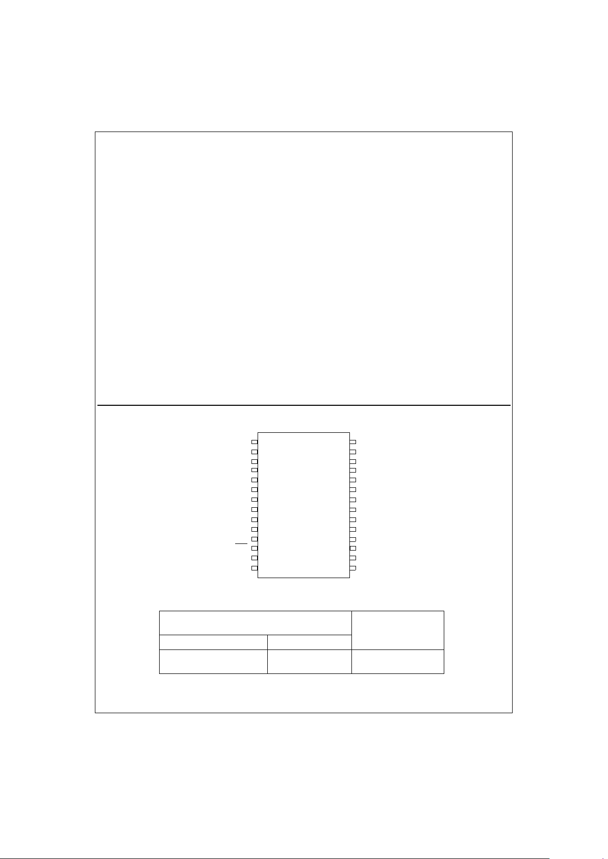
LM9822 3 Channel 42-Bit Color Scanner Analog Front End
Connection Diagram
LM9822
28 pin
SOIC
SCLK
SDI
SEN
D2
D0
V
D
DGND
D4
11
12
13
14
15
16
17
18
19
20
1
2
3
4
5
6
7
8
9
10
23
22
21
24
25
26
27
28
D7
D6
D5
MCLK
V
A
V
A
V
REF-
OS
B
OS
G
CLMP
OS
R
V
REF+
AGND
AGND
VSMP
SDO
V
REFMID
V
BANDGAP
D3
D1
May 1999
LM9822 3 Channel 42-Bit Color Scanner Analog Front End
N
©1999 National Semiconductor Corporation
TRI-STATE® is a registered trademark of National Semiconductor Corporation.
Ordering Information
Notes: 1 - Rail tran spo r t med i a, 2 6 pa rt s per rail, 2 - Tape and reel transport media, 1000 parts per reel
Temperature Range
0°C ≤ T
A
≤ +70°C
NS Package
Number
Order Number Device Marking
LM9822CCWM
1
LM9822CCWMX
2
LM9822CCWM
LM9822CCWM
M28B
M28B
Page 2
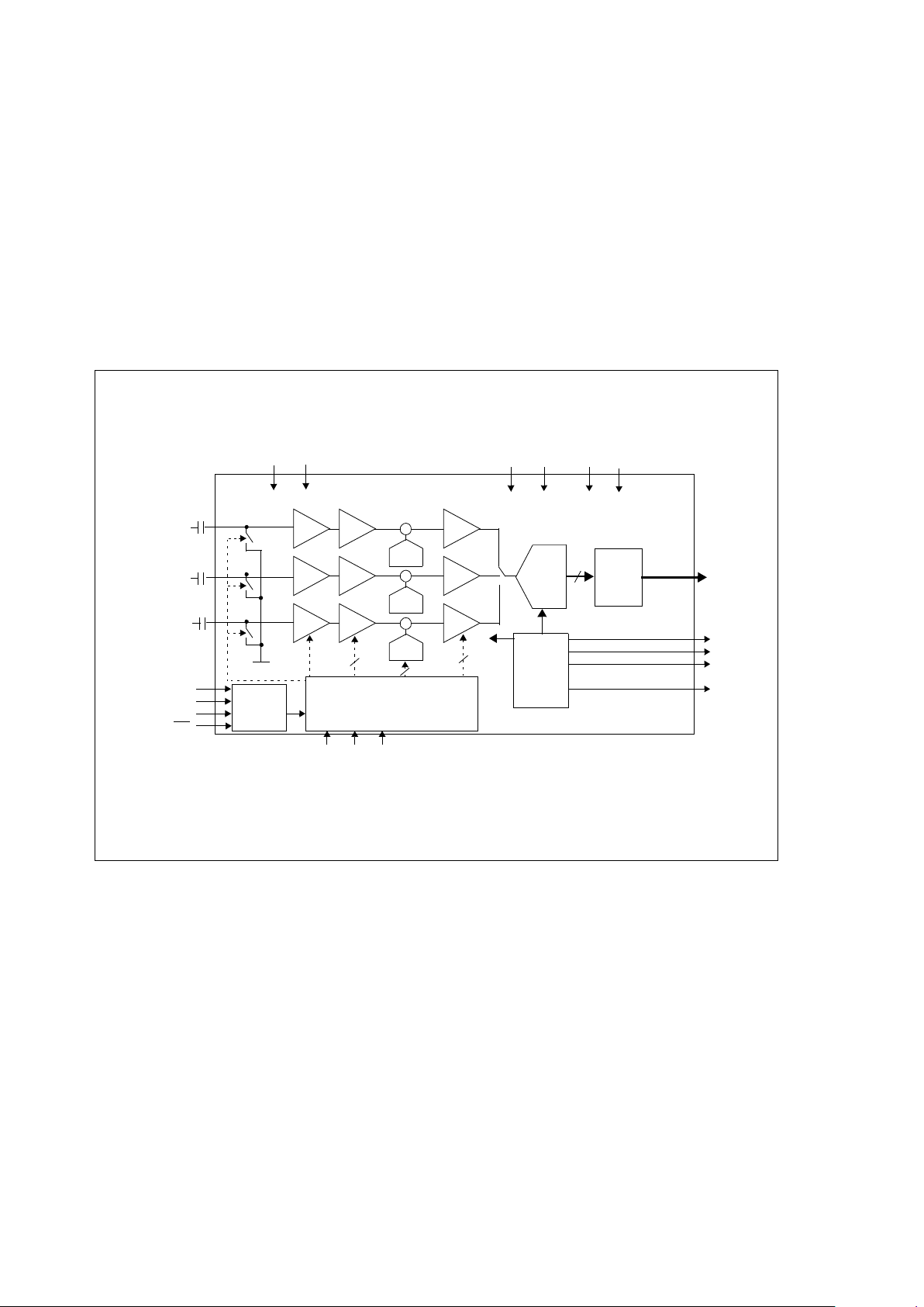
LM9822 Block Diagram
Serial
Interface
Coarse Color
Balance PGAs
DAC
R
Offset
+
+
OS
R
RED OS
from CCD
CDS
OS
G
GREEN OS
from CCD
CDS
OS
B
BLUE OS
from CCD
CDS
x0.93
to x3
DAC
G
Offset
+
+
DAC
B
Offset
+
+
VClamp
x1or x3
Static
Offset
DACs
V
BANDGAP
V
REF+
V
REFMID
V
REF-
Internal
Bandgap
Reference
x1or x3
x1or x3
Gain
Boost
x0.93
to x3
x0.93
to x3
Timing and Control
14
5
6
1
SCLK
SDI
SEN
V
A
V
D
AGND
DGNDVAAGND
MCLK
14 bits
to 8 bit
Bytes
D7 - D0
CLMP VSMP
14-Bit
ADC
SDO
2 www.national.com
Page 3
3 www.national.com
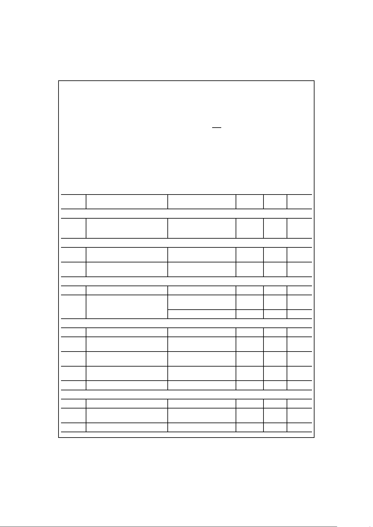
Electrical Characteristics
The following specifications apply for AGND=DGND=0V, VA=+5.0V
DC
,
V
D
=+3.0 or +5.0VDC, f
MCLK
=12MHz.
Boldface limits apply
for T
A=TJ=TMIN
to T
MAX
; all other limits TA=TJ=25°C. (Notes 7, 8, 12 & 16)
Symbol Parameter Conditions
Typical
(Note 9)
Limits
(Note 10)
Units
(Limits)
CCD/CIS Source Requirements for Full Specified Accuracy an d Dynamic Range
(Note 12)
V
OS PEAK
Sensor’s Maximum Peak Differential
Signal Range
Gain = 0.933
Gain = 3.0
Gain = 9.0
2.1
0.65
0.21
V
V
V
Full Channel Linearity (In un it s of 12 bit LSBs)
(Note 14)
DNL Differential Non-Linearity
+0.9
-0.4
+2
-0.9
LSB(max)
INL Integral Non-Linearity Error (Note 11) ±2.2
+5
-7
LSB(max)
Analog Input Characteristics
OS
R
,
OS
G
,
OS
B
Input Capacitance 5 pF
OS
R
,
OS
G
,
OS
B
Input Leakage Current
Measured with OS = 3.5V
DC
CDS disabled
20
25
µA (max)
CDS enabled 10 nA
Coarse Color Balance PGA Characteristics
Monotonicity
5
bits (min)
G
0
(Minimum PGA Ga in) PGA Setting = 0 0.93
.90
.96
V/V (min)
V/V (m ax)
G
31
(Maximum PGA Gain) PGA Setting = 31 3.0
2.95
3.07
V/V (min)
V/V (m ax)
x3 Boost Gain
x3 Boost Setting On
(Bit 5 of Gain Register is set)
3.0
2.86
3.08
V/V (min)
V/V (m ax)
Gain Error at any gain (Note 13) ±0.3
1.6
% (max)
Static Offset DAC Characteristics (In units of 12 bit LSBs)
Monotonicity
6
bits (min)
Offset DAC LSB size PGA gain = 1 18.9
13
24
LSB (min)
LSB (max)
Offset DAC Adjustment Range PGA gain = 1 ±585
±570
LSB (min)
Positive Supply Voltage (V+=VA=VD)
With Respect to
GND=AGND=DGND
6.5V
Voltage On Any Input or Output Pin -0.3V to V
+
+0.3V
Input Current at any pin (Note 3) ±25mA
Package Input Current (Note 3) ±50mA
Package Dissipation at T
A
= 25°C (Note 4)
ESD Susceptibility (Note 5)
Human Body Model 7000V
Machine Model 450V
Soldering Information
Infrared, 10 seconds (Note 6) 235°C
Storage Temperature -65°C to +150°C
Operating Temperature Range T
MIN
=0°C≤TA≤T
MAX
=+70°C
V
A
Supply Voltage +4.75V to +5.25V
V
D
Supp l y Voltage +3.0V to +5.25V
V
D-VA
≤ 100mV
OS
R
, OSG, OS
B
Input Voltage Range -0.05V to A + 0.05V
SCLK, SDI, SEN
, MCLK, VSMP, CLMP
Input Voltage Range -0.05V to V
D
+ 0.05V
Absolute Maximum Ratings
(Notes 1& 2)
Operating Ratings
(Notes 1& 2)
Page 4
4 www.national.com
Symbol Parameter Conditions
Typical
(Note 9)
Limits
(Note 10)
Units
(Limits)
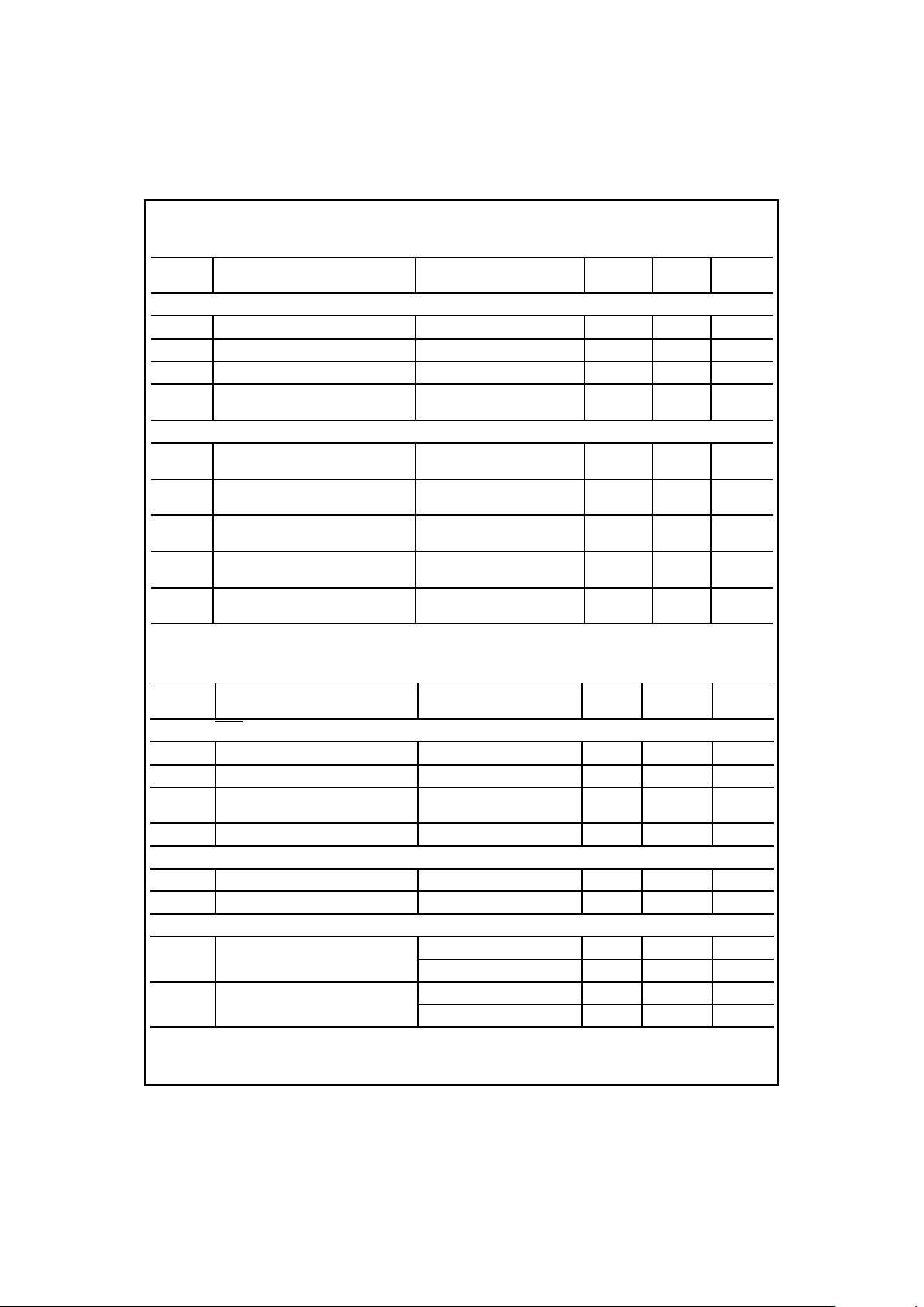
Internal Reference Characteristics
V
REFMID
Mid Reference Output Voltage 2.5 V
V
REF+ OUT
Positive Reference Output Voltage 3.5 V
V
REF- OUT
Negative Reference Output Voltage 1.5 V
∆V
REF
Differential Reference Voltage
V
REF+ OUT
- V
REF- OUT
2.0 V
System Characteristics (In units of 12 bit LSBs) (see section 5.1, Internal Offsets)
C
Analog Channel Gain Constant
(ADC Codes/V)
Includes voltage reference
variation, gain setting = 1
2107
1934
2281
LSB (min)
LSB (max)
V
OS1
Pre-Boost Analog Channel Offset Error,
CCD Mode
17.3
-61
+94
LSB (min)
LSB (max)
V
OS1
Pre-Boost Analog Channel Offset Error,
CIS Mode
27
-49
+103
LSB (min)
LSB (max)
V
OS2
Pre-PGA Analog Channel Offset Error -40
-124
+44
LSB (min)
LSB (max)
V
OS3
Post-PGA Analog Channel Offset Error -38
-130
+55
LSB (min)
LSB (max)
DC and Logic Electrical Characteristics
The following specifications apply for AGND=DGND=0V, VA=+5.0V
DC
,
V
D
=+3.0 or +5.0VDC, f
MCLK
=12MHz.
Boldface limits apply
for T
A=TJ=TMIN
to T
MAX
; all other limits A=TJ=25°C. (Notes 7& 8)
Symbol Parameter Conditions
Typical
(Note 9)
Limits
(Note 10)
Units
(Limits)
SCLK, SDI, SEN,
MCLK, VSMP, CLMP Digital Input Characteristics
V
IN(1)
Logical “1” Input Voltage VA=5.25V
2.0
V (max)
V
IN(0)
Logical “0” Input Voltage VA=4.75V
0.8
V (min)
I
IN
Input Leakage Current
V
IN
=V
A
VIN=DGND
0.1
-0.1
µA(max)
µA(max)
C
IN
Input Capacitance 5 pF
D0-D7 Digital Output Characteristics
V
OUT(1)
Logical “1” Output Voltage I
OUT
=-360µA
0.8*V
D
V (min)
V
OUT(0)
Logical “0” Output Voltage I
OUT
=1.6mA
0.2*V
D
V (max)
Power Supply Characteristics
I
A
Analog Supply Current
Operating 75
108
mA (max)
Power Down 675
900
µA (max)
I
D
Digital Supply Current (Note 15)
Operating 210
475
µA (max)
Power Down 2
25
µA (max)
Electrical Characteristics
(Continued)
The following specifications apply for AGND=DGND=0V, V
A
=+5.0V
DC
,
V
D
=+3.0 or +5.0VDC, f
MCLK
=12MHz.
Boldface limits apply
for T
A=TJ=TMIN
to T
MAX
; all other limits TA=TJ=25°C. (Notes 7, 8, 12 & 16)
Page 5
5 www.national.com
AC Electrical Characteristics
The following specifications apply for AGND=DGND=0V, VA=+5.0V
DC
,
V
D
=+3.0 or +5.0VDC, f
MCLK
=12MHz, except where noted
otherwise.
Boldface li mit s apply for
A=TJ=TMIN
to T
MAX
; all other limits TA=TJ=25°C. (Notes 7& 8)
Note 1:
Absolute Maximum Ratings indicate limits beyond which damage to the device may occur. Operating Ratings indicate conditions for which the device is functional,
but do not guarantee specific performance limits. For guaranteed specifications and test conditions, see the Electrical Characte ristics. The guaranteed specifications apply
only for the test conditions listed. Some performance characteristics may degrade when the device is not operated under the list ed te st con di tions.
Note 2:
All voltages are measured with respect to GND=AGND=DGND=0V, unless otherwise specified.
Note 3:
When the input voltage (V
IN
) at any pin exceeds the power supplies (VIN<GND or VIN>VA or
V
D
), the current at that pin should be limited to 25mA. The 50m
maximum pac kage input c urre nt ra tin g limits the nu mb er of pin s that can simultaneously safely exceed the power supplies with an input current of 25mA to two.
Note 4:
The maximum power dissipation must be derated at elevated temperatures and is dictated by T
J
max,
Θ
JA
and the ambient temperature, TA. Th e maximum allow-
able power dissipation at any temperature is P
D
= (TJmax - TA) /
Θ
JA
. TJmax = 150°C for this device. The typ ica l t he rmal resi stance (
Θ
JA
) of this p a rt when board mounted
is 69°C /W for the M28 B SOIC package
.
Note 5:
Human body model, 100pF capacitor discharged through a 1.5kΩ resistor. Machine model, 200 pF capacitor discharged through a 0Ω resistor.
Note 6:
See AN450 “Surface Mounting Methods and Their Effect on Product Reliability” or the section titled “Surface Mount” found in any National S e miconductor Linear
Data Book for other methods of so l de r i ng sur f a ce m ount devices.
Note 7:
Two diodes clamp the OS analog inputs to
AGND
and
V
A
as shown below. This input protection, in combination with the external clamp capacitor and the output
impedance of the sensor, prevents damage to the LM9822 from transients during power-up.
Note 8:
To guarantee accuracy, it is required that V
A
and VD be connected to clean, low noise power supplies, with separate bypass capacitors at each supply pin. When
both V
A
and VD are operated at 5.0V, they must be powered by the same regulator, with separate power planes or traces and separate bypass capaci to rs at each suppl y pin.
Sym b ol Paramete r Condi tions
Typi cal
(Note 9)
Limits
(Note 10)
Units
(Limits)
f
MCLK
Maximum MCLK frequency
12
MHz (min)
t
MCLK
MCLK period 83 ns (min)
MCLK duty cycle
40
60
%(min)
%(max)
t
SCLK
Serial Clock Period
1
t
MCLK
(min)
t
SEN
Serial Enable high time
3
t
MCLK
(min)
t
SSU
SDI setup time
1
ns (min)
t
SH
SDI hold time
3
ns (min)
t
SDDO
SCLK
edge to new valid data
V
D
= 5.0V
V
D
= 3.3V
8.5
19
20
ns (max)
t
VSU
VSMP setup time
1
ns (min)
t
VH
VSMP hold time
3
ns (min)
t
CSU
CLMP setup time
1
ns (min)
t
CH
CLMP hold time
3
ns (min)
t
DDO
MCLK
edge to new valid data
V
D
= 5.0V
V
D
= 3.3V
16
25
25
ns (max)
ns (max)
OS Input
AGND
V
A
TO INTERN AL
CIRCUITRY
Page 6
6 www.national.com
Electrical Characteristics
(Continued)
Note 9:
Typicals are at T
J=TA
=25°C, f
MCLK
= 12MHz, and represent most likely parametric norm.
Note 10:
Tested limits are guaranteed to National's AOQL (Average O utgoing Quality Level).
Note 11:
Full channe l integral non-linea rity error is defined a s the d eviation of the analog v alue , expres sed in LSB s, from the straight line tha t best fits th e a ct u al transfer
function of th e AFE.
Note 12:
The sensor’s maximum peak differential signal range is defined as the peak sensor output voltage for a white (full scale) image, with respect to the dark reference
level.
Note 13:
PGA Gain Error is the maximum difference between the measured gain for any PGA code and the ideal gain calculated using:
where .
Note 14:
Full Channel IN L and DN L are te st e d w i th C DS disab le d, negative sign al pola rity , DOE = 0, and a si ngle OS inpu t with a gain register se ttin g of 1 (0 00 0 0 1b) and
an offset re gi st er s et ti ng o f 0 (0 00 000b).
Note 15:
The digital supply current (ID) does not include the load, data and switching frequency dependent current required to drive the digital output bus on pins (D7 - D0).
The curre nt requir ed to switch t he digita l d ata bus can be calc ulate d f rom : Isw = 2*N d*Psw* CL*V
D/tMCLK
where N d is total num ber of da ta pins, Psw is the pr obability of
each data bit switching, CL is the capacitive loading on each d ata pin, V
D
is the digital supply voltage and t
MCLK
is the period of the MCLK input. For most applications, Nd
is 8, Psw is ≈ 0.5, and V
D
is 5V, and the switching current can be calculated from: Isw = 40*CL/tMCLK. (With D at 3.3V, the equation bec omes : Isw = 2 6.4*CL/t
MCLK
.) For
example, if the capacitive load on each digital output pin (D7 - D0) is 20pF and the period of t
MCLK
is 1/12MHz or 83ns, then the digital switching current would be 9.6mA.
The calculated digital switching current will be drawn through the V
D
pin and should be c on s idere d a s part of th e total po wer bu d ge t for the LM9822.
Note 16:
All specifications quoted in LSBs are based on 12 bit resolution.
V
WHITE
V
REF
V
RFT
CCD Output Signal
CIS Output Signal
V
WHIT
Black Level
Gain
PGA
V
V
--- -
G0X
PGA code
32
-------------- -------------- -+=XG
31G0
–
()
32
31
----- -=
Page 7
7 www.national.com
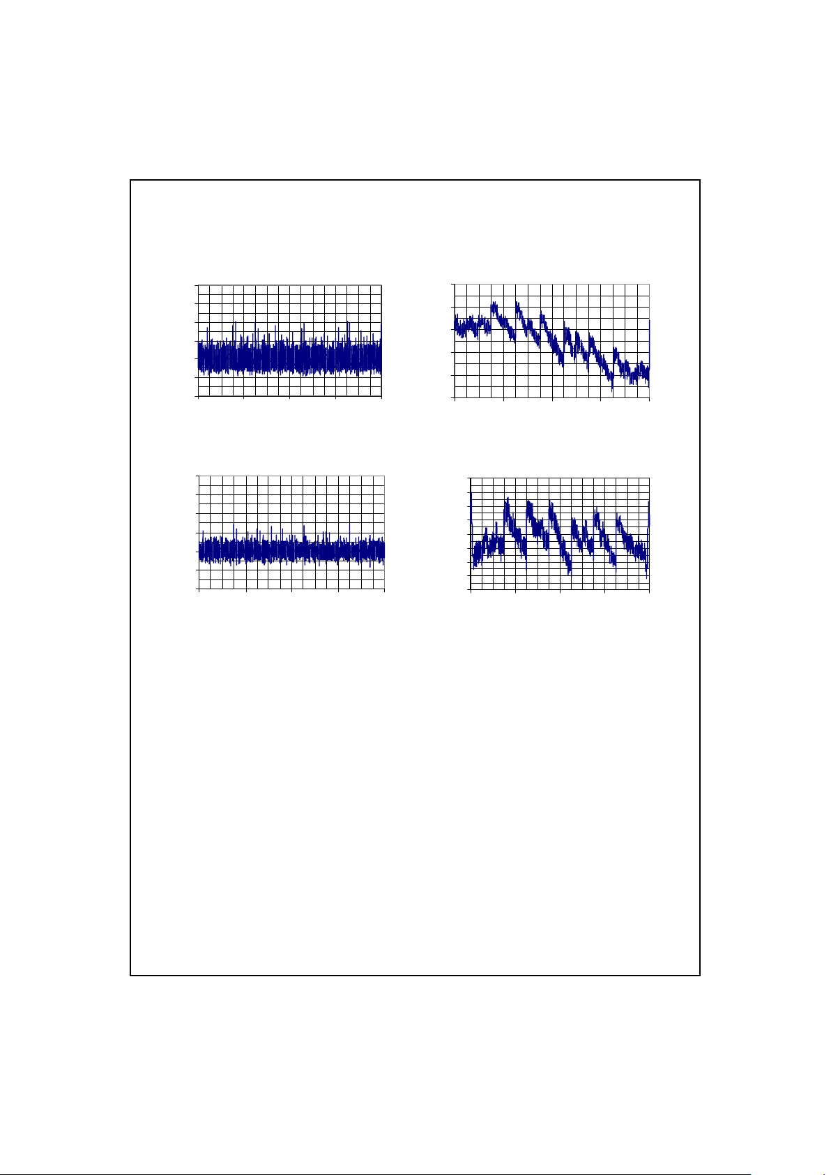
Typical Performance Characteristics
Full Channel DNL and INL
(Divide by 2, Monochrome Mode, 6 MHz Pixel Rate)
Note:
The LM9822 provides 14-bit data for high resolution imaging applications. The typical full channel device performance is shown
in the above graphs. In many applications, particularly those where high speed is important, or where lower cost CCD and CIS sensors
are used, the signal source is only accurate to 12 bits. In these applications, only 12-bit of data may be used. 12-bit DNL and INL pl ots
have also been provided to illustrate the performance of the LM9822 in these applications.
Typical 12 Bit DNL
-1
-0.5
0
0.5
1
1.5
2
0 1024 2048 3072 4096
Output Code
LSB
Typical 12 Bit INL
-2.5
-2
-1.5
-1
-0.5
0
0.5
1
1.5
0 1024 2048 3072 4096
Output Code
LSB
Typical 14 Bit DNL
-1
-0.5
0
0.5
1
1.5
2
0 4096 8192 12288 16384
Output Code
LSB
Typical 14 Bit INL
-15
-10
-5
0
5
10
0 4096 8192 12288 16384
Output Code
LSB
Page 8

8 www.national.com
Pin Descriptions
Connection Diagram
Analog Power
V
A
The two A pins are the analog supply pins.
They should be connected to a voltage
source of +5V and bypassed to
AGND
with a
0.1µF monolithic capacitor in parallel with a
10µF tantalum capacitor.
AGND
These two pins are the ground returns for
the analog supplies.
V
D
This is the positive supply pin for the digital
I/O pins. It should be connected to a voltage
source between +3.3V and +5.0V and be
bypassed to DGND with a 0.1µF monolithic
capacitor in parallel with a 10µF tantalum
capacitor.
DGND
This is the ground return for the digital supply.
Analog In put /O utpu t
OS
R
,
OS
G
,
OS
B
Analog Inputs. These inputs (for Red,
Green, and Blue) should be tied to the sensor’s OS (Output Signal) through DC blocking capacitors.
V
REF+
,
V
REFMID
,
V
REF-
Voltage reference bypass pins. V
REF+
,
V
REFMID
, and V
REF-
should each be
bypassed to
AGND
through a 0.1uF mono-
lithic ca pacitor.
Timing Control
MCLK
Master clock input. The ADC conversion
rate will be 1/2 of MCLK. 12MHz is the maximum frequency for MCLK.
VSMP
Sample timing input signal. If VSMP is high
on the rising edge of MCLK, the input is
sampled on the rising edge of the next
MCLK. The reference signal for the next
pixel will be sampled one to four MCLKs
later, depending on the value in the
CDSREF configuration bits. If CDS is not
enabled, the internal reference will be sampled during the reference sample time.
The number of MCLK cycles between
VSMP pulses determines the pixel rate.
Timing Diagrams 1 through 6 illustrate the
VSMP timings for all the valid pixel rates.
Note: See the applications section of the
datasheet for the proper timing relationships
between VSMP and MCLK.
CLMP
Clamp timing input. If CLMP and VSMP are
high on the ri sing edge of MCLK, all three
OS inputs will be internally connected to
V
CLAMP
during the next pixel.
V
CLAMP
is either
VREF+ or VREF- depending on the state of
the Signal Polarity bit in the Sample Mode
register (Reg. 0, Bit 4).
Data Output
D7-D0
Data Output pins. The 14 bit conversion
results of the ADC are multiplexed in 8 bit
bytes to
D7-D0
synchronous with MCLK.
The MSB consists of data bits d13-d6 on
pins D7-D0 and the LSB consists of d5-d0
on pins D7-D3 with D1 and D0 low.
Serial Input/Output
SCLK
Serial Shift Clock. Input data on SDI is valid
on the rising edge of SCLK. The minimum
SCLK period is 1 t
MCLK
.
SDO
Serial Data Output. Data bits are shifted out
of SDO on falling edges of SCLK. The first
eight falling edges of SCLK after SEN goes
low will shift out eight data bits (MSB first)
from the configuration register addressed
during the previous SEN
low time.
SDI
Serial Data Input. A read/write bit, followed
by a four address bits and eight data bits is
shifted into SDI, MSB first. Data should be
valid on the rising edge of SCLK. If the
read/write bit is a “0” (a write), then the
shifted data bits will be stored. If the
read/write bit is a “1” (a read), then the data
bits will be ignored , and SDO will shift out
the addressed register’s contents during the
next SEN
low time.
SEN
Shift enable and load signal. When SEN is
low, data is shifted into SDI. When SEN
goes high, the last thirteen bits (one
read/write, four address and eight data)
shifted into SDI will be used to program the
addressed configuration register. SEN
must
be high for at least 3 MCLK cycles between
SEN
low times.
LM9822
28 pin
SOIC
SCLK
SDI
SEN
D2
D0
V
D
DGND
D4
11
12
13
14
15
16
17
18
19
20
1
2
3
4
5
6
7
8
9
10
23
22
21
24
25
26
27
28
D7
D6
D5
MCLK
V
A
V
A
V
REF-
OS
B
OS
G
CLMP
OS
R
V
REF+
AGND
AGND
VSMP
SDO
V
REFMID
V
BANDGAP
D3
D1
Page 9

9 www.national.com
Timing Diagrams
OSR,
Diagram 1:
Divide by 6 Color Mode Sample and Data Output Timing
VSMP
OSG,
OS
B
D7 -D0
Sample Signal
Sample Reference
MCLK
Level
Level
GH GL BLBH RH RL GH GL BH BL
H = d13-d6
L = d5-d0
ADC Clock
(internal)
N+1N
N
N-1
RH
N-4N-5N-5 N-4 N-4
DOE (Register 0, Bit 4) = 0
Diagram 2:
Divide by 6 Monochrome Mode Sample and Data Output Timing (Green Input shown)
VSMP
OS
G
D7 -D0
Sample Signal
Sample Reference
MCLK
Level
Level
XX XX XXXX GH GL XX XX XX XX
H = d13-d6
L = d5-d0
ADC Clock
(internal)
NN-1
N+1
N
GH
N-4
DOE (Register 0, Bit 4) = 0
OSR,
Diagram 3:
Divide by 8 Color Mode Sample and Data Output Timing
VSMP
OSG,
OS
B
D7 -D0
Sample Signal
Sample Reference
MCLK
Level
Level
RH RL GLGH BH BL XX XX RH RLXX
H = d13-d6
L = d5-d0
ADC Clock
(internal)
N-1
N
N
N+1
GH
N-4 N-4 N-4
N-3
DOE (Register 0, Bit 4) = 0
Page 10

10 www.national.com
Timing Diagrams
(Continued)
Diagram 4:
Divide by 8 Monochrome Mode Sample and Data Output T im in g (Gre en Input Shown)
VSMP
OS
G
D7 -D0
Sample Signal
Sample Reference
MCLK
Level
Level
GH GL XXXX XX XX XX XX GH GLXX
H = d13-d6
L = d5-d0
ADC Clock
(internal)
N-1
N
N
N+1
N-4 N-3
XX XX
DOE (Register 0, Bit 4) = 0
Diagram 5:
Divide by 3 Monochrome Mode Sample and Data Output Timing (Green Input shown)
VSMP
D7 -D0
Sample Signal
Sample Reference
MCLK
Level
Level
GH GL GH GL GH GL GH
H = d13-d6
L = d5-d0
ADC Clock
(internal)
OS
G
CDSREF = 00
N
N
N-1
N+1
N+1
N+2
N+2
N-11 N-10 N-9
GL
DOE (Register 0, Bit 4) = 0
Diagram 6:
Divide by 2 Monochrome Mode Sample and Data Output Timing (Green Input shown)
VSMP
D7 -D0
Sample Signal
Sample Reference
MCLK
Level
Level
GH GL GLGH GH GL GH GL GH GL
H = d13-d6
L = d5-d0
ADC Clock
(internal)
OS
G
CDSREF = 00
N
N
N+1
N+1
N+2
N+2
N+3
N+3N-1
N-1
N+4
N-11 N-10 N-9 N-8 N-7
DOE (Register 0, Bit 4) = 0
Page 11

11 www.national.com
Timing Diagrams
(Continued)
Diagram 7:
Programmable Reference Sample Timing
VSMP
D3 -D0
Sample Signal
Sample Reference
MCLK
OSR,OSG,
OS
B
CDSREF=00 CDSREF=01 CDSREF=10 CDSREF=11
Diagram 8:
Clamp Timing With SMPCL = 0
VSMP
Sample Signal
Sample Reference
MCLK
OS
CDSREF = 00
N
N
N-1
N+1
N+1
N+2
N+2
CLMP
Clamp On
(internal signal)
Diagram 9:
Clamp Timing With SMPCL = 1
VSMP
Sample Signal
Sample Reference
MCLK
OS
CDSREF = 00
N
N
N-1
N+1
N+1
N+2
N+2
CLMP
Clamp On
(internal signal)
Diagram 10:
Configuration Register Serial Write Timing
SEN
SDI
SCLK
0 A3 A2 A1 A0 D7 D6 D5 D4 D3 D2 D1 D0 XXXX
R/W bit
Diagram 11:
Configuration Register Serial Read Timing
SEN
SDI
SCLK
1
A3 - A0
XX XX
SDO
XX
b7 - b0
1
A3 - A0
R/W bit
Page 12

12 www.national.com
Timing Diagrams
(Continued)
Diagram 12:
Serial Input and Output Timing
SEN
SDI
SCLK
D0
SDO
D1D2
D5D6D7
A2A3R/W D7A1 A0XX
XX D2D3D4
t
SDDO
t
SH
t
SSU
t
SH
t
SSU
t
SEN
t
SCLK
1/2 t
SCLK
1/2 t
SCLK
Diagram 13:
MCLK, VSMP and CLMP Input Timing and Data Output Timing
VSMP
MCLK
D7 - D0
DOE = 0
CLMP
t
VSUtVH
t
CH
t
CSU
t
MCLK
t
DDO
D7 - D0
DOE = 1
t
DDO
Page 13

13 www.national.com
Table 1: Configuration Register Address Table
Address
(Binary)
Register Name and Bit Definitions
A3 A2 A1 A0 B7 B6 B5 B4 B3 B2 B1 B0
0000
Sample Mode (Power Up Default = 62h)
I/O Mode DOE CDS Polarity SMPCL CDSREF1 CDSREF0 PD
0001
Red Offset Setting (Power Up Default = 00h)
N/A N/A
Polarity MSB LSB
0010
Green Offset Setting (Power Up Default = 00h)
N/A N/A
Polarity MSB LSB
0011
Blue Offset Setting (Power Up Default = 00h)
N/A N/A
Polarity MSB LSB
0100
Red Gain Setting (Power Up Default = 00h)
N/A N/A
x3 MSB LSB
0101
Green Gain Setting (Power Up Default = 00h)
N/A N/A
x3 MSB LSB
0110
Blue Gai n Set ting (Powe r Up D efaul t = 0 0 h )
N/A N/A
x3 MSB LSB
0111
Color Mode (Power Up Default = 00h)
N/A N/A N/A N/A N/A N/A
CM1 CM0
1000
Test Register 0 (Power Up Default = 00h)
00000000
1001
Test Register 1 (Power Up Default = 10h)
00010000
1010
Test Register 2 (Power Up Default = 00h)
00000000
Page 14

14 www.national.com
Table 2: Configuration Register Parameters
Power-Up Default Register Settings are shown in
Bold Italic s
Parameter
(Address)
Control Bits Result
Sample Mode (0)
I/O Mode
(0)
B7
0
1
Normal Output Driver Operation
Reduced Slew Rate Output Driver Operation
DOE
(Data Output Edge)
(0)
B6
0
1
D7-D0 are clocked out (change) on the falling edge of MCLK - Recommended setting for
lowest noise and best overall performance.
D7-D0 are clocked out (change) on the rising edge of MCLK
CDS (Enable)
(0)
B5
0
1
CDS disabled (CIS)
CDS Enabled (CCD)
Signal Pol arit y
(0)
B4
0
1
Negative Polarity (CCD) Clamping to V
REF+
Positive Polarity (CIS) Clamping to V
REF-
SMPCL
(0)
B3
0
1
Clamp is on for 1 MCLK before reference sampled
Clamp is on between the reference and the signal sample points
CDSREF
(0)
B2
0
0
1
1
B1
0
1
0
1
Reference (for pixel N+1) sampled 1 MCLK cycle after signal (for pixel N) sampled
Reference (for pixel N+1) sampled 2 MCLK cycle after signal (for pixel N) sampled
Reference (for pixel N+1) sampled 3 MCLK cycle after signal (for pixel N) sampled
Reference (for pixel N+1) sampled 4 MCLK cycle after signal (for pixel N) sampled
PD
(Powe r Down)
(0)
B0
0
1
Operating
Low Power Standby
Page 15

15 www.national.com
Red, Green and Blue Offset DAC Settings ( 1, 2 & 3)
Offset Polarity
B5
0
1
Positive Offset
Negative Offset
Offset Value
B4(M
SB)
B3 B2 B1 B0(LSB) Typical Offset = 20LSBs * Offset Value * PGA Gain
Typical Offset
Values
B5
(SIGN
)
0
0
0
• • •
0
0
1
1
1
• • •
1
1
B4
(MSB)
0
0
0
• • •
1
1
0
0
0
• • •
1
1
B3
0
0
0
• • •
1
1
0
0
0
• • •
1
1
B2
0
0
0
• • •
1
1
0
0
0
• • •
1
1
B1
0
0
1
• • •
1
1
0
0
1
• • •
1
1
B0
(LSB)
0
1
0
• • •
0
1
0
1
0
• • •
0
1
Typical Offset (with PGA Gain = 1)
12 bit LSBs
0.00
+20
+40
• • •
+600
+620
0
-20
-40
• • •
-600
-620
Red, Green and Blue Gain Settings (4, 5 & 6)
Boost Gain Enable
B5
0
1
Boost Gain = 1V/V
Boost Gain = 3V/V
PGA Gain Value
B4(M
SB)
B3
B2 B1 B0(LSB)
PGA Gain (V/V) =.933 + 0.0667 * (PGA Gain Value)
Gain
Gain = Boost Gain * PGA Gain
Table 2: Configuration Register Parameters
(Continued)
Power-Up Default Register Settings are shown in
Bold Italics
Parameter
(Address)
Control Bits Result
Page 16

16 www.national.com
Typical Gain Values
B5
(
x3)
0
0
0
• • •
0
0
0
• • •
1
1
1
• • •
1
1
1
B4
(MSB)
0
0
0
• • •
1
1
1
• • •
0
0
0
• • •
1
1
1
B3
0
0
0
• • •
1
1
1
• • •
0
0
0
• • •
1
1
1
B2
0
0
0
• • •
1
1
1
• • •
0
0
0
• • •
1
1
1
B1
0
0
1
• • •
0
1
1
• • •
0
0
1
• • •
0
1
1
B0
(LSB)
0
1
0
• • •
1
0
1
• • •
0
1
0
• • •
1
0
1
Typical Gain
(V/V)
0.93
1.00
1.07
• • •
2.87
2.93
3.00
• • •
2.79
3.00
3.20
• • •
8.60
8.80
9.00
Color Mode (7)
Color Mode
B1
0
0
1
1
B0
0
1
0
1
Color
Monochrome - Red
Monochrome - Green
Monochrome - Blue
Reserved Register 0 (8)
Reserved
Register 0
0 0 0 0 0 0 0 0
Reserved, always set to 00h.
Reserved Register 1 (9)
Reserved
Register 1
0 0 0 1 0 0 0 0
Reserved, always set to 10h.
Reserved Register 2 (A)
Reserved
Register 2
0 0 0 0 0 0 0 0
Reserved, always set to 00h.
Table 2: Configuration Register Parameters
(Continued)
Power-Up Default Register Settings are shown in
Bold Italics
Parameter
(Address)
Control Bits Result
Page 17

17 www.national.com
Applications Information
1.0 Introduction
The LM982 2 is a high performance scanner Analog Font End
(AFE) for image sensor processing systems. It is designed to
work with color CCD and CIS image sensors and provides a full 3
channel sampling, gain and offset correction system, coupled
with a 14 bit high speed analog to digital converter. A typical
application of the LM9822 is in a color flatbed document scanner.
The image sensing and processing portion of the system would
be configured similar to that shown in Figure 1.
Figure 1: LM9822 in Basic Color Scanner
2.0 CDS Correlated Double Sampler
The LM9822 uses a high-performance CDS (Correlated Double
Sampling) circuit to remove many sources of noise and error from
the image sensor output signal. It also supports CIS image sensors with a single ended sampling mode.
Figure 2 shows the output stage of a typical CCD and the resulting output waveform:
Figure 2: CDS
Capacitor C1 converts the electrons coming from the CCD’s shift
register to an analog voltage. The source follower output stage
(Q2) buffers this volta ge before it leaves the CCD. Q1 resets the
voltage across capacitor C1 between pixels at intervals 2 and 5.
When Q1 is on, the output signal (OS) is at its most positive voltage. After Q1 tu rns off (period 3), the OS level repre sents the
residual voltage across C1 (V
RESIDUAL
). V
RESIDUAL
includes
charge injection from Q1, therma l noise from the ON resistance
of Q1, and other sources of error. When the shift register clock
(Ø1) makes a low to high transition (period 4), the electrons from
the next pi xel flow into C 1. The ch arge across C1 now contains
the voltage proportional to the number of electrons plus V
RESID-
UAL
, an error term. If OS is sampled at the end of period 3 and
that voltage is subtracted from the OS at the end of period 4, the
V
RESIDUAL
term is canceled and the noise on the signal is
reduced ([V
SIGNAL+VRESIDUAL
]-V
RESIDUAL
= V
SIGNAL
). This is the
principal of Correlated Double Sampling.
3.0 CIS Mode (CDS Off, Selectable Signal Polarity)
The also LM9822 supports CIS (Contact Image Sensor) devices.
The output sig nal of a CIS sensor (Figure 3) differs from a CCD
signal in two primary ways: its output usually increases with
increasing signal strength, and it does not usually have a reference level as an integral part of th e output waveform of every
pixel.
Figure 3:
CIS
When the LM9822 is in CIS (CDS off) mode (Register 0, B5=1), it
uses either
V
REF+
or
V
REF-
as the reference (or black) voltage for
each pixel (depending on th e signal polarity setting (Register 0,
Bit 4)). If the s ignal polarity i s set to one, then
V
REF-
will be sam-
pled as the reference level. If it is set to zero, then
V
REF+
will be
sampled as the reference level.
4.0 Programmable Gain
The output of the Sampler drives the input of the x3 Boost gain
stage. The gain of each x3 Boost gain is 3V/V if bit B5 of that
color’s gain register (register 4,5, or 6) is set, or 1V/V if bit B5 is
cleared. The output of eac h x3 gain stage is the input an offset
DAC and the output of each offset DAC is the input to a PGA
(Programmable Gain Amplifier). Each PGA provides 5 bits of gain
correction over a 0.93V/V to 3V/V (-0.6 t o 9.5dB) range. The x3
Boost gain stage and t he PGA can be combined for an overall
gain range of 0.93V/V to 9.0V/V (-.6 to 19dB). The gain setting for
each color (registe rs 4, 5 and 6) shou ld b e s et during calibration
to bring th e maximum amplitude of the stron gest pixel to a level
just below the desired maximum output from the ADC. The PGA
gain is determined by the following equation:
If the x3 Boost gain is enabled then the overall s ignal gain will be
three times the PGA gain.
ASIC
LM9822
CCD
RAM
8 Output Data
8
OS
R
OS
G
OS
B
CCD Control
AFE Control
To H ost
Other scanner elements
omitted for simplicity.
RS (RESET)
e-
(from shift register)
OS
Q1
Q2
C1
V
DD
V
SS
Ø1
RS
OS
123 4 5
OS (CCD)
123 4 5
OS (CIS)
PGA Gain
V
V
--- -
0.933 + .0667 (value in bits B4-B0)=
Equation 1:
PGA Gain
Page 18

18 www.national.com
5.0 Offset DAC
The Offset DACs remove the DC offsets generated by the sensor
and the LM9822’s analog signal chain (see section 5.1, Inter nal
Offsets). The DAC value for each color (registers 1,2 and 3)
should be set during calibration to the lowest value that still
results in an ADC output code greater than zero for all the pixels
when scanning a black line. With a PGA gain of 1V/V, each LSB
of the offset DAC typically adds the equivalent of 20 ADC LSBs,
providing a total offset adjustment range of ±590 ADC LSBs. The
Offset DAC’s output voltage is given by:
In terms of 12 bit output codes, the offset is given by:
The offset is positive if bit B5 is cleared and negative if B5 is set.
Since the anal og of fset is added before the PGA gain, the value
of the PGA gain m ust be cons idered when selecting the offset
DAC values.
5.1 Internal Offsets
Figure 4 is a mod el o f the LM9822’s internal off sets. Equation 4
shows how to calculate the expected output code given the input
voltage (V
IN
), the L M98 22 in te rna l o ffsets (
OS1
, V
OS2
, V
OS3
),
the programmed offset DAC voltage (V
DAC
), the programmed
gains (G
B
, G
PGA
) and the analog channel gain constant C.
C is a constant that combines the gain error through the AFE, reference voltage variance, and analog voltage to digital code conversion into one constant. Ideally, C = 2048 codes/V (4096
codes/2V) in 12 bit LSBs. Manufactu ring tolerances widen the
range of C (see Electrical Specifications).
Figure 4:
Internal Offset Model
Equation 4: Output code calculation with in ternal offsets
Equation 5 is a simplification of the output code calculation,
neglecting the LM9822’s internal offsets.
Equation 5: Simplified output code calculation
6.0 Clamping
To perform a DC restore across the AC coupling capacitors at the
beginning of every line, the LM9822 implements a clamping function. The clamping function is initiated by asserting the CLMP
input. If CLMP and VSMP are both high on a rising edge of
MCLK, all three OS inputs will be internally connected to
V
REF+
or
V
REF-
during the next pixel, depending on bit 4 of register 0. If bit 4
is set to one (positive signal polarity), then the OS input will be
connected to
V
REF-
. If bit 4 is set to zero (negative signal polarity),
then it will be connected to
V
REF+
.
6.1 Clamp Capacitor Selection
The output signal of many sen sors rides on a DC offset (greater
than 5V for many CCDs) which is incompatible with the LM9822’s
5V operation. To eliminate this offset without resorting to additional higher voltage components, the output of the sensor is AC
coupled to the LM9822 through a DC blocking capacitor, C
CLAMP
.
The sensor’s DOS output, if a vailable, is not used. The value of
this capacitor is determined by the leakage current of the
LM9822’s OS input and the output impedance of the sensor. The
leakage through the OS input determines how quickly the capacitor value will drift from the clamp value of
V
REF+
or
V
REF-
, which
then determin es how many pixels can be process ed before the
droop causes errors in the conversion (±0.1V is the recommended limit for CDS operation). The outp ut impedance of the
sensor determines how quickly the capacitor can be charged to
the clamp value during the black referenc e period at the beginning of eve ry l ine.
The minimum clamp capacitor valu e is det ermined b y the maximum droop the LM9822 can tolerate while converting one sensor
line. The minimum clamp capacitor value is much smaller for CDS
mode applications than it is for CIS mode applications.
Figure 5:
Input Circuitry
The LM9822 input current is considerably less when the LM9822
is operat ing in CDS mode. In CDS mode, the LM9822 average
input current is no more than 25nA. With CDS disabled, which will
likely be the case when CIS sensors are used, the LM9822 input
impedance will be 1/(f
Sample*CS
). where f
Sample
is the sample
rate of the analog input and C
S
is 2pF.
V
DAC
9.75mV (value in B4 - B0)•=
Equation 2:
Offset DAC Out put Voltage
Offse t20L SBs(value in B4 - B0)• PGA Gain•=
Equation 3:
Offset in ADC Output Codes
V
DAC
DAC
Offset
G
PGA
Σ
+
+
ADC
+
+
+
+
V
OS3
V
OS2
Σ
Σ
G
B
+
+
V
OS1
V
IN
Σ
x3 Boost
1V/V or
3V/V
PGA
0.93V/V to
3V/V
D
OUT
D
OUT
VINV
OS1
+()GBV
DACVOS2
++()G
PGAVOS3
+()C=
D
OUTVINGBVDAC
+()G
PGA
C=
V
IN
+
CDS Mode Input Circuitry
Inside LM9822
C
CLAMP
OS
C
S
C
I
P1
P2
V
IN
+
CIS Mode Input Circuitry
Inside LM9822
C
CLAMP
OS
C
S
C
I
P1
P2
Vref
Applications Inf ormation (Continued)
Page 19

19 www.national.com
6.1.1 CDS mode Minimum Clamp Capacitor Calculation:
The following equation tak es the maximum leak age current into
the OS input, the maximum allowable droop, the number of pixels
on the sensor, and the pixel conversion rate, f
VSMP
, and provides
the minimum clamp capacitor value:
For example, if the OS input leakage current is 25nA worst-case,
the s ensor has 2700 active pixels, the conversion rate is 2MHz
(t
VSMP
= 500ns), and the max droop desired is 0.1V, the minimum
clamp capacitor value is:
6.1.2 CIS mode Minimum Clamp Capacitor Calculation:
If CDS is disabled, then the maximum LM9822 OS input leakage
current can be calculated from:
where V
SAT
is the peak pixel signal sw ing of the CIS OS output
and C
SAMP
is the capacitanc e of the LM9822 i nternal sampli ng
capacitor (2pF). Inserting this into Equation 6 results in:
with C
SAMP
equal to 2pF and V
SAT
equal to 2V (the LM9822
maximum input signal), then Equation 9 reduces to:
In CIS mode (CD S disabled), the max dro op limit must be much
more carefully chosen, since any change in the clamp capacitor’s
DC value will affect the LM9822 conversion results. If a droop of
one 10 bit LSB across a line is considered acceptable, then the
allowed droop voltage is calculated as: 2V/1024, or approximately
2mV. If there are 2700 active pixels on a line then:
6.1.3 Maximum Clamp Capacitor Calculation:
The maximum size of the clamp capacitor is determined by the
amount of time available t o charge i t to the de sired value during
the opt ical black port io n of the sensor output. The internal clamp
occurs when CLMP and VSMP are both high on a rising edge of
MCLK. If SMPCL=0, the clamps are on immediately before the
sample reference time, if SM PCL=1, the c lamps ar e on immediately after the sample reference time. If the LM9822 is operated
in Divide By 2 mode, then the clamp is on 50% of the time when
CLMP is high. In this case the available charge time per line can
be calculated using:
For example, if a senso r h as 18 black reference pixels and f
VSMP
is 2MHz with a 50% duty cycle, then t
CLAMP
is 4.5µs. Other
“Divide B y” modes will have lower or higher clamp duty cycles
accordingly, depending on the SMPCL setting. See
Diagram 8,
Clamp Timing With SMPCL = 0
and
Diagram 9, Clamp Timing
With SMPCL = 1
.
The following equat ion takes the numb er of optical black pixels,
the amount of time (per pixel) tha t the clamp is closed, the sensor’s output impedance, and the desired accuracy of the final
clamp voltage and provid es the maximum clamp capacitor value
that allows the clamp capacitor to set tle to th e desired accuracy
within a single line:
Where t
CLAMP
is the amou nt of time ( per line) that the clamp is
on, R
CLAMP
is the output impedance of the CCD plus 50Ω for the
LM9822 internal clamp switch, and accuracy is the ratio of the
worst-case initial capacitor voltage to th e desired final capacitor
voltage. If t
CLAMP
is 4.5µs, the output impedan ce of the sensor is
1500Ω, the worst case voltage change required across the capacitor (before the first lin e) is 5V, and the desired accuracy after
clamping is to within 0.1V (accuracy = 5/0.1 = 50), then:
The final value for C
CLAMP
should be less than or equal to
C
CLAMP MAX
, but no less than C
CLAMP MIN
.
In some cases, depending primarily on the choice of sensor,
C
CLAMP MAX
may actually be
less
than C
CLAMP MIN
, meaning that
the capacitor can n ot be charged t o its final voltage during the
black pixels at the beginning of a line and hold it’s voltage without
drooping for the duration of that line. This is usually not a problem
because in mos t applicat ions the sensor is clocked continuously
as soon as power is applied . In this cas e, a larger capacitor can
be used (guaranteeing that the C
CLAMP M I N
requirement is met),
and the final cla mp voltage is forced across the capacitor over
multiple lines. This equation calculates how many lines are
required before the capacitor settles to the desired accuracy:
Using the values shown b efore and a cla mp capacitor value of
0.01µF, this works out to be:
C
CLAMP MIN
i
dV
-------- -dt=
leakage current (A)
max droop(V)
--------------- ----------------------------------- -
number of pixel
f
VSMP
--------------- ---------------------------- -=
Equation 6:
CDS mode C
CLAMP MIN
Calculation
C
CLAMP MIN
25n
0.1V
------------- -
270
2MHz
-------------- -=
340p=
Equation 7:
CDS mode C
CLAMP MIN
Example
I
leakageVSATfSampC LKCSAMP
=
Equation 8:
CIS mode Input Leakage Current Calculation
C
CLAMP MIN
i
dV
-------- -dt=
V
SAT
t
SampCLK
---------------- ----------- C
SAMP
t
SampC LK
max droop(V)
--------------- -------------------- -num pixel=
Equation 9:
CIS mode C
CLAMP MIN
Calculation
C
CLAMP MIN
4p(F)(V)
max droop(V)
------------------ ------------------
num p ixels=
Equation 10:
CIS mode C
CLAMP MIN
Calculation
C
CLAMP MIN
4p(F)(V)
2mV
------------------- ---
270=
Equation 11:
CIS mode C
CLAMP MIN
Calculation Example
5.4uF=
t
CLAMP
Number of optical black pixels
2f
VSMP
------------------- --------------------------------- -------------------------- -=
Equation 12:
Clamp Time Per Line Calculation
C
CLAMP MAX
t
R
----- -
1
ln(accuracy)
-------------------- ------------=
t
CLAMP
R
CLAMP
------------------ --------
1
ln(accuracy)
------------------ --------------=
Equation 13:
C
CLAMP MAX
for a single line of charge time
C
CLAMP MAX
4.5 µs
155 Ω
-------------- ----
1
ln(50)
-------------- -=
728p=
Equation 14:
C
CLAMP MAX
Example
line sR
CLAMP
C
CLAMP
t
CLAMP
-------------- ---------- -
Initial Error Voltag
Final Error Voltag
--------------- --------------------------- ----------
ln=
Equation 15:
Number of Lines Required for Clamping
lines 155
0.01µF
4.5µs
----------------- --
5V
0.1V
----------- -
ln 13.5 lines==
Equation 16:
Clamping Lines Required Example
Applications Inf ormation (Continued)
Page 20

20 www.national.com
In this example, a 0.01µF capacitor takes 14 lines after power-up
to charge to its final value. On subsequent lines, the only error will
be the droop across a single line which should be significantly
less than the initial error.
If the LM9822 is operating in CDS
mode and multiple lines are used to charge up the clamping
capacitors after power-up, then a clam p capacitor value of
0.01µF should be significantly g reater than the calculated
C
CLAMP MIN
value and can virtually always be used.
If the LM9822 is operating in CIS mo de, then significantly larger
clamp capacitors must be used. Fo rtunately, the output impedance of most CIS sensors is significantly smaller than the output
impedance of CCD sensors, and R
CLAMP
will be dominated by
the 50Ω from the LM9822 internal clamp switch. With a smaller
R
CLAMP
value, the clamp capacitors wi ll charge faster.
7.0 Power Supply Conside ra tions
The LM9822 analog supplies (
A
) should be powered by a single
+5V source. The two analog supplies are brought out individually
to allow separate bypassing for each supply input. They should
not
be powered by two or more different supplies.
Each sup ply input should be bypassed to its r espective ground
with a 0.1µF cap acito r locat ed as close a s poss ible t o the supply
input pin. A single 10µF tantalum capacitor should be placed near
the V
A
supply pins to provide low frequency bypassing.
The V
D
input can be powered at 3.3V or 5.0V. Power should be
supplied by a clean, low noise linear power supply, with a 0.1 µF
ceramic capacitor and a 10 µF tantalum capacitor placed near the
V
D
and DGND pins. If possible, a separate power and ground
plane should be provided to isolate the noisy digital output signals
from the sensitive analog supply pins. If the V
D
voltag e is lower
than V
A
, a separate linear regulator should be used. If VD and
A
are both at 5.0V, then they shou ld be supplied by a common linear regulator, with separate analog and digital power and ground
planes.
To minimi ze noise, keep the LM982 2 and a ll analog components
as far as possible from noise generators, such as switching power
supplies and high frequency digital busses. If possible, isolate all
the an alog components and signals (OS, reference inputs and
outputs,
A
, AGND) on an analog groun d plane, separate from
the digital ground plane. The two ground planes should be tied
together at a single point, preferably the point wher e the power
supply enters the PCB.
8.0 Serial Interface and Configuration Registers
The serial interface is used to program the configuration registers
which control the oper ation of the LM9822. The SEN
, SCLK, SDI
and SDO signals are used to set and verify c onfi guration register
settings. In addition, MCLK must be active during all serial interface activity. MCLK is used to register the level of the SE N
input
and drives the logic that process information input on the SDI line.
9.0 Sample Mode Register Se ttings
A brief overview of the sample mode register and the bit locations
is give in
Table 2: Configuration Register Parameters
on page
14. The function of each bit is summarized in the following sections.
9.1 Output Driver Mode
The Output Driver Mode bit is normal set to 0. This bit can be set
to 1 to reduce the slew rate of the output drivers.
9.2 DOE (Data Output Edge) Setting
The Data Output Edge bit selects which edge of MCLK is used to
clock output data onto the output pins. For lowest noise performance, this bit should be se t to 0. With this setting, new data is
placed on the D7-D0 p ins on every falling edge of MCLK. See
Diagrams 1 throu gh 6 and Diagram 13 for more information on
data output timing for the different Divide By modes, and detailed
timing of the output data signals.
The bit can be set to 1 to adjust t he data output timing for some
applications, but the noise performance of the LM9822 may be
somewhat degraded.
9.3 CDS Enable
The CDS Enable bit determines whether the sampling section of
the LM9822 operates in Correlated Double Sampling mode or in
Single Ended Sampling mode. CDS m ode is nor mally used with
CCD type sensors, while Sin gle Ended mode is normally used
with CIS type sensors.
9.4 Signal Polarity
Whether the LM9822 is operating in Correlated Double Sampling
Mode, or Single Ended Sampling mode, the basic sampling operation is the same. First a reference level is sampled, then a signal
level is sampled. For CDS mode o peration, i f t he signal level is
lower in voltage th an the reference level, the Signal Polarity bit
should be set to 0. This is the normal setting for CCD type sensors. If the signal level is more positive than the reference level,
the Signal Polarity bit would be set to 1 for Positive Polarity mode.
When Single Ended Mode is selected, the Signal Polarity bit
determines which internal reference voltage is used to compare
with the input signal. Most CIS type sensors have a positive polarity type output, and in this case the Signal Polarity Bit should be
set to 1. In this case, the internal V
REF-
is used a s the reference
level during the Reference Sampling period.
In addition, the Signal Polarity bit determines which internal reference voltage is used during the Clamping interval. If Signal Polarity = 0, V
REF+
is used for clamping, if Signal Polarity = 1, V
REF-
is
used.
9.5 SMPCL
The SMPCL setting controls when the clamping action occurs
during the acquisit ion cycle. If SMPCL is set to 0, the Clamp will
be on for 1 MCLK before the reference sampling point. If SMPCL
is set to 1, clamping will occur in the interval after the reference
sampling point, and before the signal sampling point. In this case,
the clamping time is dependent on the present “Divide By” mode,
and the settings of the CDSREF bits.
9.6 CDSREF
The CDSREF setting is provided to allow adjustable sampling
points for the reference sample at the higher “Divide By” modes.
This may be u seful to optimize the timing of the Reference Sam-
Applications Inf ormation (Continued)
Page 21

21 www.national.com
pling point for particular CCD sensors. Diagram 7 shows how the
various settings of CDSREF can be used to delay the Reference
Sampling point. Care must be taken to avoid setting CDSREF to
an inappropriate value w hen operating in the lower “Divide By”
modes.
Valid CDSREF settings are:
9.7 PD (Power Down) Mode
A Power Down bit is provided to configure the LM9822 in a lower
power “StandBy” mode. In this mode, typical power consumption
is reduced to less than 1% of normal operating power. The serial
interface is still act ive, but the majority of th e analog and digital
circuitry is powered down.
10.0 LM9822 Basic Operation
The normal operational sequence when using the LM9822 is as
follows:
Immediately afte r applying power, all configuration registers are
reset to default settings. MCLK should be applied, and the appropriate values written to the registers using the procedure discussed in section
8.0 Serial Interface and Configuration Registers
on page 20 and detailed in Diagrams 10, 11 and 12. Once the
configuration r egisters ar e loade d, the timing control signals can
be applied at the proper rates for the mode of conversion desired.
MCLK is applied initially with VSMP and CLMP low. After at least
3 MCLKS, VSMP and CLMP signal s can begin. The Divide By
mode is dete rmin ed by the ratio of MCLK to VSMP fr equency as
described in section 10.2.
14-Bit conversion results are placed on the data out put pins as
follows: The upper 8 bits are output first with bit 13 of the ADC on
D7 and the bit 6 of the ADC on D0. The lower 6 bits are then output with bit 5 of the ADC on D7 and b it 0 of the ADC on D2. D0
and D1 are always 0 when the lower 6 bits of data are being output. The exact timing and conversion latency of the output data is
affected by the settings of the DOE variable in the Sample Mode
register, and the Divide By mode of operation. If DOE = 0 (recommended setting for best performance), output data will change on
the falling edge of MCLK. If DOE = 1, output data is updated on
the rising edge of MCLK. See Diagrams 1 through 6 and Diagram
13 for more information on data output timing.
10.1 CLMP Operation
The CLMP si gnal is used to e ngage the LM 9822 in ternal clamp
circuits at the prop er t ime during the CCD or CIS data output
cycle. If both CLMP and VSMP are high on a rising edge of
MCLK, then CLMP will be applied during the next pixel. The exact
timing of the internal Clamp signal is determined by the Divide By
mode of operation a nd the setting of the SMPCL variable in the
Sample Mode register. If SMPCL = 0, then the Clamp is on for 1
MCLK before the reference is sampled. If SMPCL = 1 then the
clamp is on between the reference and the signal sample points.
Please see D iagram 8 and Diagram 9 for a graphic example of
this timing.
To c lamp acro ss multiple p ixels in a row, CLMP can be set high
and remain there for the entire number of pixels to be clamped,
then return ed to the low state fo r normal (sig nal) operat ion. This
may simplify the timing required to generate the CLMP signal.
10.2 MCLK and VSMP Timing
The relationship between VSMP and MCLK is used to determine
the 'Divide By' mode that is presentl y being used wit h the part.
Valid 'Divide By' settings are:
Color - /8, /6
Monochrome - /8, /6, /3, /2
When entering a n ew mode, it i s im port ant to provide consistent
MCLK/VSMP timing signals that meet the following condition.
When switching to a new 'Divide By' mode, VSMP should be held
low for a minimum of 3 MCLK cycles, then valid timing according
to the datasheet diagrams for the particular mode should be
started. This ensures that all internal circuitry is properly synchronized to the new conversion 'Divide By' mode being used. If the
timing relationship between VSMP and MCLK is disturbed for any
reason, the same procedure shou ld be u sed b efore restarting
operation in the chosen 'Divide By' mode.
For example: To chang e from monochrom e Divide By 3 mode to
monochrome Divide By 2 mode, VSMP should be held low for at
least 3 MCLK cycles, then VSMP can be brought high using
"Divide By 2" timing. If VSMP is not low for at least 3 MCLKs, the
LM9822 may enter an unknown mode.
Figure 6: Timing of Transitions between ‘Divide By’ Modes
“Divide By” Mode Valid CDSREF
/8 00,01,10,11
/6 00,01,10,11
/3 00,01
/2 00
MCLK
VSMP
Divide by 3 Transition Divide by 2
(≥ 3 MCLK)
Applications Inf ormation (Continued)
Page 22

LIFE SUPPORT POLICY
NATIONAL'S PRODUCTS ARE NOT AUTHORIZED FOR USE AS CRITICAL COMPONENTS IN LIFE SUPPORT
DEVICES OR SYSTEMS WITHOUT THE EXPRESS WRITTEN APPROVAL OF THE PRESIDENT OF NATIONAL
SEMICONDUCTOR CORPORATION. As used herein:
1. Life support devices or systems are devices or systems which,
(a) are intended f or surgical implant into the body, or (b) support
or sustain life, and whose failure to perform, when properly used
in accordance with instru ctions for use provided in the labeling,
can be reasonably expected to result in a significant injury to the
user.
2. A critical component is any component of a life support device
or system whose failure to perform can b e reasonably expected
to cause the failure of the life support device or system, or to
affect its safety or effectiveness.
National Semiconductor
Corporation
Americas
Tel: 1-800-272-9959
Fax: 1-800-737-7018
Email: support@nsc.com
National Semiconductor Europe
Fax: +49 (0) 1 80-530 85 86
Email: eu r ope.suppor t @ nsc.com
Deutsch Tel: + 49 (0) 180-530 85 85
English Tel: + 49 (0) 180-532 78 32
Francais Tel: + 49 (0) 180-532 93 58
Italiano Tel: + 49 (0) 180-534 16 80
National Semicon du ctor
Asia Pacific Customer
Response Group
Tel: 65-2544466
Fax: 65-2504466
Email: sea.support@nsc.com
National Se mi c on duc tor
Japan Ltd.
Tel: 81-3-5639-7560
Fax: 81-3-5639-7 507
N
Nation al does not assum e any responsibility for use of any circuitry described, no circuit patent licenses are implied and Nati nal reserves th e right at any tim e with out not ic e to ch ange said circuitr y and speci fi c ations.
Physical Dimension
inches (millimeters) unless otherwise noted
28-Lead (0.300" wide) Molded Small Outline Package (JEDEC)
Order Number LM9822CCWM
NS Package Number M28B
www.national.com
 Loading...