

Page 1
N
LM9812 30-Bit Color Linear CCD Sensor Processor
LM9812 30-Bit Color Linear CCD Sensor Processor
December 1997
General Description
The LM9812 is a high performance integrated signal processor/digitizer for color linear CCD image scanners. The LM9812
performs all the si gnal processing ( correlated double sa mpling,
pixel rate offset and shading correc tion, color balance control,
and 10-bit analog-to- digital conversion) necessary to maximize
the performance of a wide range of linear CCD sensors.
The LM9812 can be digitally programme d to work with a wi de
variety of CCDs from different manufacture rs, including both 3
output RGB and 2 output GRGB CCDs. An internal Configuration Register sets CCD and sampling timing to maximize performance, simplifying the design and manufacturing processes. For
complementary voltage reference see the LM4041-ADJ.
Applications
•
Color Flatbed Document Scanners
•
Color Sheetfed Scanners
•
Multifunction Imaging Products
•
Digital Copiers
•
General Purpose Linear CCD Imaging
Connection Diagrams
OSROSGOSBV
TR2
8
TR1
9
RS
10
ø2
11
ø1
SYNC
CS
RD
WR
MCLK
OCLK
GCLK
12
13
14
15
16
17
18
19
20
LM9812CCV
21 22 23 24 25 26 27 28 29 30 31 32 33
CD9
CD8
CD7
CD6
RUN/STOP
Features
•
6 million pixels/s conversion rate (2MHz/channel x 3)
•
Pixel rate shading (gain) correction for individual pixels
eliminates errors from PRNU, illumination, etc.
•
Digitally programmed color balance controls
•
Pixel rate offset correction for highest quality in dark regions
•
Correlated Double Sampling for lowest noise
•
Reference and signal sampling points digitally controlled in
20ns increments
•
2x and 4x analog fast preview/low resolution modes
•
Digital control of CCD integration time
•
Generates all necessary CCD clock signals
•
Compatible with a wide range of color linear CCDs and
Contact Image Sensors (CIS)
•
TTL/CMOS input/output compatible
Key Specifications
•
Output Data Resolution 10 Bits
•
Pixel Conversion Rate (total) 6MHz
•
Supply Voltage +5V±5%
•
Supply Voltage (Digital I/O) +3.3V±10% or +5V±5%
•
Power Dissipation (typical) 390mW
REF IN
A
AGND
V
V
1234567
D
V
CD5
DGND
REF MID OUTVREF MID INVREF HI OUT
REF HI IN
V
52 51 50 49 48 47
CD4
CD3
CD2
CD1
REF LO OUTVREF LO IN
V
CD0
TEST
EOC
46
45
44
43
42
41
40
39
38
37
36
35
34
D9
D8
D7
D6
D5
V
DI/O
D4
DGND
I/O
D3
D2
D1
D0
RD PIXEL
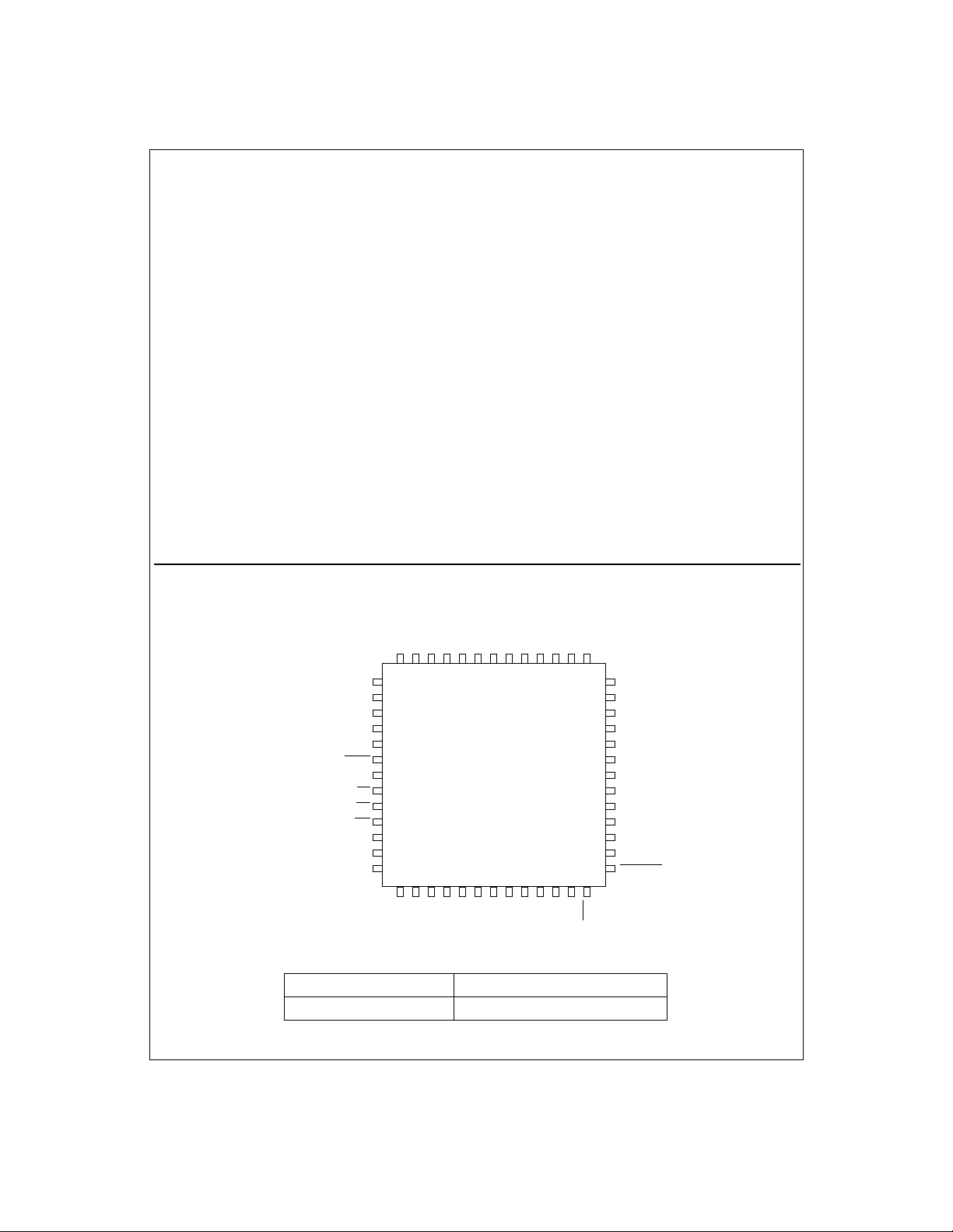
Ordering Information
Commercial (0°C ≤ TA ≤ +70°C) Package
LM9812CCV V52A 52 Pin Plastic Leaded Chip Carrier
TRI-STATE® is a registered trademark of National Semiconductor Corporation.
©1997 National Semiconductor Corporation
1
http://www.national.com
Page 2
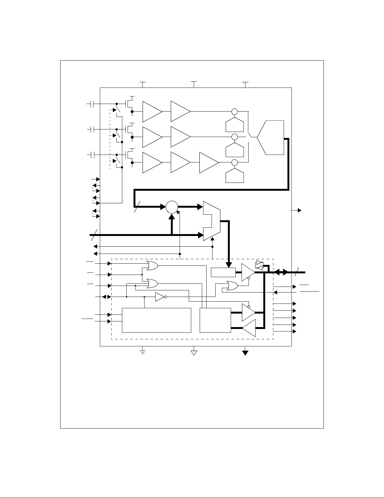
Block Diagram
RED OS
from Sensor
GREEN OS
from Sensor
BLUE OS
from Sensor
V
REF IN
V
REF LO OUT
V
REF LO IN
V
REF MID OUT
V
REF MID IN
V
REF HI OUT
V
REF HI IN
Gain/Offset
Coefficients
CD0-CD9
GCLK
SYNC
MCLK
RUN/STOP
OCLK
WR
CS
RD
OS
OS
OS
10
R
G
B
CLAMP
V
A
Coarse Color
Balance PGAs
CDS
CDS
CDS
x1-x3
x1-x3
x1-x3
Pixel-Rate Offset Subtractor
+
10 bits
+
-
Control
Logic
V
D
Blue Gain
x1or x3
Boost
Pixel-Rate
Shading Multiplier
Pixel Data
Latch
Configuration
Register
Static
Offset
DACs
+
²
+
Offset
DAC
+
²
+
Offset
DAC
+
²
+
Offset
DAC
V
DI/O
R
10-Bit,
6MHz
ADC
G
B
TEST
Pixel Data Output/
Control Data I/O
10
D0-D9
EOC
RD PIXEL
ø1
ø2
RS
TR1
TR2
AGND
DGND
2
DGND
I/O
http://www.national.com
Page 3
Absolute Maximum Ratings
Positive Supply Voltage (V+=VA=VD=V
With Respect to GND=AGND=DGND=DGND
Voltage On Any Input or Output Pin 0.3V to V
DI/O
(Notes 1 & 2)
)
I/O
+
+0.3V
Input Current at any pin (Note 3) ±25mA
Package Input Current (Note 3) ±50mA
Package Dissipation at T
ESD Susceptibility (Note 5)
= 25°C (Note 4)
A
Human Body Model 2000V
Soldering Information
Infrared, 10 seconds (Note 6) 300°C
Storage Temperature -65°C to +150°
Operating Ratings
Operating Temperature Range T
6.5V
LM9812CCV 0°C≤T
V
Supply Voltage +4.75V to +5.25V
A
V
Supply Voltage +4.75V to +5.25V
D
V
Supply Voltage +3.0V to +5.25V
DI/O
|V
|
A-VD
V
A-VDI/O
OS
, OSG, OSB, V
R
Input Voltage Range -0.05V to V
CD0-CD9, D0-D9, MCLK, SYNC,
RUN/STOP
REF IN
, CS, RD, WR, RD PIXEL
(Notes 1 & 2)
Input Voltage Range -0.05V to V
≤
MIN
≤
< -100mV
A
DI/O
Electrical Characteristics
The following specifications apply for AGND=DGND=DGND
f
=24MHz, Rs=25Ω. Boldface limits apply for T
MCLK
=0V, VA=VD=+5.0V
I/O
A=TJ=TMIN
to T
; all other limits TA=TJ=25°C. (Notes 7, 8, & 12)
MAX
CCD/CIS Source Requirements for Full Specified Accuracy and Dynamic Range (Note 12)
Color Balance PGA gain = 0.933
V
OS PEAK
Sensor’s Maximum Peak Differential
Signal Range
Color Balance PGA gain = 3.0
Color Balance PGA gain = 9.0
(Blue Channel, BOOST on)
Sensor’s Maximum Correctable Range
of Pixel-to-Pixel V
Variation/Color
WHITE
Range 0
Range 1
Range 2
Coarse Color Balance PGA Characteristics
Monotonicity 5 bits (min)
G
(Minimum PGA Gain) PGA Setting = 0 0.93
0
G
(Maximum PGA Gain) PGA Setting = 31 3.00
31
G
BLUE BOOST
Blue PGA Boost Setting = x3 3.00
Gain Error at any gain (Note 14) ±1.0 ±4.0
Static Offset DAC Characteristics
Monotonicity 6 bits (min)
Offset DAC LSB size In units of ADC LSBs 4.2
Offset DAC Adjustment Range In units of ADC LSBs ±130 ±118 LSB (min)
ADC Characteristics
Resolution with No Missing Codes 10 Bits (min)
ILE Integral Linearity Error (Note 11) ±0.4 ±1.5 LSB (max)
DNL Differential Non-Linearity
System Characteristics
C Analog Channel Gain Constant 2.00
, V
=+5.0 or +3.3VDC, V
DC
DI/O
-0.14
+0.32
REF IN
1.0
0.33
0.11
67 (1:3)
50 (1:2)
33 (1:1.5)
0.90
0.97
2.85
3.20
2.72
3.27
1.3
7.2
-0.5
+1.0
1.83
2.17
= +2.0VDC,
≤
T
T
A
MAX
≤
+70°C
A
100mV
+ 0.05V
+ 0.05V
V (min)
V (min)
V (min)
%
%
%
V/V (max)
V/V (min)
V/V (max)
V/V (min)
V/V (max)
V/V (min)
% (min)
% (max)
LSB (min)
LSB (max)
LSB (min)
LSB (max)
(min)
(max)
3
http://www.national.com
Page 4
Electrical Characteristics
The following specifications apply for AGND=DGND=DGND
f
=24MHz, Rs=25Ω.
MCLK
V
V
V
Pre-PGA Analog Channel Offset Error
OS1
CCD Mode
Pre-PGA Analog Channel Offset Error
OS1
CIS Mode
Post-PGA Analog Channel Offset Error In units of ADC LSBs -5
OS2
Boldface limits apply for T
(Continued)
V
V
=0V,
=
I/O
A=TJ=TMIN
=
A
D
to T
; all other limits TA=TJ=25°C. (Notes 7, 8, & 12)
MAX
In units of ADC LSBs +5
In units of ADC LSBs +32
Reference and Analog Input Characteristics
OS
, OSG, OSB Input Capacitance 5 pF
R
OS
, OSG, OSB Input Leakage Current Measured with OS = 2.5V
R
V
Input Leakage Current Measured with V
REF IN
REF IN
DC and Logic Electrical Characteristics
V
The following specifications apply for AGND=DGND=DGND
f
=24MHz, Rs=25Ω.
MCLK
Boldface limits apply for T
I/O
A=TJ=TMIN
Symbol Parameter Conditions
D0-D9, CD0-CD9, MCLK, RUN/STOP
V
V
C
D0-D9, EOC
V
OUT(1)
V
OUT(0)
I
OUT
Logical “1” Input Voltage
IN(1)
Logical “0” Input Voltage
IN(0)
I
Input Leakage Current
IN
Input Capacitance 5 pF
IN
, GCLK, OCLK, SYNC Digital Output Characteristics
Logical “1” Output Voltage
Logical “0” Output Voltage
TRI-STATE® Output Current
(D0-D9 only)
, SYNC, CS, RD, WR, RD PIXEL Digital Input Characteristics
V
DI/O
V
DI/O
V
DI/O
V
DI/O
V
=V
IN
VIN=DGND
V
DI/O
V
DI/O
V
DI/O
V
DI/O
V
DI/O
V
DI/O
V
OUT
V
OUT
Ø1, Ø2, RS, TR1, TR2 Digital Output Characteristics
V
=4.75V, I
V
V
OUT(1)
OUT(0)
Logical “1” Output Voltage
Logical “0” Output Voltage VD=5.25V, I
D
V
=4.75V, I
D
Power Supply Characteristics
Analog Supply Current
I
A
I
Digital Supply Current
D
Operating
Standby
Operating
Standby
V
=0V,
=
=
A
D
to T
; all other limits TA=TJ=25°C. (Notes 7 & 8)
MAX
=5.25V
=3.6V
=4.75V
=3.0V
D
=4.75V, I
OUT
=4.75V, I
OUT
=3.0V, I
=3.0V, I
=5.25V, I
=3.6V, I
OUT
OUT
OUT
OUT
=-360µA
=-10µA
=1.6mA
=DGND
=V
D
=-360µA
OUT
=-10µA
OUT
=1.6mA
OUT
+5.0
V
= 2.0V
+5.0
V
=-360µA
=-10µA
=1.6mA
, V
=+5.0 or +3.3VDC, V
DC
DI/O
DC
DC
, V
=+5.0 or +3.3VDC, V
DC
DI/O
2
4
Typical
(Note 9)
0.1
-0.1
0.1
-0.1
60
7
4.7
0.1
REF IN
-40
+40
-65
+135
-40
+30
20
20
REF IN
Limits
(Note 10)
2.0
2.0
0.8
0.7
2.4
4.4
2.1
2.5
0.4
0.4
2.4
4.4
0.4
85
10
10
1.0
= +2.0VDC,
LSB (min)
LSB (max)
LSB (min)
LSB (max)
LSB (min)
LSB (max)
nA (max)
nA (max)
= +2.0VDC,
Units
(Limits)
V (min)
V (min)
V (max)
V (max)
µA
µA
V (min)
V (min)
V (min)
V (min)
V (max)
V (max)
µA
µA
V (min)
V (min)
V (max)
mA (max)
mA (max)
mA (max)
mA (max)
4
http://www.national.com
Page 5
DC and Logic Electrical Characteristics
The following specifications apply for AGND=DGND=DGND
f
=24MHz, Rs=25Ω.
MCLK
Boldface limits apply for T
A=TJ=TMIN
I/O
(Continued)
V
V
=0V,
to T
+5.0
=
=
A
D
; all other limits TA=TJ=25°C. (Notes 7 & 8)
MAX
Symbol Parameter Conditions
I
DI/O
Digital I/O Supply Current
Operating, V
Standby, V
Operating, V
Standby, V
DI/O
DI/O
DI/O
= 5.0V
DI/O
= 3.3V
=5.0V
=3.3V
AC Electrical Characteristics, MCLK Independent
V
V
The following specifications apply for AGND=DGND=DGND
, tr=tf=5ns
=1/f
t
MCLK
MCLK
Boldface limits apply for T
, R
=25¾, CL (databus loading) = 50pF/pin.
s
A=TJ=TMIN
to T
; all other limits TA=TJ=25°C. (Notes 7 & 8)
MAX
I/O
=0V,
Symbol Parameter Conditions
f
MCLK
Maximum MCLK Frequency
Minimum MCLK Frequency
MCLK Duty Cycle
t
SETUP (OUT)
t
HOLD (OUT)
t
SETUP (IN)
t
HOLD (IN)
t
GCLK-EOC
Coefficient Data valid before latching
edge of OCLK or GCLK
Coefficient Data held after latching
edge of OCLK or GCLK
Coefficient Data Valid before latching
edge of OCLK or GCLK
Coefficient Data held after latching
edge of OCLK or GCLK
Rising edge of GLCK to falling edge
of EOC
(GCLK as output)
GCLK and OCLK as
outputs
GCLK and OCLK as
outputs
GCLK and OCLK as
inputs
GCLK and OCLK as
inputs
Rising edge of GLCK to falling edge
t
GCLK-OCLK
t
EOC-OCLK
t
OCLK-GCLK
of OCLK (GCLK and OCLK as
outputs)
Rising edge of EOC to rising edge of
OLCK (OCLK as output)
Rising edge of OLCK to falling edge
of GLCK (GCLK and OCLK as
2 bus / 2 clock mode 1 ns
2 clock mode 1 ns
2 clock mode 3 ns
outputs)
t
EOC-GCLK
t
DACC
t
D1H, D0H
t
CS SETUP
t
CS HOLD
t
WR SETUP
Rising edge of EOC to falling edge of
GLCK (GCLK as output)
RD or RD_PIXEL low to D0-D9 data
valid
RD or RD_PIXEL high to D0 - D 9 da ta
tri-state
CS setup of RD or WR
CS hold after RD or WR
D0-D9 data valid before rising edge
of WR
(setup time)
2 bus mode 2 ns
V
=
=
A
D
V
DI/O
, V
=+5.0 or +3.3VDC, V
DC
DI/O
=+5.0
V
DC
Typical
(Note 9)
12
-10
0
0
,
V
Typical
(Note 9)
12
5
2
0.3
REF IN
= +2.0VDC, f
Limits
(Note 10)
24
4
40
60
20
0
5
5
REF IN
Limits
(Note 10)
30
20
10
3
MCLK
= +2.0VDC,
Units
(Limits)
mA (max)
mA (max)
mA (max)
mA (max)
=24MHz
Units
(Limits)
MHz (min)
MHz (max)
% (min)
% (max)
ns (min)
ns (min)
ns (min)
ns (min)
,
2ns
15
13
41
20
0
0
5
ns (max)
ns (max)
ns (min)
ns (min)
ns (min)
5
http://www.national.com
Page 6
AC Electrical Characteristics, MCLK Independent
The following specifications apply for AGND=DGND=DGND
, tr=tf=5ns
=1/f
t
MCLK
MCLK
Boldface limits apply for T
, R
=25¾, CL (databus loading) = 50pF/pin.
s
A=TJ=TMIN
to T
; all other limits TA=TJ=25°C. (Notes 7 & 8)
MAX
I/O
=0V,
Symbol Parameter Conditions
t
WR HOLD
D0-D9 data valid after rising edge of
WR
(hold time)
V
=
A
=+5.0
V
V
=
D
DI/O
AC Electrical Characteristics, MCLK Dependent
The following specifications apply for AGND=DGND=DGND
=1/f
t
MCLK
MCLK
labeled C.R.
, tr=tf=5ns
Boldface limits apply for T
, R
=25Ω, CL (databus loading) = 50pF/pin. Refer to Table 2: Configuration Register Parameters for limits
s
A=TJ=TMIN
to T
=0V,
I/O
; all other limits TA=TJ=25°C. (Notes 7 & 8)
MAX
Symbol Parameter Conditions
t
R/S START
t
START
t
SYNC END
Rising edge of RUN/STOP to Rising
edge of SYNC
Rising edge of SYNC to rising edge
of TR1
Falling edge of SYNC to last rising
edge of EOC
SYNC OUT mode
SYNC IN mode
SYNC IN mode
SYNC OUT mode
SYNC IN mode
SYNC OUT mode
SYNC IN mode
t
SYNC LOW
t
TR1 WIDTH
t
TR2 WIDTH
t
GUARD
t
RS WIDTH
t
CLAMP ON
t
CLAMP OFF
t
t
RS
t
HOLD REF
t
HOLD SIG
t
OCLK LOW
t
OCLK HIGH
t
GCLK LOW
t
GCLK HIGH
SYNC low time
,
TR1, TR2 Transfer Pulse Width
TR1, TR2 Transfer Pulse Guardband
Reset Pulse Width
Start of Optical Black clamping
period
End of Optical Black clamping period
Ø1, Ø2 clock period
Ø
RS pulse position from Ø1 edge
Reference hold (sample) position
from RS edge
Signal hold (sample) position from
RS edge
OCLK low time (OCLK as Output)
OCLK high time (OCLK as Output)
GCLK low time (GCLK as Output)
GCLK high time (GCLK as Output)
SYNC OUT mode
Standard Mode
Even/Odd Mode
2 bus mode
1bus mode
2 bus mode
1 bus mode
2 bus mode
1 bus mode
2 bus mode
1 bus mode
V
=
A
=+5.0
V
V
=
D
DI/O
(Continued)
V
DC
Typical
(Note 9)
V
DC
Typical
(Note 9)
t
1+
GUARDBAND
t
13+
GUARDBAND
t
GUARDBAND
8
0
,
,
V
REF IN
V
REF IN
= +2.0VDC, f
Limits
(Note 10)
0
= +2.0VDC, f
Limits
(Note 10)
16
t
GUARDBAND
14+
t
GUARDBAND
t
GUARDBAND
9
0
8
# of EOL
PIxels - 4
C.R.
C.R.
C.R.
C.R.
C.R.
12
24
C.R.
C.R.
C.R.
2*t
MCLK
1*t
MCLK
2*t
MCLK
3*t
MCLK
2*t
MCLK
1*t
MCLK
2*t
MCLK
3*t
MCLK
MCLK
MCLK
MCLKs (max)
MCLKs (min)
MCLKs (max)
MCLKs (max)
MCLKs (max)
MCLKs (min)
Pixel periods
=24MHz
Units
(Limits)
ns (min)
=24MHz
Units
(Limits)
MCLKs
MCLKs
MCLKs
MCLKs
MCLKs
MCLKs
MCLKs
MCLKs
MCLKs
MCLKs
MCLKs
ns
ns
ns
ns
,
,
6
http://www.national.com
Page 7
AC Electrical Characteristics, MCLK Dependent
V
V
=0V,
The following specifications apply for AGND=DGND=DGND
t
MCLK
labeled C.R.
, tr=tf=5ns
=1/f
MCLK
Boldface limits apply for T
, R
=25Ω, CL (databus loading) = 50pF/pin. Refer to Table 2: Configuration Register Parameters for limits
s
A=TJ=TMIN
I/O
to T
; all other limits TA=TJ=25°C. (Notes 7 & 8)
MAX
Symbol Parameter Conditions
t
EOC LOW
t
EOC HIGH
t
DATA VALID
EOC low time
EOC high time
D0-D9 data valid from falling
Read Phase = 0°)
Phase = 180°)
edge of EOC
or rising
(Data Read
(Data
=
A
D
V
=
(Continued)
=+5.0
DI/O
,
V
DC
Typical
(Note 9)
V
REF IN
= +2.0VDC, f
Limits
(Note 10)
2*t
MCLK
2*t
MCLK
4*t
-20ns
MCLK
MCLK
=24MHz
Units
(Limits)
ns
ns
ns (min)
,
OCLK rising edge to EOC falling edge
t
t
OCLK-EOC 1
(OCLK IN)
(Gain Coefficient Write Phase = 0°),
OCLK falling edge to EOC falling edge
(Gain Coefficient Write Phase = 180°)
1 bus mode w/ext OCLK
MCLK
4*t
+ 40ns
MCLK
ns (min)
ns (max)
OCLK rising edge to EOC rising edge
t
OCLK-EOC 2
(OCLK IN)
(Gain Coefficient Write Phase = 0°),
OCLK falling edge to EOC rising edge
(Gain Coefficient Write Phase = 180°)
2 bus mode w/ext OCLK
3*t
40ns
MCLK
ns (min)
ns (max)
GCLK rising edge to EOC falling edge
t
GCLK-EOC
(GCLK IN)
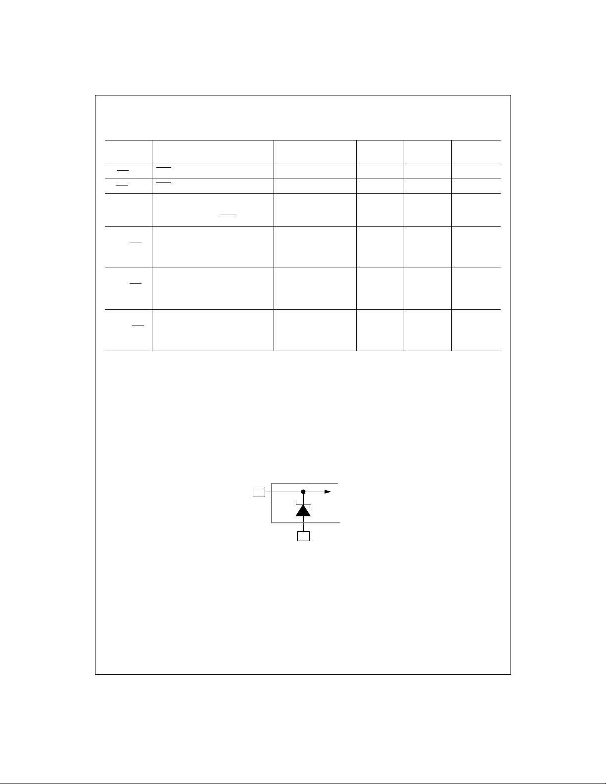
Note 1: Absolute Maximum Ratings indicate limits beyond which damage to the device may occur. Operating Ratings indicate conditions for which the device is functional,
but do not guaran te e specific performance limits. For guarante ed specifications and test conditio ns, s ee the Electrical Characteristics. Th e guaranteed spec if ic at ions apply
only for the test conditio ns lis t ed. Some performance c haracteristics may degrade w hen the device is not operated under the listed test conditions.
Note 2: All voltages are measured with respect to GND=AGND=DGND=DGND
Note 3: When the input voltage (V
imum package input cu rrent rating limits the numb er of pins that can simultaneously safely exceed the power supplies with an input current of 25mA to two.
Note 4: The maximum powe r dissipa tion must be de rated at elevated temp eratur es and is dicta ted by T
able power dissipatio n at any temperature is P
is 52°C/W for the V52A PLCC package
Note 5: Human body model, 100pF capacitor discharged through a 1.5kΩ resistor.
Note 6: See AN450 “Surface Mounting Methods and Their Effect on Product Reliability” or the section ti tl ed “Surface Mount” found in any post 1986 National Semiconduc-
tor Linear Data Book for other methods of solder ing surface mount devices.
Note 7: A Zener diode c lamps the OS an alog inputs to AGND as shown below. This input prote ction, in combin ation with the exter nal clamp capaci tor and the outpu t
impedance of the se ns or, prevents dam age to the LM9812 fro m tran s ients during power-up.
(Gain Coefficient Write Phase = 0°),
GCLK falling edge to EOC falling edge
(Gain Coefficient Write Phase = 180°)
) at any pin exceeds the power supplies (VIN<GND or VIN>VA or VD), the current at that pin should be limited to 25mA. The 50mA max-
IN
= (TJmax - TA) / ΘJA. TJmax = 150°C for this device. The typical thermal resistance (ΘJA) of this part when board mounted
D
.
w/ext GCLK
=0V, unless otherwise specified.
I/O
max, ΘJA and the ambie nt temperature, TA. The maximum allow-
J
3*t
40ns
MCLK
ns (min)
ns (max)
OS Input
AGND
Note 8: To guarantee accuracy, it is required that V
Note 9: Typicals are at T
Note 10: Tested limits are guaranteed to Na t ional's AOQL (Average Outgoing Qualit y Level).
Note 11: Integral linearity error is defined as the deviation of the analog value, expressed in LSBs, from the straight line that best fits the actual transfer function of the ADC.
Note 12: V
a white (full scale) image with respect to the reference level, V
correctable range o f pixel-to-pixel V
is defined as the CCD OS voltage for the reference period f ollowing the reset feedthrough pulse. V
REF
J=TA
=25°C, f
MCLK
WHITE
and VD be connected together to the same power supply w it h s eparate bypass capacito rs at eac h supply pin.
A
= 24MHz, and represent most likely parametric norm.
is defined as the peak positive deviation above V
. V
REF
variation is defi ned as the maxim um variation in V
RFT
7
To Internal
Circuitry
is defined as the peak CCD pixel output voltage for
WHITE
of the reset feedthrough pulse. The maximum
(due to PRNU, light source intensity variation, optics, etc.) that the
WHITE
REF
http://www.national.com
Page 8
LM9812 can correc t for using its internal PGA.
CCD Output Signal
V
RFT
V
Note 13: Reference voltages below 1.80V may decreas e SNR. Reference voltages above 2.20V may cause linearity (headroom) errors inside the LM9812. The
LM4041DIM3-A D J (SOT-23 package) or the LM4041DIZ-ADJ (TO-92 package) bandgap voltage references are recommended for this application.
Note 14: PGA Gain Error is the maximum difference between the measured gain for any PGA code and the ideal gain calculated by using the formula
V
--- -
Gain
PGA
V
PGA code
G0X
---------------- ---------- -+=XG
where .
32
32
–()
------=
31G0
31
V
REF
WHITE
8
http://www.national.com
Page 9
Pin Descriptions
Sensor Driver Signals
ø1 Digital Output. Clock signal, phase 1.
ø2 Digital Output. Clock signal, phase 2.
RS Digital Output. Reset pulse.
TR1, TR2 Digital Output. Transfer pulses.
Analog I/O
OSR, OSG,
OS
,
B
V
REF IN
V
REF LO OUT,
V
REF LO IN
V
REF MID OUT,
V
REF MID IN
V
REF HI OUT,
V
REF HI IN
Analog Inputs. These inputs (for Red, Green,
and Blue) should be tied to the sensor’s OS
(Output Signal) through DC blocking capacitors.
Analog Input. This is the system reference voltage input and should be connected to a 2.0V
voltage source and bypassed to AGND wi th a
0.05µF monolithic capacit or.
Analog Output/Input. V
equal to 0.49V
=2V) developed by the LM9812. It should be
IN
tied to V
REF LO IN
a 0.05µF monolithic capacitor.
Analog Output/Input. V
equal to 0.49V
oped by the LM9812. It should be tied to V
and bypassed to AGND with a 0.05µF
MID IN
monolithic capacitor.
Analog Output/Input. V
equal to 0.49V
=2V) developed by the LM9812. It should be
IN
tied to V
REF HI IN
0.05µF monolithic capacit or.
REF LO OUT
- V
A
REF IN
and bypassed to AGND with
REF MID OUT
(2.45V for V
A
REF HI OUT
+ V
A
REF IN
and bypassed to AGND with a
is a voltage
/2 (1.45V for V
is a voltage
=2V) devel-
REF IN
is a voltage
/2 (3.45V for V
REF
REF
Configuration Register I/O
CS Digital Input. This is the Chip Select signal for
RD
WR
reading or writing to the Configuration Register
through the D0-D9 databus. This input must be
low in order to enable writing to or reading from
the Configuration Register.
Digital Input. A low signal on this input, when
SYNC and CS
the currently addressed Configuration Register on the D0-D9 databus. A RD
resets the internal address latching state
machine. NOTE: If this pin is taken low when
CS is high, the D0-D9 databus will come out of
tri-state and drive random data onto the bus.
Digital Input. This input, when simultaneously
asserted along with CS
the D0-D9 databus to the LM9812. If this is the
first write in the cycle, this data is the address
to be read or written to. If this is the second
write in the cycle, this data is the data to be
written to the Configuration Register at the currently latched address. Writing to the Configuration Register is independent of the state of
SYNC.
are also low, pl aces the data in
cycle also
, transfers the data on
REF
General Digital I/O
MCLK Digital Input. This is the 24MHz (typical) master
SYNC Digital Input (SYNC_IN mode) /
RUN/STOP
system clock.
Digital Output (SYNC_OUT mode).
In the SYNC_IN mode, a low-to-high transition
on this input begins a line scan operation. The
line scan operation terminates when SYNC is
taken low. In the SYNC_OUT mode, the rising
edge of this output indicates the start of a line
of data and the falling edge indicates the end of
a line of data.
Digital Input. In the SYNC_OUT mode, this
input should be taken high to begin converting
a series of lines, and taken low to stop converting a series of lines. In the SYNC_IN mode this
input is ignored.
Digital Coefficient I/O
CD0 (LSB) CD9 (MSB)
OCLK Digital Input/Output. This is the signal that is
GCLK Digital Input/Output. This is the signal that is
Digital Inputs. This is the 10 bit data path for
the pixel-rate gain coefficient and offset data.
used to clock the Offset coefficients into the
LM9812 through the CD0-CD9 databus. This
can be either an output or an input depending
on the state of bit 7 of Register 9. D ata is
latched on the rising edge of OCLK.
used to clock the Shading (gain) coefficients
into the LM9812 through the CD0-CD9 databus. Th is can be either an outpu t or an input
depending on the state of bit 7 of Register 9.
Data is latched on the rising edge of GCLK.
Digital Output I/O
D0 (LSB)D9 (MSB)
EOC
RD PIXEL
Digital Inputs/Outputs. When SYNC is high and
RD PIXEL
bit digital output data during line scan. This
databus is also used for reading or writing to
the Configuration Register using the RD
and CS
Register can occur at any time. Reading from
the Configuration Register can only occur
when SYNC is low.
Digital Output. This is the End Of Conversion
signal from the LM9812 indicating that new
pixel data is available on the D0-D9 databus.
Digital Input. When SYNC is high, taking this
input low places the digital pixel data stored in
the output latch onto the D0-D9 bus. This input
is ignored when SYNC is low.
is low, this data bus outputs the 10
, WR
signals. Writing to the Configuration
Test
TEST Analog Output. This pin can be used to view
the CDS and Clamp signals. See Register 27,
bits 6 and 7.
9
http://www.national.com
Page 10
Analog Power
V
A
AGND This is the ground return for the analog supply.
This is the positive supply pin for the analog
supply. It should be connected to a voltage
source of +5V and bypassed to AGND with a
0.1µF monolithic capacitor in parallel with a
10µF tantalum capacitor.
Digital Power
V
D
DGND This is the ground return for the digital supply.
V
DI/O
DGND
This is the positive supply pin for the digital
supply. It should be connected to a voltage
source of +5V and bypassed to DGND with a
0.1µF monolithic capa citor.
This is the positive supply pin for the digital
supply for the LM9812’s I/O. It should be connected to a voltage source of +3V to +5V and
bypassed to DGND
capacitor. If the supply for this pin is different
than the supply for V
bypassed with a 10µF tantalum capacitor.
This is the ground return for the digital supply
I/O
for the LM9812’s I/O.
with a 0.1µF monolithic
I/O
and VD, it should also be
A
10
http://www.national.com
Page 11
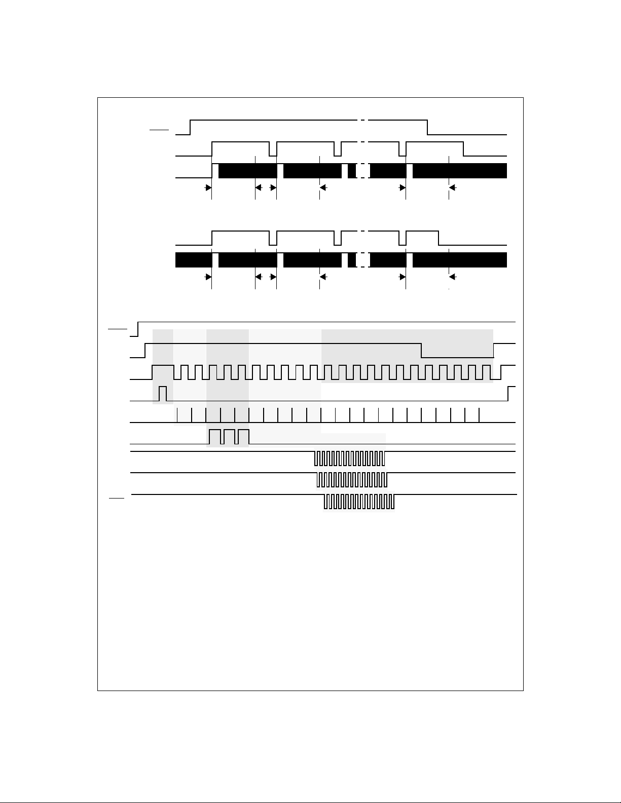
Timing Diagrams
RUN/STOP
SYNC (OUTPUT)
Ø1
SYNC (INPUT)
Ø1
RUN/
STOP
SYNC
(OUTPUT)
Ø1
TR1
Transfer
Dummy Black Valid Pix els
Line 1
Diagram 1: SYNC OUT Mode Timing, Multiple Lines
Line 1
Diagram 2: SYNC IN Mode Timing, Multiple Lines
Line 2 Line n
Line 2 Line n
Additional Integration Time
(truncated)
RS
CLAMP
OCLK
GLCK
EOC
123
Diagram 3: SYNC OUT Mode Timing, One Line
11
http://www.national.com
Page 12
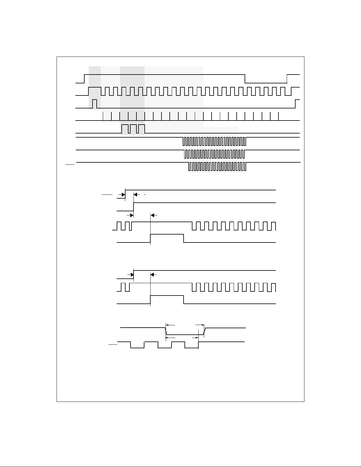
SYNC
(INPUT)
Ø1
TR1
RS
Transfer
Dummy Black Valid Pix els
CLAMP
OCLK
GLCK
EOC
RUN/STOP
SYNC (OUTPUT)
Ø1
TR1
SYNC (INPUT)
Ø1
TR1
123
Diagram 4: SYNC In Mode Timing, One Line
t
R/S START
t
START
Diagram 5: Start of Line Scan, SYNC OUT Mode, One TR Pulse
t
START
Diagram 6: Start of Line Scan, SYNC IN Mode, One TR Pulse
t
SYNC LOW
SYNC
t
SYNC END
8MCLK max
EOC
Diagram 7: Timing for End of Line/Start of Next Line
12
8MCLK min
http://www.national.com
Page 13

TR1 (TR1 Polarity = 0)
TR1 (TR1 Polarity = 1)
TR1 (TR1 Polarity = 0)
t
TR1 WIDTH
t
t
GUARD
GUARD
Ø1
Ø2
Diagram 8: TR Pulse Timing, One TR Pulse
t
TR1 WIDTH
RS
OS
Clamp Signal
(Internal)
TR1 (TR1 Polarity = 1)
TR1 (TR2 Polarity = 0)
TR2 (TR2 Polarity = 1)
RS (RS Polarity = 0)
RS (RS Polarity = 1)
t
GUARD
t
GUARD
t
GUARD
t
TR2 WIDTH
t
GUARD
Ø1
Ø2
Diagram 9: TR Pulse Timing, Two TR Pulses
t
RS WIDTH
Diagram 10: RS Pulse Polarity
nn+1n-1
nn+1n-1
t
CLAMP ON
nn-1
t
CLAMP OFF
Diagram 11: CCD Clamping Timing
13
http://www.national.com
Page 14

Ø1
(Even/Odd Mode)
Ø2
(Even/Odd Mode)
Ø1
(Standard Mode)
Ø2
(Standard Mode)
RS
t
RS WIDTH
t
Ø
t
Ø
t
RS
nn+1n-1
OS
CDS
(Internal)
Hold Ref
(n-1)
Ø1(Std Mode)
Ø2 (Std Mode)
Ø1(Even/Odd)
Ø2 (Even/Odd)
RS
OS
CDS
Clamp
Note:
i = value programmed in Dummy Pixel Register
j = value programmed in Optical Black Register
Diagram 13: Dummy Pixel and Optical Black Pixel Timing
t
HOLD REF
Hold Signal
(n-1)
Diagram 12: CDS Ti ming
pixel 1
(dummy)
nn+1n-1
t
HOLD SIG
Hold Ref
(n)
pixel i pixel i +1
(dummy)
Hold Signal
(black)
(n)
Hold Ref
pixel i +j
(black)
(n-1)
(data)
14
http://www.national.com
Page 15

OCLK (from LM9812)
GCLK (from LM9812)
CD0-CD9
B Gain
n-1
t
GCLK-EOC
R Off
n
t
SETUP
t
HOLD
R Gain
t
GLCK-OCLK
t
SETUP
n
t
HOLD
G Off
n
t
OCLK-GCLK
G Gain
n
EOC
D0-D9
G Output Data
n-1
B Output Data
t
EOC-OCLK
n-1
Diagram 14: Digital Data Timing, Output Data and Coefficient Data on separate buses, two clocks
(OCLK and GCLK) for coefficient data, OCLK and GCLK generated by LM9812, RD PIXEL held low.
t
SETUP
t
HOLD
GCLK (from LM9812)
t
CD0-CD9
EOC
D0-D9
B Gain
t
GCLK-EOC
n-1
G Output Data
R Off
n
t
EOC-GCLK
n-1
R Gain
SETUP
n
B Output Data
t
HOLD
G Off
n
n-1
G Gain
Diagram 15: Digital Data Timing, output data and coefficient data on separate buses, one clock
(GCLK) for coefficient data, GCLK generated by LM9812, RD PIXEL
t
SETUP
t
HOLD
held low.
t
OCLK-GCLK
OCLK (from LM9812)
GCLK (from LM9812)
t
SETUP
t
HOLD
t
EOC-OCLK
CD0-CD9
B Gain
n-1
R Offset
n
R Gain
n
G Gain
n
G Offset
EOC = RD PIXEL
n
t
GCLK-EOC
n
R Gain
B Output Data
B Output Data
n
n-1
n-1
G Off
n
D0-D9
EXTERNAL DATABUS
G Output Data
G Output Data
n-1
n-1
R Off
n
Diagram 16: Digital Data Timing, output data and coefficient data on same buses, two clocks
(OCLK and GCLK) for coefficient data, OCLK and GCLK generated by LM9812.
15
R Out
B Gain
R Out
n
http://www.national.com
n
n
Page 16

GCLK (from LM9812)
CD0-CD9
EOC = RD PIXEL
D0-D9
EXTERNAL DATABUS
B Gain
t
GCLK-EOC
n-1
G Output Data
G Output Data
n-1
n-1
R Offset
R Off
n
t
SETUP
t
HOLD
R Gain
n
R Gain
n
B Output Data
B Output Data
n
n-1
n-1
G Offset
G Off
n
G Gain
n
G Gain
n
t
SETUP
t
n
R Out
R Out
HOLD
n
n
Diagram 17: Digital Data Timing, output data and coeffi cient data on same buses, one clock
(GCLK) for coefficient data, GCLK generated by LM9812.
t
SETUP
t
HOLD
OCLK (to LM9812)
GCLK (to LM9812)
t
R Gain
n
SETUP
t
HOLD
G Off
n
B Output Data
G Gain
t
OCLK-EOC 2 (OCLK IN)
n-1
n
t
GCLK-EOC (GCLK IN)
CD0-CD9
EOC
D0-D9
B Gain
n-1
R Off
n
G Output Data
n-1
Diagram 18: Digital Data Timing, output data and coefficient data on separate buses, two clocks (OCLK and
GCLK) for coefficient data, OCLK and GCLK input to LM9812, OCLK and GLCK phase = 0°, RD PIXEL
t
SETUP
t
HOLD
held low.
OCLK (to LM9812)
GCLK (to LM9812)
t
SETUP
t
HOLD
CD0-CD9
R Gain
n-1
G Off
n
G Gain
n
B Off
n
B Gain
n
EOC
t
GCLK-EOC (GCLK IN)
n-1
B Output Data
n-1
D0-D9
t
OCLK-EOC 2 (OCLK IN)
G Output Data
Diagram 19: Digital Data Timing, output data and coefficient data on separate buses, two clocks (OCLK and
GCLK) for coefficient data, OCLK and GCLK input to LM9812, OCLK and GLCK phase = 180°, RD PIXEL
16
http://www.national.com
held low.
Page 17

OCLK (to LM9812)
GCLK (to LM9812)
CD0-CD9
EOC
B Gain
t
SETUP
t
HOLD
t
SETUP
t
HOLD
n
R Gain
n
G Offset
G Gain
n
t
OCLK-EOC 1 (OCLK IN)
n
n-1
R Offset
t
GCLK-EOC (GCLK IN)
D0-D9
G Output Data
n-1
B Output Data
n-1
R Out
Diagram 20: Digital Data Timing, output data and coeffi cient data on same bus, two clocks (OCLK and
GCLK) for coefficient data, OCLK and GCLK input to LM9812, OCLK and GLCK phase = 0°.
t
SETUP
t
HOLD
OCLK (to LM9812)
GCLK (to LM9812)
t
SETUP
t
HOLD
CD0-CD9
R Gain
n-1
G Offset
G Gain
n
t
GCLK-EOC (GCLK IN)
n
B Offset
t
B Gain
n
OCLK-EOC 1 (OCLK IN)
n
EOC
D0-D9
G Output Data
n-1
B Output Data
n-1
R Out
Diagram 21: Digital Data Timing, output data and coeffi cient data on same bus, two clocks (OCLK and
GCLK) for coefficient data, OCLK and GCLK input to LM9812, OCLK and GLCK phase = 180°.
DATA (INTERNAL)
Green Internal Data
n-1
Blue Internal Data
n-1
EOC
t
RD PIXEL
D0-D9
DATAVALID
Green Output Data
n-1
t
DACC
B
n-1
B Output Data
t
D1H, tD0H
n-1
n
n
Diagram 22: RD PIXEL
Output Timing (Data Read Phase = 0°)
17
http://www.national.com
Page 18

DATA (INTERNAL)
EOC
RD PIXEL
D0-D9
Green Internal Data
t
DATAVALID
Green Output Data
n-1
n-1
Blue Internal Data
B
n-1
t
DACC
B Output Data
n-1
t
D1H, tD0H
n-1
Diagram 23: RD PIXEL
t
CS SETUP
Output Timing (Data Read Phase = 180°)
t
CS HOLD
t
CS SETUP
t
CS HOLD
CS
WR
t
WR SETUP
D0-D7
Note: To read from the Configuration Register, SYNC must be low, either by driving SYNC low (in SYN C IN mod e), or taking RUN/STOP low and waiting for SYNC to go low at the end of a line (in SYNC OUT mod e). T he Configuration Reg is t er c an be written to independent of the state of SYNC.
ADDRESS
t
WR HOLD
t
WR SETUP
DA TA
t
WR HOLD
Diagram 24: Writing to the Configuration Register, RD held high.
SYNC
t
CS SETUP
t
CS HOLD
t
CS SETUP
t
CS HOLD
CS
WR
RD
D0-D7
Note: To read from the Configuration Register, SYNC must be low, either by driving SYNC low (in SYNC IN mode), or taking RUN/STOP low and waiting for SYNC to go low at the end of a line (in SYNC OUT mode). The Configurat ion Register can be written to independe nt of th e stat e of SYNC.
t
WR SETUP
ADDRESS
t
WR HOLD
t
DACC
DATA
t
D1H, tD0H
Diagram 25: Reading the Configuration Register
18
http://www.national.com
Page 19

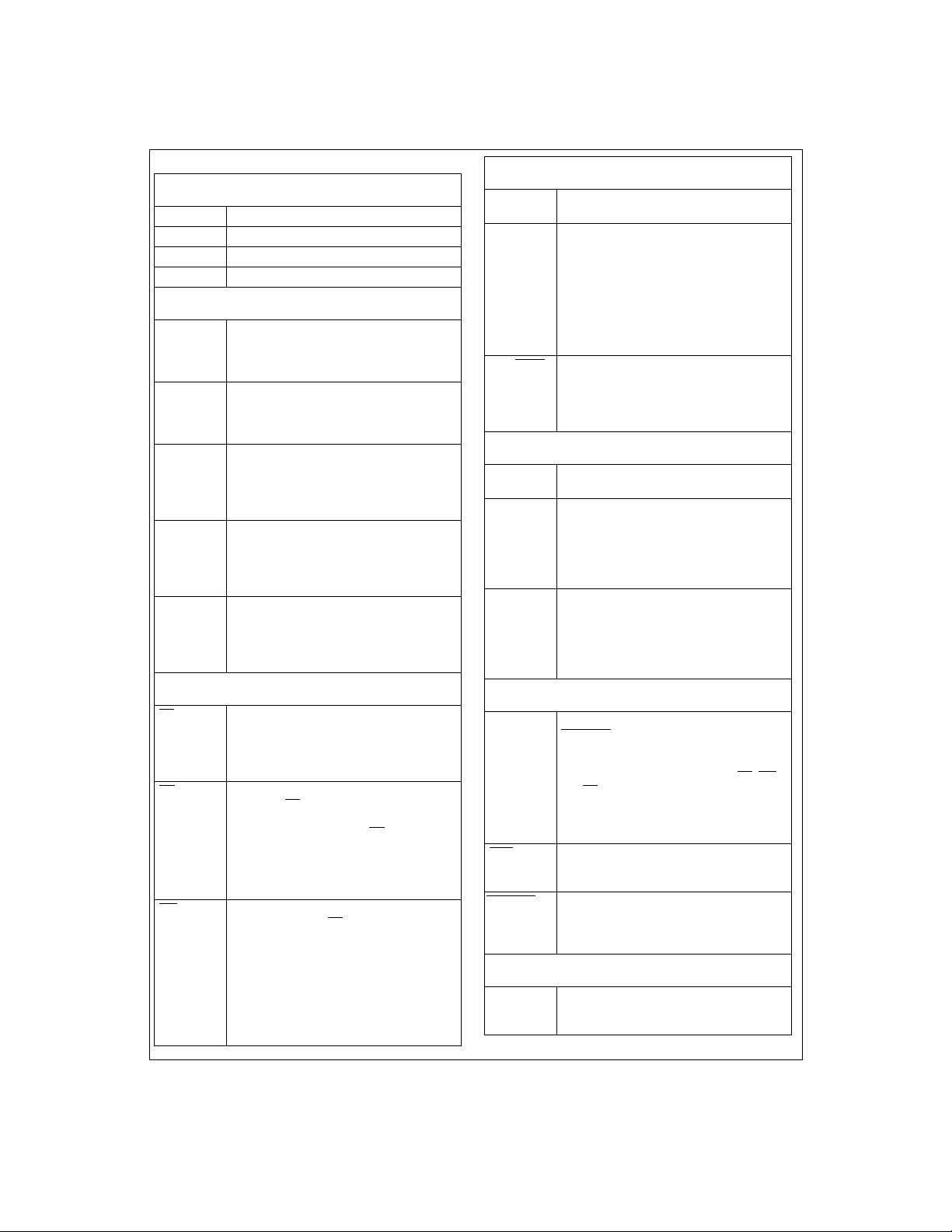
Table 1: Configuration Register Address Table
Address
(Decimal)
Address
(Binary)
A4 A3 A2 A1 A0 D7 D6 D5 D4 D3 D2 D1 D0
0 00000
1 00001
2 00010
3 00011
4 00100
5 00101
6 00110
7 00111
8 01000
9 01001
10 01010
11 01011
12 01100
13 01101
14 01110
15 01111
16 10000
17 10001
18 10010
19 10011
20 10100
Data Bits
Static Offset (Red)
- - Sign MSB LSB
Static Offset (Green)
- - Sign MSB LSB
Static Offset (Blue)
- - Sign MSB LSB
Coarse Color Balance PGA (Red)
---MSB LSB
Coarse Color Balance PGA (Green)
---MSB LSB
Coarse Color Balance PGA (Blue)
x3 - - MSB LSB
Internal Offset Subtractor Coefficient
MSB LSB
Internal Gain Multiplier Coefficient
LSB
Internal Gain Multiplier Coefficient (LM9812 only)
------MSB
Misc Group 1
Internal
External
Coefficient
Clock
MSB LSB
MSB LSB
--MSB
--MSB
--MSB LSB
--MSB LSB
--MSB LSB
---MSB LSB
---MSB LSB
Number of
Coefficient
-
Number of End of Line Integration Pixels (LSB)
Number of End of Line Integration Pixels (MSB)
Number of
Databusses
Clocks
in System
Number of Dummy Pixels
Number of Optical Black Pixels
Number of Active Pixels (LSB)
Number of Active Pixels (MSB)
TR1 Pulse Duration
TR2 Pulse Duration
TR1/TR2 Guardbands
Optical Black Clamp Start
Optical Black Clamp End
Multiplier
Gain Range
1
Multiplier
Gain Range
0
Multiplier
Coefficient
Source
Offset
Coefficient
Source
LSB
LSB
19
http://www.national.com
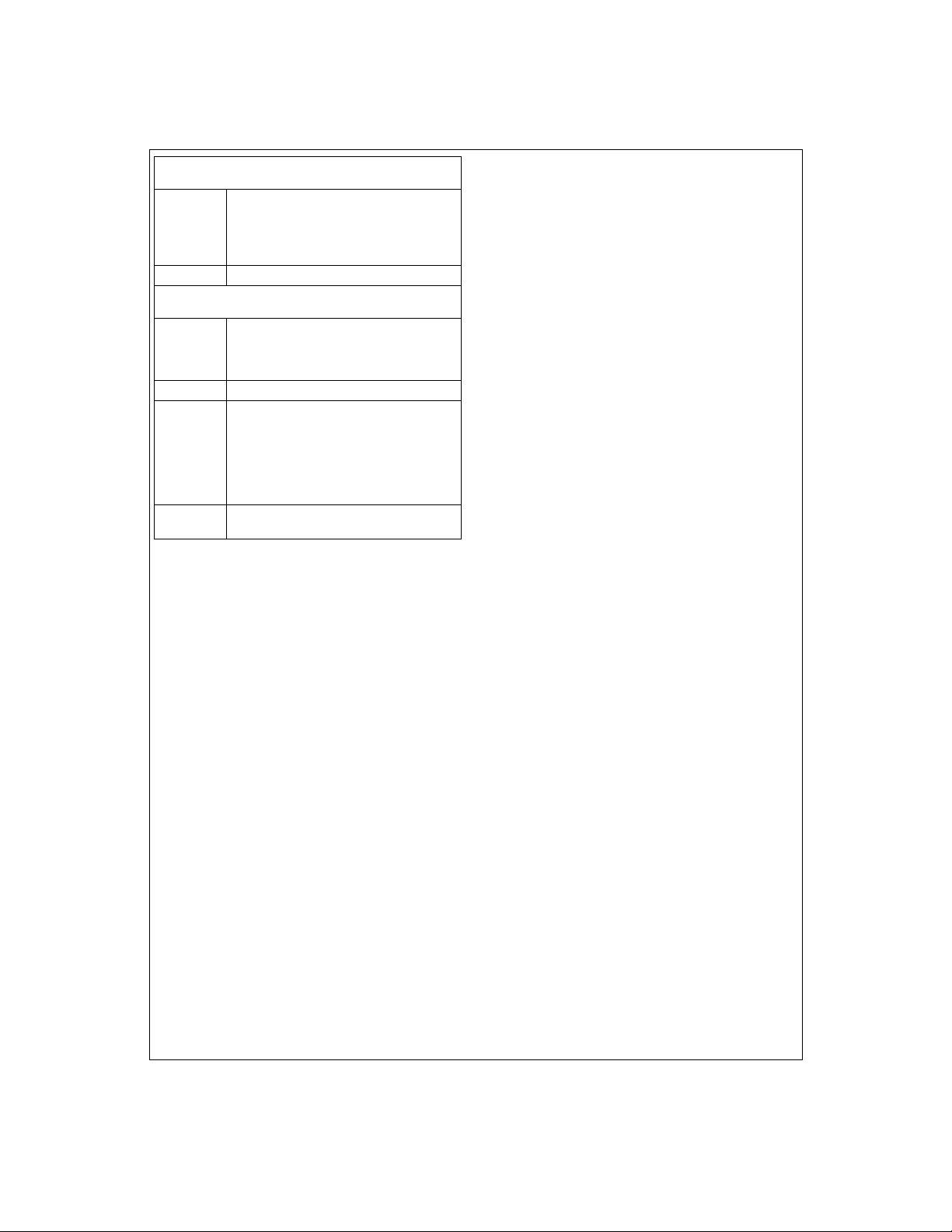
Page 20

Address
(Decimal)
Address
(Binary)
A4 A3 A2 A1 A0 D7 D6 D5 D4 D3 D2 D1 D0
21 10101
22 10110
23 10111
24 11000
25 11001
26 11010
27 11011
28 11100
Data Bits
Reset Pulse Width Reset Pulse Position
Bit 2 Bit 0 Bit 4 Bit 0
Reference Sample Position
- - - Bit 4 Bit 0
Signal Sample Position
- - - Bit 4 Bit 0
Misc Group 2
Signal
Polarity
Coefficient
Preview 1 Preview 2
8 or 10 bit
Power
Coefficient
Down
Gain
Write
Phase
TB7TB6000000
00000000
Bus
Offset
Coefficient
Write
Phase
Data Read
Phase
Internal/
External
- TR2 Enable TR1 Enable RS Enable Ø2 Enable Ø1 Enable
Ø1 Polarity
During TR1
SYNC
pulse
Misc Group 3
Misc Group 4
Test Mode 1
Test Mode 2
TR Pulse
Mode
(1 or 2
Pulses)
TR2 Pulse
Polarity
Red/Blue
Order for
2 Output
sensors
TR1 Pulse
Polarity
3 or 2
Output
sensor
RS Pulse
Polarity
Standard
or
Odd/Even
sensor
Ø1/Ø2
Polarity
Table 2: Configuration Register Parameters
t
Note:
MCLK
Parameter
(Address)
Red
Offset DAC (0)
Green
Offset DAC (1)
Blue
Offset DAC (2)
= 1/f
= 1 MCLK period. Examples given in parenthesis are for f
MCLK
Control Bits Result
D5
(SIGN)
0
0
0
• • •
0
0
1
1
1
• • •
1
1
D4
D3
D2
(MSB)
• • •
• • •
0
0
0
0
0
0
• • •
1
1
0
0
0
1
1
0
0
0
• • •
1
1
1
1
0
0
0
• • •
1
1
0
0
0
• • •
1
1
D1
• • •
• • •
20
= 24MHz (t
MCLK
D0
(LSB)
0
0
1
0
1
0
• • •
1
1
0
0
1
0
1
0
1
0
• • •
1
1
0
1
= 41.66ns).
MCLK
Typical Offset
(in ADC LSBs)
0.00
+4.2
+8.4
• • •
+126.0
+130.2
0.00
-4.2
-8.4
• • •
-126.0
-130.2
http://www.national.com
Page 21

Table 2: Configuration Register Parameters
t
Note:
MCLK
= 1/f
= 1 MCLK period. Examples given in parenthesis are for f
MCLK
(Continued)
MCLK
= 24MHz (t
= 41.66ns).
MCLK
Parameter
(Address)
Red PGA
(3)
Green PGA
(4)
Blue PGA
(5)
Coarse Color
Balance PGA
(Blue with x3
multiplier bit set)
(5)
Internal
Offset
Subtractor
Coefficient
(6)
D7
0
0
0
• • •
0
0
0
D7
1
1
1
• • •
1
1
1
D7
(MSB)
0
0
0
• • •
1
1
1
Control Bits Result
D4
(MSB)
0
0
0
• • •
1
1
1
D4
(MSB)
0
0
0
• • •
1
1
1
D6
0
0
0
• • •
1
1
1
D5
• • •
D4
0
0
0
1
1
1
0
0
0
• • •
1
1
1
D3
0
0
0
• • •
1
1
1
D3
0
0
0
• • •
1
1
1
D3
0
0
0
• • •
1
1
1
D2
• • •
D2
• • •
D2
• • •
D1
0
0
0
1
1
1
0
0
0
1
1
1
0
0
0
1
1
1
0
0
1
• • •
0
1
1
D1
0
0
1
• • •
0
1
1
D1
0
0
1
• • •
0
1
1
D0
(LSB)
0
1
0
• • •
1
0
1
D0
(LSB)
0
1
0
• • •
1
0
1
D0
(LSB)
0
1
0
• • •
1
0
1
Typical Gain
(V/V)
0.93
1.00
• • •
3.00
Typical Gain
(V/V)
2.79
3.00
• • •
9.00
Offset
(in ADC LSBs)
0
1
2
• • •
253
254
255
Internal
Multiplier
Gain
Coefficient
(7, 8)
Internal/External
Coefficient
Clocks (9)
Number of
Coefficient
Clocks (9)
Number of
Databuses in
System (9)
D9
(MSB)
0
0
0
• • •
1
1
1
D7
0
1
D5
0
1
D4
0
1
D8
• • •
D7
0
0
0
1
1
1
0
0
0
• • •
1
1
1
• • •
• • •
• • •
• • •
21
D2
• • •
D1
0
0
0
1
1
1
0
0
1
• • •
0
1
1
D0
(LSB)
0
1
0
• • •
1
0
1
External Coefficien t Clock Source
Internal Coefficient Clock Source
GCLK and OCLK
GCLK only
2 Databuses
1 Databus
Gain
(V/V)
See
Equation 5
http://www.national.com
Page 22

Table 2: Configuration Register Parameters
t
Note:
MCLK
= 1/f
= 1 MCLK period. Examples given in parenthesis are for f
MCLK
(Continued)
MCLK
= 24MHz (t
= 41.66ns).
MCLK
Parameter
(Address)
Multiplier Gain
Range
(9)
Multiplier
Coefficient
Source
(9)
Offset Coefficient
Source
(9)
Dummy Pixels
(Minimum Value
is 0)
(10)
Optical Black
Pixels
(Minimum Value
is 1)
(11)
D3
D1
D0
D7
• • •
D7
• • •
Control Bits Result
0
0
1
1
0
1
0
1
0
0
0
1
1
1
0
0
0
1
1
1
D2
D6
• • •
D6
• • •
0
1
0
1
0
0
0
1
1
1
0
0
0
1
1
1
D5
0
0
0
• • •
1
1
1
D5
0
0
0
• • •
1
1
1
D4
0
0
0
• • •
1
1
1
D4
0
0
0
• • •
1
1
1
D3
• • •
D3
• • •
0
0
0
1
1
1
0
0
0
1
1
1
D2
0
0
0
• • •
1
1
1
D2
0
0
0
• • •
1
1
1
Range 0, 67% (1:3)
Range 1, 50% (1:2)
Range 2, 33% (1:1.5)
External CD0-CD9 Bus
Internal Register
External CD0-CD9 Bus
Internal Register
D1
0
0
1
• • •
0
1
1
D1
0
1
1
• • •
0
1
1
D0
0
1
0
• • •
1
0
1
D0
1
0
1
• • •
1
0
1
Not Used
0
1
2
• • •
253
254
255
1
2
3
• • •
253
254
255
Active Pixels
(Minimum Value
is 0)
(12, 13)
End of Line
Integration Pixels
(Minimum Value
is 5)
(14, 15)
D13
(MSB)
0
0
0
• • •
1
1
1
D13
(MSB)
0
0
0
• • •
1
1
1
D12
• • •
D12
• • •
D11
0
0
0
1
1
1
0
0
0
1
1
1
0
0
0
• • •
1
1
1
D11
0
0
0
• • •
1
1
1
• • •
• • •
• • •
• • •
• • •
• • •
• • •
• • •
22
D2
• • •
D2
• • •
D1
0
0
0
1
1
1
1
1
1
1
1
1
0
0
1
• • •
0
1
1
D1
0
1
1
• • •
0
1
1
D0
(LSB)
0
1
0
• • •
1
0
1
D0
(LSB)
1
0
1
• • •
1
0
1
Active Pixels
0
1
2
• • •
16381
16382
16383
End-of-Line Pixe ls
5
6
7
• • •
16381
16382
16383
http://www.national.com
Page 23

Table 2: Configuration Register Parameters
t
Note:
MCLK
= 1/f
= 1 MCLK period. Examples given in parenthesis are for f
MCLK
(Continued)
MCLK
= 24MHz (t
= 41.66ns).
MCLK
Parameter
(Address)
TR1
Pulse Duration
(16)
TR2
Pulse Duration
(17)
TR1/TR2 - Ø1
Guardband
(18)
Optical Black
Clamp Start
Position
(Must be Š
RS Pulse Width)
(19)
D
5
(MSB)
0
0
0
• • •
1
1
1
D
5
(MSB)
0
0
0
• • •
1
1
1
4
D
(MSB)
0
0
0
• • •
1
1
1
D4
• • •
D4
• • •
D3
• • •
Control Bits Result
D3
0
0
0
0
0
0
• • •
1
1
1
1
1
1
D3
0
0
0
0
0
0
• • •
1
1
1
1
1
1
D2
0
0
0
0
0
0
• • •
1
1
1
1
1
1
D2
0
0
0
• • •
1
1
1
D2
0
0
0
• • •
1
1
1
D1
0
0
1
• • •
0
1
1
D1
0
0
1
• • •
0
1
1
D1
0
0
1
• • •
0
1
1
D0
(LSB)
0
1
0
• • •
1
0
1
D0
(LSB)
0
1
0
• • •
1
0
1
D0
(LSB)
0
1
0
• • •
1
0
1
= (x/2)t
t
pixel
3 channel mode,
t
pixel
, where
pixel
= 12t
MCLK
= 8t
MCLK
channel mode
for
for 2
(except for x = 0:
duration for x = 0 is
0.5tpixel, same as
for x = 1)
= (x/2)t
t
pixel
3 channel mode,
t
pixel
, where
pixel
= 12t
MCLK
= 8t
MCLK
channel mode
for
for 2
(except for x = 0:
guardband for x = 0
is 0.5tpixel, same
as for x = 1)
TR Pulse Width
0.5 t
pixel
0.5 t
pixel
1.0 t
pixel
• • •
30.5 t
pixel
31.0 t
pixel
31.5 t
pixel
TR Guardband
0.5 t
pixel
0.5 t
pixel
1.0 t
pixel
• • •
30.5 t
pixel
31.0 t
pixel
31.5 t
pixel
Clamp Start
(1/(2*f
MCLK
0
))
1
2
• • •
29
30
31
Optical Black
Clamp Stop
Position
(20)
Reset Pulse
Width
(Minimum Value
Is 1)
(21)
D4
(MSB)
0
0
0
• • •
1
1
1
7
D
(MSB)
0
0
0
1
1
1
1
D3
• • •
D6
D2
0
0
0
0
0
0
• • •
1
1
1
1
1
1
D5
(LSB)
0
1
1
0
0
1
1
1
0
1
0
1
0
1
D1
0
0
1
• • •
0
1
1
23
D0
(LSB)
0
1
0
• • •
1
0
1
Clamp Stop
(1/(2*f
MCLK
0
))
1
2
• • •
29
30
31
RS Pulse Width
(1/(2*f
MCLK
1
))
2
3
4
5
6
7
http://www.national.com
Page 24

Table 2: Configuration Register Parameters
t
Note:
MCLK
= 1/f
= 1 MCLK period. Examples given in parenthesis are for f
MCLK
(Continued)
MCLK
= 24MHz (t
= 41.66ns).
MCLK
Parameter
(Address)
Reset Pulse
Position
(21)
Reference
Sample
Position
(22)
Signal
Sample
Position
(23)
D
4
(MSB)
0
0
0
• • •
1
1
1
D
4
(MSB)
0
0
0
• • •
1
1
1
D4
(MSB)
0
0
0
• • •
1
1
1
D3
• • •
D3
• • •
D3
• • •
Control Bits Result
D2
0
0
0
0
0
0
• • •
1
1
1
1
1
1
D2
0
0
0
0
0
0
• • •
1
1
1
1
1
1
D2
0
0
0
0
0
0
• • •
1
1
1
1
1
1
D1
0
0
1
• • •
0
1
1
D1
0
0
1
• • •
0
1
1
D1
0
0
1
• • •
0
1
1
D0
(LSB)
0
1
0
• • •
1
0
1
D0
(LSB)
0
1
0
• • •
1
0
1
D0
(LSB)
0
1
0
• • •
1
0
1
Reset Position
(1/(2*f
MCLK
0
))
1
2
• • •
29
30
31
Reference Position
(1/(2*f
MCLK
0
))
1
2
• • •
29
30
31
Signal Position
(1/(2*f
MCLK
0
))
1
2
• • •
29
30
31
Signal Polarity
(24)
Preview Mode
(24)
SYNC Pulse
(24)
TR Pulses
(24)
Red/Blue Order
for GRGB CCDs
(24)
Sensor Type
(24)
D7
D6
D4
D3
D2
D1
0
1
Negative, CDS On (CCD)
Positive, CDS Off (CIS)
D5
0
0
1
1
0
1
0
1
0
1
0
1
0
1
0
1
Normal Operation
Normal Operation
2x Speed
4x Speed
Externally Supplied (SYNC is Input)
Internally Generated (SYNC is Output)
1 TR Pulse (TR1)
2 TR Pulses (TR1 and TR2)
GR First
GB First
Dual Output (RG-BG)
Triple Output (R-G-B)
24
http://www.national.com
Page 25

Table 2: Configuration Register Parameters
t
Note:
MCLK
= 1/f
= 1 MCLK period. Examples given in parenthesis are for f
MCLK
(Continued)
MCLK
= 24MHz (t
= 41.66ns).
MCLK
Parameter
(Address)
Sensor Type
(24)
Power Down
(25)
Coefficient Bus
Width
(25)
TR2 Enabl e
(25)
TR1 Enabl e
(25)
RS Enable
(25)
Ø2 Enable
(25)
Ø1 Enable
(25)
D0
D7
D6
D4
D3
D2
D1
D0
Control Bits Result
0
1
0
1
0
1
0
1
0
1
0
1
0
1
0
1
In 8 bit mode, coefficient data is 8 bits wide,
input through CD0-CD7.
Standard
Even/Odd
Operating
Low Power Standby Mode
10 bit
8 bit
TR2 Enabled
TR2 Disabled
TR1 Enabled
TR1 Disabled
RS Enabled
RS Disabled
Ø2 Enabled
Ø2 Disabled
Ø1 Enabled
Ø1 Disabled
Gain Coefficient
Write Phase
(26)
Offset Coefficient
Write Phase
(26)
Data Read Phase
(26)
Ø1 Polarity
During TR1
(26)
TR2 Pulse
Polarity
(26)
TR1 Pulse
Polarity
(26)
D7
D6
D5
D4
D3
D2
0
1
0
1
0
1
0
1
0
1
0
1
25
0°
180°
0°
180°
0°
180°
High
Low
High
Low
High
Low
http://www.national.com
Page 26

Table 2: Configuration Register Parameters
t
Note:
MCLK
= 1/f
= 1 MCLK period. Examples given in parenthesis are for f
MCLK
(Continued)
MCLK
= 24MHz (t
= 41.66ns).
MCLK
Parameter
(Address)
RS Pulse Polarity
(26)
Ø1/Ø2 Polarity
(26)
Test Mode
(27)
Test Mode
(28)
Control Bits Result
D1
0
1
D0
0
1
TB7
TB6
0
0
1
0 0 0 0 0 0 0 0 Set all bits to 0
0
1
1
Set bits D0-D5 to 0
Test Output Is CDS Signal
Test Output is Clamp Signal
High
Low
Ø1 High/Ø2 Low
Ø1 Low/ Ø2 High
Test Output Low
26
http://www.national.com
Page 27

Applications Information
1.0 THEORY OF OPERATION
The LM9812 removes error s from and digitizes up t o 3 channe ls
of linear sensor pixel stream s, while providing all the necessar y
clock signals to drive the sensor. Offset and gain errors are
removed at the pixel rate, for individual pixels. Offset errors are
removed through corr elated double sampling (CDS), an analog
offset DAC for large DC offsets, and finally a pixel-rate digital offset subtractor for individual pixel offsets. Gain erro rs (which may
come from any combination of PRNU, uneven illumination, cos
effect, RGB filter mismatch, etc.) are re moved through th e use of
a 5 bit PGA in front of t he A DC ( for coarse ga i n cor re ction ) an d a
10x10bit pixel-rate digital multiplier for individual pixel gain errors.
1.1 ANALOG SIGNAL PATH (See Functional Block Diagram)
1.1.1 Clamping and Buffering
The Output Signals ( OS) fro m the ima ge sensor are capac itively
coupled to the three (OS
LM9812. Inside the LM9812, a DC restore operation is performed
by clamping the input signal to 2.5V when the input signal is
known to be black (during t he star t of a new line of image da ta).
To eliminate loading of the input signal, the signal is buffered
through a source follower before being sent to the CDS section.
1.1.2 CDS
The LM9812 uses a high performance C DS (Correlated Do uble
Sampling) circuit to remove many sources of noise and error from
the CCD signal. It also support s CIS image sensors with a single
sampling mode for positive-going signals.
Figure 1 shows the output stage of a typ ical CCD and the resulting output waveform:
RS (RESET)
(from shift register)
Ø1
RS
OS
Capacitor C1 converts the electrons coming from the CCD’s shift
register to an analo g voltage. The source follower output stage
(Q2) buffers this voltage be fore it leaves the CCD. Q1 resets the
voltage across capacitor C1 in between every pixel at intervals 2
and 5. When Q1 is on, th e out put si gnal (OS) i s at its most p ositive voltage. After Q1 turns off (period 3), the OS level represents
the residual voltage across C1 ( V
charge injection f rom Q1, therma l noise from the ON resistance
of Q1, and other sources of error. When the shift register clock
, OSG, OSB) analog inputs of the
R
V
DD
Q1
C1
e-
Q2
OS
V
SS
123 4 5
Figure 1: CDS
). V
RESIDUAL
RESIDUAL
includes
(Ø1) makes a low to h i gh tran sition (period 4), the electrons from
the next pixel flow into C1. The charge across C1 now contains
the voltage propor tional to the number of electron s plus V
, an error term. If OS is sampled at the end of period 3 and
UAL
that voltage is subtracted from t he OS at the e nd of per i od 4, the
V
reduced ([V
principal of Correlated Double Sampling.
term is canceled and the noise on the signal is
RESIDUAL
SIGNAL+VRESIDUAL
]-V
RESIDUAL
= V
SIGNAL
). This is the
The LM9812’s CDS circuit acquires a signal within a 1 M C LK w in dow which can be placed anywhere in the pixel period with 0.5
4
MCLK precision. Se e Diagram 12 for more de tailed timing in formation.
1.2 CIS Mode
The LM9812 provides some support for CIS (Contact Image Sensor) devices by offering a sampling mode for capturing positive
going signals, as opposed to the CCD’s negative going signal.
The output signal of a CIS sensor ( Figure 2) dif fers from a CCD
signal in two primar y ways: its output increases with incr easing
signal strength, and it does no t usually have a reference level as
an integral part of the output waveform of every pixel.
OS (CIS)
OS (CCD)
123 4 5
Figure 2: CIS vs. CCD Output signals
When the LM9812 is in CIS mode (Re gister 24, bit 7 =1), it uses
the V
pixel. Since the LM9812 cla mps the input signal to V
level as the reference (or black) voltage for each
REF MID
the black portion at the beginning of every line, the output of the
sampler is an accurate and repea table repre sentation of t he that
pixel’s brightness.
1.2.1 Static PGAs
The output of the CD S stage drives the PGAs (Programmable
Gain Amplifiers). E ach PGA provide s 5 bits of fixed gain correction over a 0.93V/V to 3V/V (-0.6 to 9.5dB) range. The Blue channel has an optional x3 stage for a gain range of 2.8 V/V to 9.0 V/V
(8.9 to 19d B). Th e ga in o f ea ch P G A s h oul d be se t duri ng c al i br ation to bring the maximum amplitude of the strongest pixel to a
level just below the desired maximum outpu t from the ADC. The
gain is determined by the following equation:
Gain
V
--- -
V
0.93
PGA code
------------------- --------2.137+=
32
Equation 1: PGA Gain
The Blue Channel has an additional gain stage w ith a gain of
3V/V that may be switched on to compensate for the low amplitude blue output of some sensors. With the x3 bit set (Register 2,
bit 7=1), the blue gain is:
Gain
V
--- -
V
02.79
PGA code
-------------------- -------6.411+=
32
Equation 2: Blue Channel PGA Gain with x3 Bit Set
RESID-
REF MID
at
27
http://www.national.com
Page 28

This PGA is static - it does not change at the pixel rate. The PixelRate Shading Multiplier is used to eliminate pixel-to-pixel gain
errors (typically sensor PRNU and shading errors).
1.2.2 Static Offset DACs
The Static Offset DACs remove DC offsets generated by the sensor and the LM98 12’s analog signal chain. T he DACs should be
set during calibration to the lowest value that still resu lts in an
ADC output code > 0 for all the pixels. Each LSB of the offset
DAC is typically 4.2 ADC LSBs, providing a total offset adjustment range of ±130 ADC LSBs. The equation for the offset DAC
is:
()
Offset ADC LSBs
Equation 3: Offset DAC
Like the PGA, the Offse t DAC is static - it do es n ot change at the
pixel rate. The Pixel Rate Offset Subtrac tor is used to eliminate
pixel-to-pixel offset errors.
1.2.3 ADC
The 10 bit ADC quantizes the out put from the analog chai n and
passes the result to the digital section for pixel rate error correction. The ADC’s input range is equal to V
gain constant compensat ing for all sources of gain error throu ghout the entire analog signal path.
1.3 DIGITAL SIGNAL PATH
1.3.1 Pixel-Rate Offset Subtractor
The output of the ADC is fed to the Pixel-Rate Of fset Subtractor.
Each pixel of image data may have a different offset error. If bit 0
of Register 9 is set to a 0 a nd a byte rep re sent ing the offset error
code is fed to the Pixel-Rate Offset Subtractor through the CD0CD9 databus, the offset for each pixel can be subtracted from the
ADC output code at the pixel conversion rate. If this feature is not
desired, the Offset Su btrac tor can be set to a fixed value by wr iting the desired value to Regist er 6 and se tting bit 0 of Regi ster 9
to a 1.
Offset Subtractor Out ADC Output Offset Error Code
The offset subtractor input is 8 bits wide, input on CD0-CD7, for a
correction range of 0 to 255. Informat ion on bits CD 8 and CD9 i s
ignored.
1.3.2 Pixel-Rate Shading Multiplier
The Pixel Rate Shading Multiplier follows the Offset Subtractor.
This stage compensa tes for nonuniformities between individual
pixels (shading error). Each pixel of image data may have a different gain error. If bit 1 of Register 9 is set to a 0 and a word representing the gain correction coefficient is fed to the Pixel-Rate
Shading Multiplier through the CD0-CD9 databus, the gain for
each pixel is changed at the pixel rate to eliminate pixel-to- pixel
gain errors. If this feature is not desired, the Shading Multiplier
can be set to a fixed value by writing the desired gain value to
Registers 7 and 8 and setting bit 1 of Register 9 to a 1.
The equation for calc ulating the ga in of the multipli er is given in
Equation 5. The Pixel Rate Shading Mul tiplier ha s three different
gain ranges as shown i n
the strongest pixel to the weakest pixel is less than 1.5, the multi-
Equation 4: Offset Subtractor
Tabl e 1
4.2 DAC Code
=
()
/C, where C is the
REF IN
=
–
. For systems where the ratio of
Multiplier Gain(V/V) 1
Equation 5: Shading Multiplier Gain
plier gain range setting of 1:1.5 provides very accurate contro l of
the gain of each pixel. Systems with la rge r variat i on ca n use gain
ranges of 1:2 or 1:3.
Multiplier Gain Range
Minimum Gain
(V/V, Multiplier Input = 0)
Maximum Gain
(V/V, Multiplier Input = 1024)
N (used in Equation 5) 2048 1024 512
Bits D3, D2 of Register 9 1, 0 0, 1 0,0
Table 1:Shading Multiplier: 10 bit Coefficient Bus Width
When the 8 bit Coef fici en t Bus W id th is s elect ed ( R eg ister 25 , bi t
6=1), the coefficient da ta is only 8 bits wide, supplied on CD0CD7. This reduces the accuracy of the gain correction, but allows
the use of an 8 bit path to store coefficient data, instead of a 10 or
16 bit wide path.
Multiplier Gain Range
Minimum Gain
(V/V, Multiplier Input = 0)
Maximum Gain
(V/V, Multiplier Input = 256)
N (used in Equation 5) 512 256 128
Bits D3, D2 of Register 9 1, 0 0, 1 0,0
Table 2:Shading Multiplier: 8 bit Coefficient Bus Width
1.4 SENSOR CLOCK GENERATION
The LM9812 generates all of the clock signals required to directly
drive most commercial linear CCDs and some CIS - no external
clock buffers are necessary. Most linear CCDs designed for scanner applications require 0 to 5V signal swings into 20 to 500pF
input loading. Series r esistors are typically inser ted between the
driver and the CCD to control slew rate and isolate the driver from
the large load capacitances. The values of these resistors are
given in the CCD’s datasheet.
1.4.1 TR1 and TR2
The LM9812 supports one or two TR ( transfer, or shift) pulses as
shown in Diagrams 8 and 9. This pulse is used to transfer the
contents of each pixel’s photodiode to the CCD’s serial shift register for clocking out of the CCD. Configuration Re gisters 16, 17,
and 18 control th e TR1, TR2, and T R guardband pulse widths,
while Register 24, b it 3 determines whe ther the LM9812 gene rates TR1 only or bo th TR1 and TR2 at the begi nning of a line.
The polaritie s of the TR pulses are determined by Registe r 26,
bits 2 and 3. If not ne eded, one or both TR p ulses can be disabled by setting Register 25, bits 3 and 4 to the appropriate value.
28
Gain Correction Coefficient
----------------- --------------------------------- --------------------- -+=
N
1:1.5
1:2.0
(50%)
1:2.0
(50%)
1:3.0
(67%)
1:3.0
(67%)
(33%)
111
1.5 2.0 3.0
1:1.5
(33%)
111
1.5 2.0 3.0
http://www.national.com
Page 29

1.4.2 RS
The LM9812 also generates the RS (reset) pulse required to
clear the CCD’s output capacitor of the previous pixel’s charge.
The RS pulse’s width and position (relative to the edge of the ø1
pulse) is determ ined by the value in Configuration Register 21.
See Diagrams 10 and 12. The p olarity of the RS pul se is determined by Register 26, bit 1. If n ot needed, thi s pulse can be disabled by setting Register 25, bit 2 to a 1.
1.4.3 ø1 and ø2
ø1 and ø2 are the two phase clock for the CCD shift register. ø2
is always the inverse of ø1. For “standard” CCDs, the ø1 and ø2
frequency is equal to th e pixel rate, the same frequency as the
RS pulse. In Standard Mode, the RS pulse position and Sample
Reference/Sample Signal edges are set with respect to the falling
edge of ø1. For “even/odd” CCDs, the ø1 and ø2 frequency is
equal to one half the pixel rate, a pixels is sampled after both the
rising and falling edges of the ø clock. In Even/Odd Mode, the RS
pulse position and Sample Reference /Sample Signal edges are
set with respect to the either ed ge of ø1. Stand ard or Even/Odd
mode is selected by se tting bit 0 of Register 24. The absolute
polarity of the ø pulses is determined by Register 26, bits 0 and 4
(both bits perfor m the s ame f unc tion). If not need ed, one or b oth
ø pulses can be disabled by setting Register 25, bits 0 and 1 to
the appropriate value.
1.5 DIGITAL INTERFACE
There are three main sections to the digital interface of the
LM9812: the Configu ration Register interface (through w hich all
device programming is done), the Correction Coefficient Data
interface (the 10 bit-wide input databus for gain and offset correction coefficients), an d the 10 bit-wide Pixel Data ou tput databus
(where the corrected digital output data appears).
1.5.1 Configuration Register I/O
The Configuration Re gister is written to and read from thro ugh
the D0-D9 databus, using the CS
, WR, and RD signals. To write
to the Configuration Register, follow the timing shown in Diagram
24. The first byte is the address of the Configuration Register to
be written to, the second byte is the data to be stored at that
address. Configuration Register writes can occur at any time,
independent of the state of the SYNC pin.
To read from the Configurati on Registe r, follow the timing shown
in Diagram 25. The fi rst byte is the a ddress of the Configuration
Register to be written to, the second byte is the data stored at that
address. The SYNC pin must be low in order to rea d from the
Configuration Register. To ensure that SYNC is low when in the
SYNC out mode, RUN/STOP
must be low until the end o f the
active pi xels.
If the LM9812’s RD
pin is taken low,
D0-D9 databus will be driven. Never take the RD
even if the CS pin is high
pin low unless
, the
you are actually doing a Configuration Register read.
1.5.2 Pixel Data I/O
The output of the multi plier is available on the D0-D9 d atabus. If
the Data Read Pha se bit (b it 5 of Registe r 26) is set to a 0, Data
changes shortly before the falling edge of EOC
for t
changes shor t ly be fore the r i sing ed ge of EO C
. If the Data Read Phase bit is set to a 1, Data
DATAVALID
and remains valid
and remains valid
for t
SYNC is high and RD PIXEL
. The D0-D9 databus comes out of tri-state when
DATAVA LI D
is low. If SYNC is low, RD PIXEL will
have no effect.
When reading pixel data, RD PIXEL
may be driven by EOC, putting the data on the bus only when EOC is low, and allowing other
data on the bus (such as CD0-CD9 correction data) at other
times. In this way the output data and correction co efficient data
can share the same databus (See Diagrams 16, 17, 20, and 21).
1.5.3 Correction Coefficient Data I/O
Coefficient data for the pixel rate Offset Subtract or and Shading
Multiplier enters t he LM9812 thro ugh the CD0-CD9 da tabus. To
maximize flexibility for the system designer, there are several
clocking options available in this mode: separate or combined
buses for the CD0-CD9 and the D 0-D9 dat a, one (GL CK) or two
(GLCK and OCLK) clock signals to latch the Correction Coefficient data, and the option to have the LM9812 generate the clock
signals or have them suppli ed to the LM9812. Timing for these
different options is shown in Diagrams 14 through 21, and
described below.
CD0-CD9
separate from
D0-D9
(2 bus)
GLCK, OCLK are
outputs (2 Clock)
GLCK is output
(1 Clock)
GLCK, OCLK are
inputs
CD0-CD9 tied to
D0-D9
(1 bus)
Diagram 16 Diagram 14
Diagram 17 Diagram 15
Diagrams 20, 21 Diagrams 18, 19
Table 3:Correction Databus Options
Diagram 14 shows the case where the correction data (CD0CD9) is on a separate bus from the output data (D0-D9) (Register
9, bit 4=0). The GLCK and OCL K signals are generated by the
LM9812 (Register 9, bit 5=0, bit 7=1). Gain correction data is
latched on the rising edge of GCLK, and offset correction data is
latched on the rising edge of OCLK. There is a one EOC
clock
latency between the latching of the gain coefficient for a particular
pixel and the output of that pixel on the D0-D9 databus.
Diagram 15 shows the case where the correction data (CD0CD9) is on a separate bus from the output data (D0-D9) (Register
9, bit 4=0). The LM98 12 gene rates the GCL K signal only (R egister 9, bit 5=1, bi t 7=1) . Gain correc tion data is lat ched o n the ri sing edge of GCLK, and o ffset correction data is latched on the
falling edge of GCLK. There is a one EOC
clock latency between
the latching of the gain coefficient for a particular pixel and the
output of that pixel on the D0-D9 databus.
Diagram 16 shows the case where the correction data (CD0CD9) is on the s ame bus a s th e out put da ta (D 0 -D9) ( Regist er 9,
bit 4=1). The GLCK and OCLK signals are generated by the
LM9812 (Register 9, bit 5=0, bit 7=1). Gain correction data is
latched on the rising edge of GCLK, and offset correction data is
latched on the ris ing edge of OCLK. Using the EOC
control the RD PIXEL
input allows the CD0-CD9 and the D0-D9
output to
data to exist on the same bus with no contention. There is a one
29
http://www.national.com
Page 30

EOC clock latency between the latching of the gain coefficient for
a particular pi xel and the output of that pixel on the D0-D9 da tabus.
Diagram 17 shows the case where the correction data (CD0CD9) is on the sam e bus as the ou tpu t d ata (D 0 -D9 ) ( Reg i ster 9,
bit 4=1). The LM9812 ge nerates the GCLK signal only (Reg ister
9, bit 5=1, bit 7=1). Gain cor rection data is latched on the rising
edge of GCLK, and offset correction d ata is lat ched on th e falling
edge of GCLK. Using th e EOC
output to control the RD PIXEL
input allows the CD0-CD9 and the D0-D9 data to exist on the
same bus with no conten tion. There is a one EOC
clock latency
between the latching of the gain coefficient for a particula r pixel
and the output of that pixel on t he D0-D9 databus.
In the previous modes of operation, the offset correction clock
(OCLK) and the gai n (sh ading) correct ion cl ock (GCLK) ar e generated by the LM9812 and used to generate the RD
pulses to
coefficient RAM. These clocks can also be configured a s inputs
to allow compatibility with some existing ASICs or designs where
it is preferred to let the ASIC ge nerate all the timing. The o ffset
data is always latched on the rising edge of OCLK. The gain data
is always latched on the rising edge of GCLK.
To operate the LM9812 with an externally supplied OCLK and
GCLK, set bit D7 of register 9 to a 0 and set the phase bit for
each clock. The procedure to determine the state of the phase bit
is described at the end of this section.
DIagrams 18 through 21 show the timing required when GCLK
and OCLK are configured as inputs to the LM9812 (Register 9, bit
5=0, bit 7=0). This op tion exists to al low the LM9812 to work wi th
ASICs designed for earlier systems, where the ASIC ge nerates
the SRAM timing (instead of the LM9812). Diagrams 18 and 19
show the 2 bus mode (Re gister 9, bi t 4=0), diagrams 20 and 21
show the 1 bus mode (Register 9, bit 4=1).
In these modes, G LCK a nd O CLK com e fro m an exter n al sour ce
that may be asynchronous to th e int er nally ge nerated OCLK a nd
GCLK. While these clocks may be asynchronous, they will be the
same frequency, the ADC conversion rate (since offset and gain
coefficients are nee ded for every pixel, a nd the pi xel data rate is
fixed by the ADC conversion rate).
The circuit shown in Figure 3 is implemented insi de the LM9812
to synchronize (by delaying) the external coefficient clock s and
CD0-9 data with the interna l LM981 2 clo cks.
Q
DQ
FF2
DQ
FF1
O
Ext OCLK
CD0-9
DQ
FF1
G
Q
Ext GCLK
EOC
Figure 3: Using An External OCLK and GCLK
CD0-9 data is always latched into register FF1 on the rising edge
of the external clock. The output of FF1 is then latched by FF2 on
the
falling
edge of the external clock. So the latched data is available at the output of FF1 between the rising edges of the external
clock, and is valid at the output of FF2 between the falling edges
of the external clock. If the phase difference between the external
Internal OLCK
phase = 0°
phase = 180°
O
Q
DQ
FF2
G
Q
clock and EO C
3:1
Mux
DQ
FF3
O
Q
Internal GLCK
phase = 0°
phase = 180°
3:1
Mux
DQ
FF3
(the LM9812’s internal coefficient clock) is known,
G
Q
Latched
Offset
Correction
Data to
Offset Sub-
tractor
Latched
Correction
Multiplier
then by selecting Q1 or Q2 as the i nput to FF3 , the desig ner can
guarantee that the data will be valid on the rising edge of
GCLK
, where it is latched into FF3 and synchronized to the
INT
LM9812.
GCLK
is not externally available to the user but it is basically
INT
30
http://www.national.com
Gain
Data to
Page 31

the inverse of EOC, plus or minus a few ns of gate delay. To use
an external GLCK and OC LK, determ ine the phase of the external OCLK and GLCK with respect to EOC
. Then look at Diagrams
18 and 19 (2 bus mode) or 20 and 21 (1 bus mode). Choose a
phase setting (0° or 180 °, registe r 26 bits 6 an d 7) for OCLK and
GCLK that provides the most margin with r espect to the t
EOC
1 (OCLK IN)
specifications.
, t
OCLK-EOC2 (OCLK IN)
, and t
GCLK-EOC (GCLK IN)
OCLK-
It is entirely possible that either setting (0° or 180°) will work
equally well. The condition th at must be avoided is when FF3 is
clocked (falling edge of EOC) at the same time the input data to
FF3 is changing (ri sing edge of OCLK/GCLK for 0° p has e, or falling edge of OCLK/GCLK for 180° phase). As long as this does
not occur simultaneously, the data will be correctly latched.
Note that the coeffici ent da ta must ap pear so oner ( relative to the
pixel output data) for the C lock I n mod es, to acco unt for the extra
latency through FF 1 and FF2. This additional time is shown in
Diagrams 18 through 21.
This mode of ope ratio n m ay seem confusing at first, but it i s n ecessary to allow the synch ronous LM9812 to ph ase lock to external coefficient data of unknown phase.
1.5.4 MCLK
This is the master clo ck input for the LM9812. Th e ADC conversion rate is fixed at 1/4 of this frequency. The pixel rate in 3 channel mode is 1/12 of the MCLK frequency. Many of the timing
parameters are also relative to the frequency of this clock.
1.5.5 SYNC
This input signals the beginning of a line. When SYNC goes high,
the LM9812 genera tes a TR pulse, then b egi ns conver ting pixels
until the SYNC line is brought low again. If SYNC is externally
applied, the LM9812 will work with sensors with any number of
pixels. If SYNC is internally generated (in combina tion with the
RUN/STOP
input), sensors with up to 3 cha nnels of 16383 pix-
els/channel can be used.
1.5.6 RUN/STOP
The LM9812 has a “SYNC OUT” mode (Register 24, bit 4=1) that
automatically generates a SYNC pulse stream based on the number of active pixels a nd the numbe r of ad ditional end -of-li ne in tegration pixels programmed into registers 12-15. When the
RUN/STOP
the periodic SYNC pulse. When RUN/STOP
pin is brought high, the LM 9812 begins generating
goes low, the
LM9812 will continue converting the remaining active pixels, then
SYNC will go low and the par t will “idle” u ntil the next rising e dge
of RUN/STOP
.
Using the SYNC OUT mode provides a simple way to clock the
sensor continuously with a repeatable, user-programmed integration period. By varying th e number of e nd-of-line integration pixels (in registers 14 and 15) , the integration time (and thus the
amplitude of the out put signal from t he sensor) can be adjusted
with very high accuracy ( about 1 part in 5400, or 0.02%, for a
600dpi sensor).
CCD sensors (this mode will not work for CIS se nsors). In these
modes, adjacent pixels are averaged together in the analog
domain and converted at the maximum ADC conversion rate.
This allows the CCD data to be clo cked out and digitized 2 or 4
times faster (corresponding to a 2 to 4 times faster image scan ).
The image will be 1/2 or 1/4 the resolution. For example, a 600dpi
sensor will look like a 300dpi sensor in th e x2 preview mode, or a
150dpi sensor in th e x4 preview mode. Thi s is useful because it
allows faster scans for lower resolution images and scan preview
images. The quality of t he lower resolution image i s also significantly improved because this technique
averages
pixels to
reduce the resolu tion instead of discarding pixels (which oft en
results in a loss of image information).
Ø1
(Even/Odd Mode)
Ø2
(Even/Odd Mode)
Ø1
(Standard Mode)
Ø2
(Standard Mode)
3
1.5 1.5 3 66
All lengths given in units of MCLK periods
9
RS
OS
CDS
(Internal)
p
n
p
n+1
Hold Ref Hold Signal
Diagram 4: x2 Preview Mode Timing
In the x2 preview mode, the Ø clock is clocked at 2 times the normal Ø clock frequency, while the RS pulse stays at the ADC’s
conversion rate. By skipping every other RS pulse, the charge for
pixel n+1 will be added to the charge for pixel n on the CCD itself.
Since the CCD is being clocked at 2 times the normal rate, the
period between lines (and therefore the integration time) w ill be
half as long, causing t he amplitude of each pixel to be half as
large. Since the output of the CCD is the sum of two pixels, the
final amplitude seen by the LM 9812 is ver y sim ilar to w hat it is in
normal mode. The final pixel amplitude will be equal to (p
p
/2) = (pn + p
n+1
)/2 = the average of pn and p
n+1
n+1
.
n
/2 +
The same principle applies in the x4 preview mode. Here the Ø
clock is clocked at 4 times the normal Ø clock frequency, while
the RS pulse stays at the ADC’s conversion rate. By skipping 3
out of 4 RS pulses, the charge for pixels n, n+1, n+2, and n+3 will
be averaged in the CCD’s output stage. Since the CCD is being
clocked at 4 times the norma l rate, the pe r iod betwee n l ine s (a nd
therefore the integration time) will be one quarter as long. The
final pixel amplitude will be equal to (p
the av erage of p
, p
, p
n+1
n+2
, and p
n
n+3
+ p
+ p
+ p
n
n+1
.
n+2
n+3
)/4 =
Getting the optimum p erformance out of the preview modes with
a particular CCD may require adjusting the RS pulse width, RS
pulse position, Sample Reference, and Sample Signal timing
(Registers 21, 22, and 23).
2.0 PREVIEW MODE OPERATION
The LM9812 suppor ts two “p review” or low resolutio n modes for
31
http://www.national.com
Page 32

Ø1
(Even/Odd Mode)
Ø2
(Even/Odd Mode)
Ø1
(Standard Mode)
Ø2
(Standard Mode)
7.5
6
1.5 1.5 7.5
1.5
0.5
111.5
1
All lengths given in units of MCLK periods
6
RS
p
Hold Ref
n
p
n+1
p
n+2
p
n+3
Hold Signal
OS
CDS
(Internal)
Diagram 5: x4 Preview Mode Timing
3.0 ANALOG INTERFACE
3.1 Voltage Reference
The V
age. The LM4041-ADJ adjustable bandgap reference is recom-
pin should be connected to a 2V±5% reference volt-
REF IN
mended for this application, as shown in Figure 6. The
inexpensive “D” grade meets all t he requir ements of the appl ication and is available in a TO-92 (LM4041 DIZ-ADJ) package as
well as a SOT-23 package (LM4041DIM3-ADJ) to minimize board
space. To reduce noise, the V
pin should be bypassed to
REF IN
Reference
Amplifiers
V
V
A
10.5k
10.1k
R
REF HI OUT
V
REF HI IN
0.1µF
V
REF MID OUT
V
REF MID IN
0.1µF
V
REF LO OUT
V
I=V
REF IN
-I +I
/2R
R
V
REF IN
REF LO IN
0.1µF
0.1µF
V
A
3k
4.7k
LM9812
LM4041-ADJ
3k
Figure 6: Voltage Reference Generation
AGND with a 0.1µF monolithic capacitor.
The LM9812 genera tes three internal reference voltages for its
analog front end: V
equal to 0.49*V
, or 2.45V with a nominal 5V supply. V
A
REF MID
, V
REF HI
, and V
REF LO
. V
REF MID
REF IN
drives a transconductanc e amplifier with two output curre nts, V
/2 and +V
REF IN
V
reference voltage buffers, which generate a nominal
REF LO
3.45V (V
REF HI
V
- V
REF MID
sense (IN) inputs are broug ht out to the chip for bypassing. Each
REF IN
/2. These currents go into the V
REF IN
= V
+ V
REF MID
/2). To minimize noise, the reference amplifiers
/2), and 1.45V (V
REF IN
buff er ’s output and input s h oul d be t ied t o ge the r an d de c ou pl ed t o
AGND through a 0.1µF monolithic capacitor.
3.2 Clamp Capacitor Selection
This section is very long because it is relatively complicated to
explain, but the answer is short and simple : A clamp capacitor
value of 0.01µF should work in almost all applications. The rest of
this section describes exactly how this value is selected.
C
CLAMP
OS
OS
SENSOR
DOS
NC
2.450V
LM9812
Figure 7: OS Clamp Capacitor and Internal Clamp
The output signa l of many se nsors r ides on a DC of fset (great er
than 5V for many CCDs) which is incompatible with the LM9812’s
5V operation. To eliminate this offset without resorting to ad ditional higher voltage comp onents, the outp ut of the sen sor is AC
coupled to the LM 981 2 t hro ug h a D C blocking ca pacit or, C
(the CCD’s DOS output, if available, is not used). The value of
this capacitor is determined by the leakage current of the
LM9812’s OS input and the output impedance of the sensor. The
leakage through the OS input determines how quickly the capacitor value will drift from the clamp value of V
determines how ma ny pixels can be pr ocessed be fore the droop
REF MID
causes errors in the conversion (±0.1V is the recommended
limit). The output impedance of the sensor determines how
quickly the capacitor can be char ged to the clamp value during
the black reference period at the beginning of every line.
The minimum clamp capacitor value is determined by the maximum droop the LM9812 can tolerate while converting one sensor
line. The following equation takes the maximum leakage curre nt
into the OS input, the maximum allowable droop (100mV), the
number of pixels on the sensor, and the pixel conversion rate
(f
/12 for triple output sensors or f
MCLK
sors) and provides the minimum clamp capacitor value:
C
CLAMP MIN
i
-------- -dt=
dV
leakage current (A)
-------------------- ------------------------------ -
Equation 6: C
max droop(V)
CLAMP MIN
/8 for dual output se n-
MCLK
number of pixels
-------------------- --------------------------------- -=
conversion rate (Hz)
Calculation
For example, if the OS input leakage curren t is 20nA worst -case,
the sensor has 2700 active pixels, the conversion rate i s 2MHz
(f
= 24MHz, triple output sensor), and the max droop desired
MCLK
is 0.1V , the minimum clamp capacitor value is:
20nA
2700
------------- -
-------------- -=
0.1V
2MHz
Example
http://www.national.com
is
32
C
CLAMP MIN
Equation 7: C
270pF=
CLAMP MIN
and
REF HI
REF LO
CLAMP
, which then
=
Page 33

The maximum size of the clamp capacitor i s determined by the
amount of time available to cha rge it to the de sired value during
the optical black por tion of th e senso r outp ut. Th e in ter nal cla mp
is on for each pixel for the time specified in Registers 19 and 20
(see Diagram 11). This time can be calcul ated using this equation:
(s)
Start-Stop
-----------------------------------=
2 f
DARK
MCLK
(Hz)
Calculation
t
DARK
Equation 8: t
Where Start is the Optical Black Clam p Start Position (Register
19), Stop is the Optical Black Clam p Sto p Position (Registe r 20),
f
is the MCLK frequency, and t
MCLK
(per pixel) that the clamp is on.
is the amount of time
DARK
The following equation ta kes the number of optical bla ck pixels,
the amount of time (per pixel) that the clamp is closed, the sensor’s output impedance, and the desired accuracy of the final
clamp voltage and provides the maxi mum clamp capacitor value
that allows the cla mp capacitor to settle to the des ired accuracy
within a single line:
t
C
CLAMP MAX
Equation 9: C
Where n = the number of optical black pixels, t
of time (per pixel) that the cla mp is o n, R
ance of the CCD, and accuracy is the rat io of the worst- case ini-
----- -
------------------ --------------=
R
ln(accuracy)
n
----------------- R
OUT
CLAMP MAX
1
t
(s)
DARK
-------------------- ------------=
ln(accuracy)
Calculation
DARK
is the output imped-
OUT
is the amount
tial capacitor voltage to the desired final capac itor voltage. For
example, if a sensor has 18 black reference pixels, the output
impedance of the sensor is 15 00Ω, the LM9812 is configured to
clamp for 375ns, the worst case in itial voltage a cross th e capaci tor is 10V, and the desired voltage after clamping is 0.1V (accuracy = 10/0.1 = 100), then:
18
C
CLAMP MAX
Equation 10: C
The final value for C
C
CLAMP MAX
work in this example.
, but no less than C
CLAMP MAX
should be less than or equal to
CLAMP
------------ 1500
977pF=
CLAMP MIN
375ns
----------------- -=
ln(100)
Example
. A value of 470pF will
In some cases, depending primarily on the choice of sensor,
C
CLAMP MAX
the capacitor can n ot be charged to its final voltage during the
may actually be
less
than C
CLAMP MIN
, meaning that
black pixels at the beginning of a line and hold it’s voltage without
drooping for the duration of that line. This is usually not a problem
because in most ap plications the sensor is clo cked continuously
as soon as power is applied. In this case, a la rger capacitor can
be used (guarantee ing that the C
and the final clamp voltage is forced across the capacitor over
CLAMP MIN
requirement is m et),
multiple lines. This equation calculates how many lines are
required before the capacitor settles to the desired accuracy:
R
C
OUT
lines
Equation 11: Line Settling Formula
CLAMP
---------------- -
------------------ -------
n
t
DARK
Initial Voltage
ln=
------------------- ------------------
Final Voltage
Using the values shown before an d a clamp capacitor value of
0.01µF, this works out to be:
1500
0.01µF
lines
------------ -
----------------- -
18
375ns
Equation 12: Line Settling Example
10V
----------- -
0.1V
10.2 lines=ln=
At a 2MHz conversion rate, this is about 14ms.
In this example a 0.01µF capaci tor t akes 14ms a fter p ower-up to
charge to its final value, but its droop across all subseq uent lines
is now less than 3mV (using the previous example’s values). This
wide margin is the reason a C
most applications.
value of 0.01µF will work in
CLAMP
4.0 CALIBRATION
System calibration is required to correct the many sources of
error in a scanner and optimize image quality. There are many different ways to calibrate a system, some take a long time but produce better results, othe rs a re faster w it h po ten tiall y lower qu al ity
images. The method d escribed below should pr oduce ver y good
results, but it is by no means the only way to approach sca nner
calibration. Some ca libration steps could be eli minated to speed
up the calibration procedure. Other steps could be impr oved by
iteratively repeating the m, verifying that th e previous calculation
achieved the desired result. Every scanner system is different, so
every system may benefit from optimization of the calibration routine.
4.0.1 LM9812 Configuration Sequence After Powe r-On
The power-on reset circuit of the LM 9812 may take several hundred microseconds. Wait 1ms after power-on before writing to the
Configuration Registers.
Make sure the SYNC and RUN/STOP
inputs are low before writing to the Confi guration Reg isters. When SYNC is high, you can
not read the configuration register (but you can still write to it).
The LM9812 configuration sequence:
• Set bit 2 of Test Register 28 to 0 (to allow writing of
configuration data). This register is reset to 0 by the power-on
reset, but this step is still recommend ed to ensure that wr ites
will work even if this register was corrupted.
• Program bit 4 of re gi ste r 2 4 t o d ete rmine if the LM 981 2 will be
used in the SYNC OUT or SYNC IN mode.
• Cycle the Powerdown bit to reset the LM9812’s state
machines. (Take bit 7 of register 25 to a 1, then back to a 0).
This procedure will completely reset the part. At this time the
LM9812 is ready for data to be written to all 28 configuration registers. Data can also be read back from all 28 register s if write
confirmation is desired.
After all 28 configuration r egi st ers h ave been program me d, sca nning can begin by taking SYNC high (in the SYNC IN mode) or
RUN/STOP high (in the SYNC OUT mode).
4.1 Calibration Initialization
• Set the Offset DACs to their maximum positive value (Offset
DAC registers 0, 1, and 2 =31)
• Set the PGA gains to 1V/V (PGA gain registers 3, 4, and 5 =1)
• Set the Pixel Rate Offset A dder Sou rce to inter nal (reg ister 9,
bit 0=1)
• Set the Pixel Rate Multiplier Source to internal (register 9, bit
1=1)
• Set the Inter nal Pixel Rate Offset Adder value to 0 (register
6=0)
• Set the Internal Pixel Rate Multiplier value for a gain of 1
(registers 7 and 8 = 0)
33
http://www.national.com
Page 34

• Set the Multip lier Gai n Range to 1: 3 (regist er 9, bi ts 2 and 3 =
00)
4.2 Setting the Static Offset DACs
018
Black
MIN
ADC
Output
Code
014
010
00C
008
004
000
Data Pixels
Figure 8: Finding Black
MIN
• Scan one line of a pure black test pattern, or scan one line with
the light source turned off. (Caution: turning the light source on
and off may cause thermal drift in light intensity as the light
source warms up and cools down.) Scanning multiple black
lines and averaging each pixel from each line will reduce noise
and increase the accuracy of this step.
• Find the minimum pixel value of the scanned black image
(Black
) for each color (Figure 8).
MIN
• Reduce the Offset DAC value for each color so that the
minimum black pixel is close to 0, but still greater than 0
(Figure 9). One offset DAC code = ~4.2 ADC LSBs, so change
the DAC code to (31 - Black
018
014
010
ADC
Output
00C
Code
008
004
000
Data Pixels
MIN
/4.2).
Black
Black
Black
MIN
too high
MIN
correct
MIN
too low
= 13:
= 6:
= 0:
Figure 9: Setting the Static Offset DACs
• Because the above equation is based on typical LM9812
performance, the new DAC settings should b e verified. Scan
another black line(s) with the new DAC values and verify that
all the pixels are still above 0. If any pixels are equal to 0,
increment the DAC value by 1. If the minimum pixel is above 8,
consider decrement ing the DAC value by 1. Repeat this step
until the minimum pixel value of the scanned black image
(Black
) for each color is greater than 0 but less than 9.
MIN
Black
values greater than 9 are acceptable (they will be
MIN
removed by the Pixel Rate Offset Subtractor), but will reduce
the dynamic range of the system.
4.3 Setting the Static PGAs
• Decide on the Target Code for your scanner. This is the
maximum output code from the ADC for a pure white image.
This code may be as large as 1023, but this value could cause
clipping if the light sourc e drifts and becomes brighter after
calibration. A value of 1000 allows for moderate light source
drift between calibration and image scan.
• Scan one line of a pure white test pattern. Scan ning multiple
white lines and averaging each pixel from each line will reduce
noise and increase the accuracy of this step.
• Find the maximum white pixel value of the image data
(White
• Program the PGA value for each color so that the ma ximum
) for each color (Figure 10).
MAX
white pixel is close to, but still less than the Target Code
(Figure 11). The PGA gain required to m eet this condition is
equal to the Target Code divided by White
. Using the PGA
MAX
Target Code
White
MAX
ADC
Output
Code
Data Pixels
Figure 10: Finding White
MAX
gain too high
Target Code
gain correct
gain too low
ADC
Output
Code
Data Pixels
Figure 11: CCD Input Signal In Range
gain equation (Equation 1), the PGA code required is:
PGA code Integer
=
Target Code
------------------- ------------- -0.94
White
MAX
–
32
-------------- -
2.137
Equation 13: PGA Code Calculation
If the Blue channel requires a gain greater than 3 (Target
Code/White
Equation 14:
PGA code Integer
is >3), then set regi ster 2, bit 7=1 and use
MAX
Target Code
=
------------------- ------------- -2.82
White
MAX
–
32
-------------- -
6.411
Equation 14: Blue PGA Code Calculation, x3 Bit Set
• Program the calculated PGA values for each color into
configuration registers 3, 4, and 5.
• Because the above equatio ns are based on typical LM9812
performance, the new PGA settings sho uld be verified. Scan
another white line(s) with the new PGA values and recalculate
White
and White
MAX
white image) for each color. Verify th at White
still below the Target Code. If White
equal to the target code, decrement that PGA value by 1.
(the minim u m AD C out pu t c ode for the
MIN
MAX
is near but
MAX
is greater than or
•
4.4 Determining the Multiplier Correction Range Setting
• For best performance, repeat Steps 4.2 and 4.3 before
proceeding. This will maximize the available dynamic range of
the ADC and ensure that all the pixels are in range.
• Digitize another white line (or multiple lines) and calculate the
minimum and maxi mum pixels from that line (White
White
). Verify that White
MAX
Target Code
ADC
Output
Code
is less than the Target Code.
MAX
White
White
MAX
MIN
Data Pixels
Figure 12: Determining Correction Range Setting
• The correction range required (Range) = White
• If Range < 1.5, th en set the Multiplier Ran ge bits (register 9,
MAX
/White
bits 3 and 2) to 10 (33%).
34
http://www.national.com
MIN
and
MIN
Page 35

• If 1.5 < Range < 2.0, then set the Multiplier Range bits (register
9, bits 3 and 2) to 01 (50%).
• If 2.0 < Range < 3.0, then set the Multiplier Range bits (register
9, bits 3 and 2) to 00 (66%).
• If Range > 3.0 , then s et the ra nge is too la rge an d the sys tem
can not be calibrated.
4.5 Calculating the Pixel Rate Offset Coefficients
• Scan one line of a pure black test pattern, or scan one line with
the light source turned off. (Caution: turning the light source on
and off may cause thermal drift in light intensity as the light
source warms up and cools down.) Scanning multiple black
lines and averaging each pixel from each line will reduce noise
and increase the accuracy of this step.
• The value of each pixel is the o ffset error for that pixel. Store
each pixel value into that pixel's offset correction RAM
location.
• Set the Pixel Rate Offset Ad der Sour ce to extern al (regist er 9,
bit 0 = 0)
4.6 Calculating the Pixel Rate Multiplier Coefficients
• Scan one line of a pure white test pattern. Scan ning multiple
white lines and averaging each pixel from each line will reduce
noise and increase the accuracy of this step.
• The equation for the multiplier gain is:
Multiplier Gain 1
x
--- -+=
N
Equation 15: Multiplier Gain Equation
where:
x is the 10 bit multiplier gain coefficient (0 to 1023),
N = 2048 (Multiplier range = 1:1.5),
N = 1024 (Multiplier range = 1:2),
N = 512 (Multiplier range = 1:3).
• Determi ne the multiplier gai n for each pixel n so the result is
the Target Code:
Gain(n)
Target Code
------------------ -------------- -=
pixel data
n
Equation 16: Gain Calculation for Each Pixel
• The multiplier coefficient required is therefore:
Multiplier Coefficent (n) Integer(N(Gain(n) - 1))=
Target Code
Integer N
------------------ -------------- -1
pixel data
=
–
n
Equation 17: Multiplier Coefficient Calculation for Each Pixel
• Store the Multiplier Gain Coefficients for each pixel into that
pixel's offset correction RAM location.
• Set the Pixel Rate Multiplier Source to external (register 9 , bit
1=0)
CALIBRATION COMPLETE
4.7 Additional Calibration Information
The procedure detail ed in se ctions 4.1 throug h 4.6 i s only on e of
many approaches to scanner calibration. I n some approach es it
may be useful to use a model for the analog front en d and a ctually measure V
OS1
and V
OS2
.
Figure 13 is a mathematical model of the analog front end of one
channel of the LM9812. The constant C (typically 2, given in the
Electrical Characteristics table) represents the total gain error
from Vin through D
To further simplify the model, the signal is always assumed to be
with G = 1V/V (PGA register setting = 1).
OUT
0V for black and increasing in the positive direction as pixel
brightness increases. In reality, black may be offset from ground,
and white may be negative (CCD) or positive (CIS) with respect to
black, but this is all taken care of by the CDS function and the correct setting of the Signal Polarity bit (Register 24, bit 7).
V
REF IN
C
+
V
IN
G
Σ
+
V
OS1
+
+
Σ
Σ
+
+
V
OS2
Offset
DAC
10 Bit
ADC
V
OD
D
OUT
Figure 13: Simplified Model of One Channel of the Ana-
log Front End
The analog front end’s transfer function is shown in Equation 18.
D
OUT
VINV
()
+
1024
C
OS
------------------- --------------------------------------- ----------------------------- -=
GV
++
1
V
REFIN
OS
V
OD
2
Equation 18: AFE Transfer Equation
The typical values of C (2) and V
out. It is also useful to convert all the voltag es to ADC codes,
(2V) cancel each other
REFIN
since that is the domain in which they will be seen by the calibration software. V
can be more easily accomplishe d using the simplified model of
(in ADC codes) = VIN (in V)*1024. Calibra tion
IN
Equation 19.
D
()
OUTVINVOS
GV
+
++=
1
OS
V
OD
2
Equation 19: AFE Transfer Equation (units of ADC LSBs)
Measurement of th e two o ffset volta ge s ( V
by measuring the AD C output , with a black image on th e sensor
OS1
and V
OS2
) is done
(if a black reference image is not available, it may be created simply by turning off the scanner’s illumination). In this example, V
is considered to be 0V, and any offsets from the sensor are
lumped in with the LM9812’s V
with a PGA gain of 1V/V and 3V/V, then the offset errors (V
and V
) can be determined from the following two equations:
OS2
V
= 1V
= 3V
OS1
OS1
OS1
and V
V
V
OS1
OS2
+ V
+ V
OS2
= (3V
ADC1
V
ADC2
Solving for V
. If the ADC output is measured
OS1
(PGA gain = 1V/V)
+ V
+ V
DAC2
DAC2
(PGA gain = 3V/V)
OS2
OS2
:
= (V
- V
- V
ADC1
ADC2
)/2
)/2
ADC2
ADC1
OS1
5.0 POWER SUPPLY CONSIDERATIONS
5.1 General
The LM9812 should be powered by a single +5V source (unless
5.2
3V-compatible digital I/O is required-see Section
supplies (V
out individually to allow separate bypassing for e ach supply input.
They should
) and the digital suppl ies (VD and V
A
not
be powered by two or more different supplies.
). The analog
) are brought
DI/O
IN
35
http://www.national.com
Page 36

In systems with separate analog and dig ital +5V supplies, all the
supply pins of the LM9812 shou l d be powere d by the analog +5 V
supply. Each supply input should be bypassed to it s respective
ground with a 0.1µF cap acito r l oc ate d as clo s e a s pos si ble to the
supply input pin. A single 10µF tantalum capacitor should be
placed near the V
ing.
supply pin to provide low fr equency bypass-
A
To minimize noise, keep the LM9812 an d all analog compon ents
as far as possible from noise generators, such as switching power
supplies and high freque ncy digita l busses. If po ssible, isolate a ll
the analog compo nents and signals (OS, reference inputs and
outputs, V
the digital ground plane. The two ground pla nes should be tied
, AGND) on an analog groun d plane, separate from
A
together at a single poin t, preferably the point where the power
supply enters the PCB.
5.2 3V Compatible Digital I/O
If 3V digital I/O operatio n is desired, the V
ered by a separate 3V±10% or 3.3 V±10% su pply. In this case all
pin may be pow-
DI/O
the digital I/O pins (CD0-CD9, D0- D 9, MCL K, SYNC, RUN/STOP
CS
, RD, WR, EOC, GLCK, OCLK, and RD PIXELI) will be 3V
compatible. The CCD clock signals (Ø1, Ø2, RS, TR1 and TR2)
remain 5V outputs, p owered by V
should be bypassed to DGND
0.1µF capacitor and a 10µF tantalum capacitor.
. In this case, the V
D
with a parallel combination of a
I/O
DI/O
input
5.3 Power Down Mode
Setting the Power Down bit to a “1” puts the device in a low power
standby mode. The CCD outputs (Ø1, Ø2, RS, TR1 and TR2) are
pulled low and the analog sections are turned o ff to conserve
power. The digital logic will continue to operate if MCLK continues
and SYNC is held high, so for minimum power dissipa tion MCLK
should be stopped when the LM9812 enters the Power Down
mode. Recovery from Power Down typically takes 50µs (the time
required for the reference voltages to settle to 0.5 LSB accuracy).
6.0 RULES, HINTS, AND COMMON DESIGN PROBLEMS
6.1 Ignore MCLK When Designing a System
While the MCLK inp ut is the master clock for all the LM 9812 timing, it should not be used to predi ct when other clocks or events
will occur. To get the highest possible timing resolution, the
LM9812 uses double-e dged flip flops for many functions. CCD
clock output signals, coefficient clocks, and intern al clocks may
change state on the rising or falling edge of MCLK, depending on
the state of MCLK and some internal free running state machines
when the RUN/STOP
or SYNC input goe s high. Norm al proces s
variations from par t to par t result in different delays between an
MCLK edge and other events in the LM9812.
For a reliable design, synchronize your system to EOC
, GCLK,
and OCLK. These si gnals are repeat able from device to device.
Do not synchronize your system to MCLK: treat it on ly as a frequency that sets the pixel rate o f the sys tem. If you need t o generate additional CCD timing signals, synchronize them to the
LM9812’s TR and RS outputs.
STATE D. If the voltage on the input pi n is at the thr eshold, large
amounts of current can be drawn from the digital I/O supply
because the N and the P channel of the input buffer are simultaneously on. These latches are very weak (sourcing and sinking
about 50µA typically) and can be easily overdriven.
From
Multiplier
From
Config
10
D0-D9
Register
To
Config
Register
,
6.3 Don’t Decrement the Reference Sample Position Register by 1
Figure 14: Weak Latches On Databus
A write to the Reference Sampl e Position Register ( C onf igura ti on
Register 22) contain ing a value that is 1 less than the current
value stored in the Reference Sample Position Register will
sometimes make one of the L M981 2’s internal s tate ma chines to
fail, causing erratic and improp er operation of the LM9812. For
example, if the value current ly stored in the Reference Sam ple
Position Register is 12, then writing an 11 can cause this problem.
To avoid this condition, never decrement the existing value stored
in the Reference Sample Position Register by 1. Increm enting by
any amount or decreme nting by 2 or greater or writ ing the sam e
number over again will not cause any problems.
To get out of this mode, write a new number to the Reference
Sample Position Register that is greater than the original number.
Since incrementing and decrementing this register should only be
done during the development phase of the s ystem until an ideal
value for this register is cho sen. This issue sho uld cause absolutely no problems in production, since the value of this regist er
will be fixed, so the firmware should never write more than the
final ideal value to this register.
6.4 Taking RD
In many digital systems, the RD
Low With CS High Will Drive the Databus
signal is ignored when CS is held
high. This is not the c ase with the The LM9812 . Taking RD
with CS
high will take the D0-D9 databus out o f tristate and put
random data on the d atabus. Do not assu me that RD
when CS
is high.
low
is ignored
6.2 Weak Latches On Databus
The D0-D9 databus has weak latches on its output pins to keep
the databus from dr ifting throu gh the input ’s trip point when T RI-
36
http://www.national.com
Page 37

Physical Dimensions
inches (millimeters)
52-Pin Plastic Leaded Chip Carrier (PLCC)
Order Number LM9812CCV
NS Package Number V52A
LIFE SUPPORT POLICY
NATIONAL'S PRODUCTS ARE NOT AUTHORIZED FOR USE AS CRITICAL COMPONENTS IN LIFE SUPPORT
DEVICES OR SYSTEMS WITHOUT THE EXPRESS WRITTEN APPROVAL OF THE PRESIDENT OF NATIONAL
SEMICONDUCTOR CORPORATION. As used herein:
1. Life support devices or systems are devices or systems which,
(a) are intended for surgical im plant into the body, or (b) support
or sustain life, and whose failure to perfor m, when prop erl y used
in accordance with instructions for use provided in the labeling,
can be reasonably expected to result in a sign ifican t injury to the
user.
N
National Semicond uc tor
Corporation
1111 West Bardin Road
Arlington, TX 76017
Tel: 1(800) 272-9959
Fax: 1(800) 737-7018
http://www.national.com
National does not assume any responsibility for use of any circuitry described, no circuit patent licenses are implied and National reserves the right at any time without notice to change said circuitry and specifications.
National Semicond uc tor Europe
Fax: a49 (0) 180-530 85 86
Email: europe.support @ nsc.com
Deutsch Tel: + 49 (0) 180-530 85 85
English Tel: + 49 (0) 180-532 78 32
Francais Te l: + 49 (0) 180-532 93 58
Italiano Tel: + 49 (0) 180-534 16 80
2. A critical comp one nt is any co mpo ne nt o f a l ife support device
or system whose failure to perform can be reasonably expected
to cause the failure of the life suppor t device or system, or to
affect its safety or effectiveness.
37
National Semiconductor Hong
Kong
13th Floor, Straight Block,
Ocean Centre, 5 Canton Rd.
Tsimshatsui, Kowloon
Hong Kong
Tel: (852) 2737-1600
Fax: (852) 2736-9960
National Semicondu c tor
Ltd. Japan Ltd.
Tel: 81-043-299-2308
Fax: 81-043-299-2408
http://www.national.com
 Loading...