

Page 1
LM9811
10-Bit Greyscale/30-Bit Color
Linear CCD Sensor Processor
LM9811 10-Bit Greyscale/30-Bit Color Linear CCD Sensor Processor
April 1998
General Description
The LM9811 is a high performance integrated signal
processor/digitizer for linear CCD image scanners. The
LM9811 performs all the analog processing (correlated
double sampling for black level and offset compensation,
pixel-by-pixel gain (shading) correction, and 10-bit
analog-to-digital conversion) necessary to maximize the performance of a wide range of linear CCD sensors.
The LM9811 can be digitally programmed to work with a
wide variety of CCDs from different manufacturers. An internal configuration register sets CCD and sampling timing to
maximize performance, simplifying the design and manufacturing processes.
The LM9811 can be used with parallel output color CCDs. A
signal inversion mode eases use with CIS sensors. For
complementary voltage reference see the LM4041.
Applications
n Color and Greyscale Flatbed and Sheetfed Scanners
n Fax and Multifunction Peripherals
n Digital Copiers
n General Purpose Linear CCD Imaging
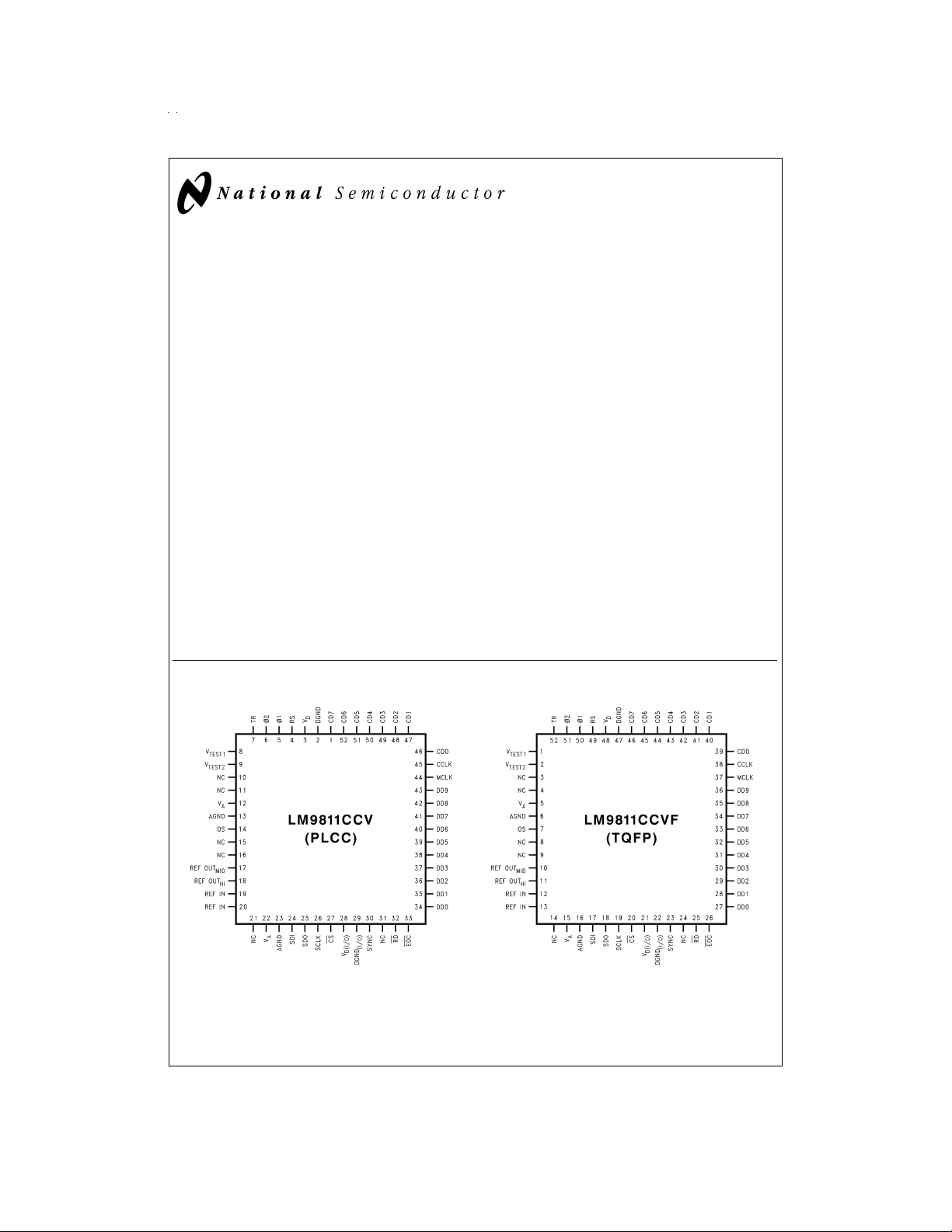
Connection Diagrams
Features
n 1.5 Million pixels/s conversion rate
n Pixel-rate shading correction for individual pixels
maximizes dynamic range and resolution, even on
“weak” pixels
n Implements Correlated Double Sampling for minimum
noise and offset error
n Reference and signal sampling points digitally controlled
in 40ns increments for maximum performance
n Generates all necessary CCD clock signals
n Compatible with a wide range of linear CCDs
n Supports some Contact Image Sensors (CIS)
n TTL/CMOS input/output compatible
Key Specifications
n Resolution: 10 Bits
n Pixel Conversion Rate: 1.5MHz
n Supply Voltage: +5V
n Supply Voltage
(Digital I/O): +3.3V
n Power Dissipation: 260mW (max)
±
10%or +5V±5
±
5
%
%
DS012813-1 DS012813-2
TRI-STATE®is a registeredtrademark of National Semiconductor Corporation.
™
MICROWIRE
SPI
© 1999 National Semiconductor Corporation DS012813 www.national.com
is a trademark of National Semiconductor Corporation.
™
is a trademark of Motorola, Inc.
Page 2
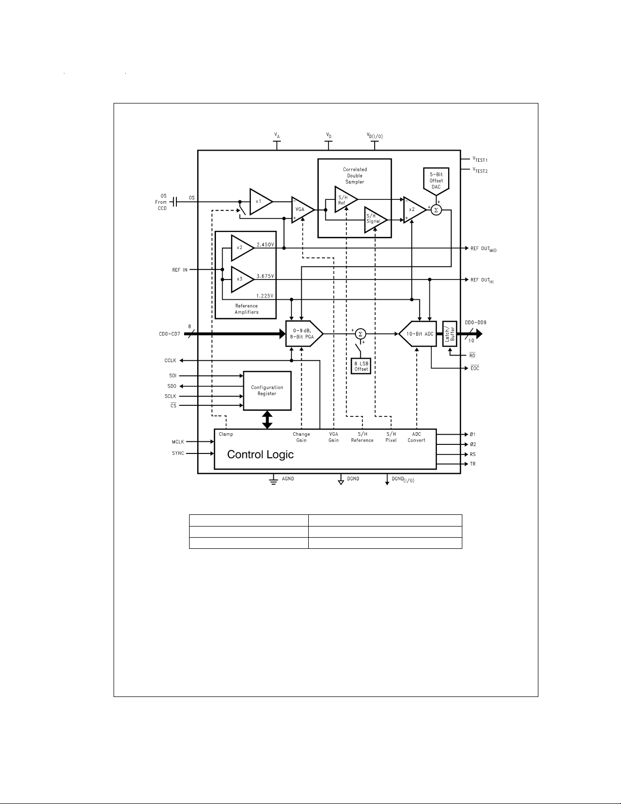
Block Diagram
Ordering Information
Commercial (0˚C ≤ TA≤ +70˚C) Package
LM9811CCV V52A 52-Pin Plastic Leaded Chip Carrier
LM9811CCVF VEG52A 52-Pin Thin Quad Flatpack
www.national.com 2
DS012813-3
Page 3
Absolute Maximum Ratings (Notes 1, 2)
+
=
=
=
Positive Supply Voltage (V
V
V
A
D
with Respect to
GND=AGND=DGND=DGND
(I/O)
Voltage on any Input or Output Pin 0.3V to V
Input Current at any Pin (Note 3)
Package Input Current (Note 3)
=
Package Dissipation at T
25˚C (Note 4)
A
ESD Susceptibility (Note 5)
Human Body Model 2000V
Soldering Information (Note 6)
Infrared, 10 seconds
LM9811CCV 300˚C
)
V
D(I/O
6.5V
+
+0.3V
±
25 mA
±
50 mA
Operating Ratings (Notes 1, 2)
Operating Temperature
Range T
LM9811CCV, LM9811CCVF 0˚C ≤ TA≤ +70˚C
Supply Voltage +4.75V to +5.25V
V
A
Supply Voltage +4.75V to +5.25V
V
D
Supply Voltage +2.7V to +5.25V
V
D(I/O)
| ≤ 100 mV
|V
A–VD
V
A–VD(I/O)
OS, REF IN Voltage Range −0.05V to V
CD0–CD7, MCLK, SYNC,
SDI, SCLK, CS, RD,
Voltage Range −0.05V to V
MIN
D(I/O)
≤ TA≤ T
≥ −100 mV
+ 0.05V
A
+ 0.05V
LM9811CCVF 220˚C
Storage Temperature −65˚C to +150˚C
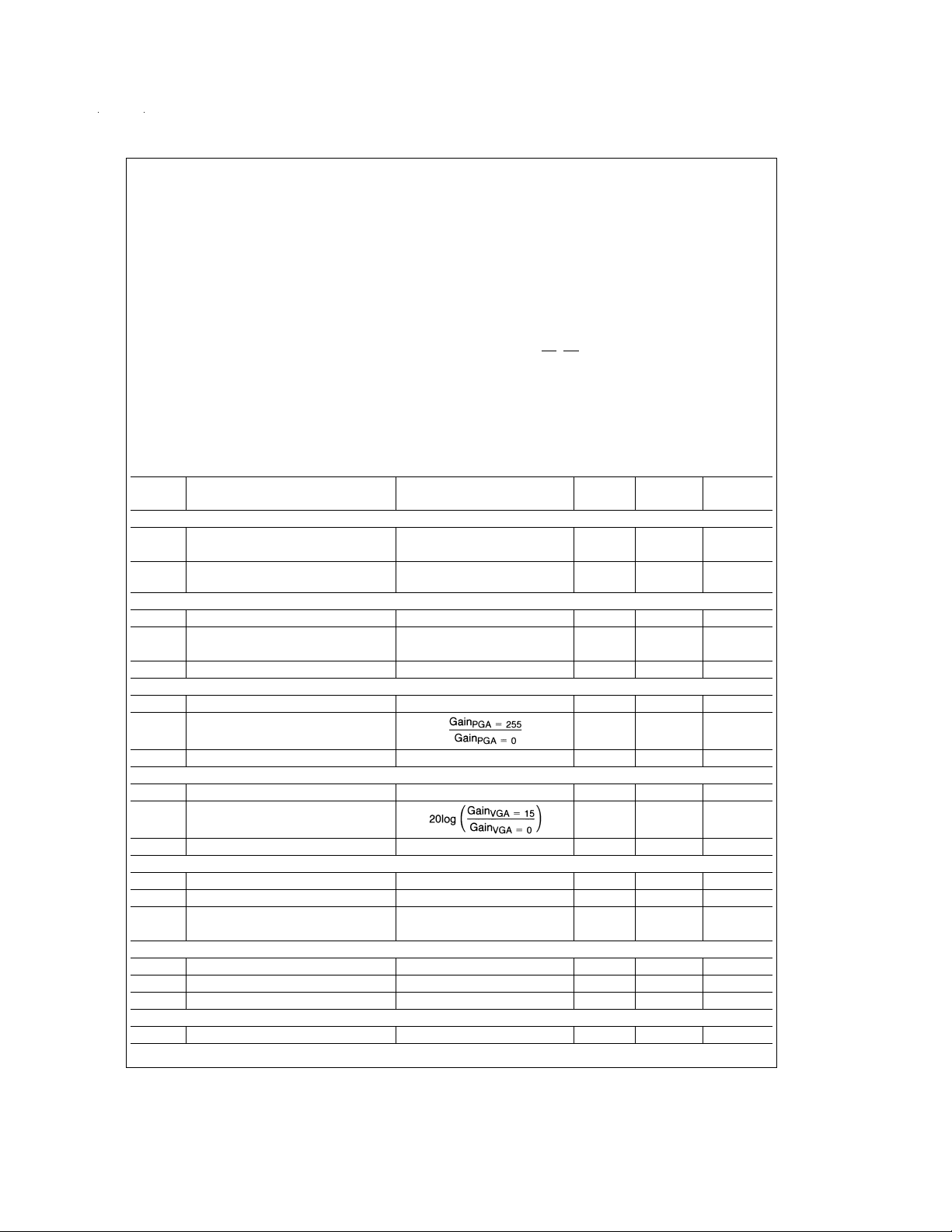
Electrical Characteristics
=
The following specifications apply for AGND=DGND=DGND(I/O)=0V, V
REF IN=+1.225V
apply for T
DC,fMCLK
=
=
T
A
J
=
20MHz, R
to T
T
MIN
MAX
=
25Ω. All LSB units are ADC LSBs unless otherwise specified. Boldface limits
S
; all other limits T
=
A
=
T
25˚C. (Note 8)
J
=
V
A
+5.0V
D
DC,VD(I/O)
Symbol Parameter Conditions Typical Limits Units
(Note 9) (Note 10) (Limits)
CCD SOURCE REQUIREMENTS FOR FULL SPECIFIED ACCURACY AND DYNAMIC RANGE (Note 11)
V
WHITE
Maximum Peak CCD Differential VGA Gain=0dB 1.1 V (min)
Signal Range VGA Gain=9dB 0.4 V (min)
V
RFT
Maximum CCD Reset FeedThrough
Amplitude
ADC CHARACTERISTICS (Note 16)
Resolution with No Missing Codes f
ILE Integral Linearity Error (Note 12) f
DNL Differential Non-Linearity f
=
12MHz 9 Bits (min)
MCLK
=
12MHz
MCLK
=
12MHz +2.0 LSB (max)
MCLK
PGA CHARACTERISTICS
Monotonicity 8 Bits (min)
=
+5.0 or +3.0V
,
DC
2 V (min)
+4.0 LSB (max)
−3.0 LSB (min)
MAX
PGA Adjustment Range
Gain Error at any Gain (Note 14) 1.4
VGA CHARACTERISTICS
Monotonicity 4 Bits (min)
VGA Adjustment Range
Gain Error at any Gain (Note 15)
OFFSET TRIM CHARACTERISTICS
Offset DAC LSB Size In Units of ADC LSBs 1.7 LSB
Offset DAC DNL In Units of Offset DAC LSBs
Offset Add Magnitude In Units of ADC LSBs 8
SYSTEM CHARACTERISTICS
Full Channel Gain Error VGA Gain=1, PGA Gain=1
Pre-PGA Offset Error (In ADC LSBs) VGA Gain=1, Offset DAC=0
Post-PGA Offset Error (In ADC LSBs) Offset Add=0
REFERENCE AND ANALOG INPUT CHARACTERSTICS (Note 7)
OS Input Capacitance 5 pF
2.95 2.8 V/V (min)
%
(max)
8.95 8.5 dB (min)
±
0.15 dB (max)
±
0.25
±
0.9 LSB
6.4 LSB (min)
10.0 LSB (max)
±
0.6
±
4 LSB
±
4 LSB
±
3.0
%
(max)
www.national.com3
Page 4
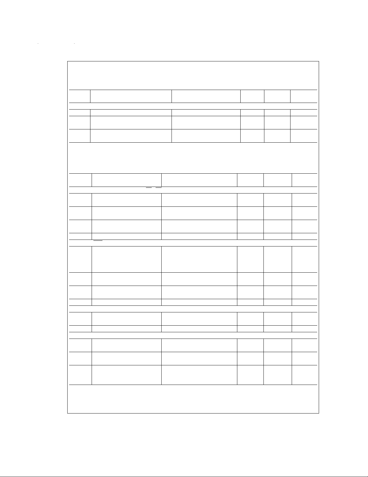
Electrical Characteristics (Continued)
=
The following specifications apply for AGND=DGND=DGND(I/O)=0V, V
REF IN=+1.225VDC,f
apply for T
=
=
T
A
J
=
20MHz, R
MCLK
to T
T
MIN
MAX
=
25Ω. All LSB units are ADC LSBs unless otherwise specified. Boldface limits
S
; all other limits T
=
A
=
T
25˚C. (Note 8)
J
=
V
A
+5.0V
D
DC,VD(I/O)
Symbol Parameter Conditions Typical Limits Units
(Note 9) (Note 10) (Limits)
REFERENCE AND ANALOG INPUT CHARACTERSTICS (Note 7)
OS Input Leakage Current Measured with OS=2.45V
R
REF
ADC Reference Ladder (REF OUT
to REF IN) Impedance 2000 Ω (max)
HI
DC
950
REF IN Reference Voltage (Note 13) 1.225
=
+5.0 or +3.0V
,
DC
2 20 nA (max)
500 Ω (min)
1.19 V (min)
1.26 V (max)
DC and Logic Electrical Characteristics
The following specifications apply for AGND=DGND=DGND
IN=+1.225V
25˚C.
DC,fMCLK
=
20MHz, R
=
25Ω. Boldface limits apply for T
s
(I/O)
=
Symbol Parameter Conditions Typical Limits Units
CD0–CD7, MCLK, SYNC, SDI, SCLK, CS , RD DIGITAL INPUT CHARACTERISTICS
=
V
5.25V 2.0 V (min)
V
IN(1)
V
IN(0)
I
IN
C
IN
Logical “1” Input Voltage
Logical “0” Input Voltage
Input Leakage Current
Input Capacitance 5 pF
D(I/O)
=
V
3.6V 2.0 V (min)
D(I/O)
=
V
4.75V 0.8 V (max)
D(I/O)
=
V
2.7V 0.7 V (max)
D(I/O)
=
V
V
IN
D
=
V
DGND −0.1 µA
IN
DD0–DD9, EOC , CCLK, SDO DIGITAL OUTPUT CHARACTERISTICS
=
V
4.75V, I
V
V
I
C
OUT
OUT(1)
OUT(0)
OUT
D(I/O)
=
V
Logical “1” Output Voltage
Logical “0” Output Voltage
TRI-STATE®Output Current V
(DD0–DD9 only) V
D(I/O)
=
V
D(I/O)
=
V
D(I/O)
=
V
D(I/O)
=
V
D(I/O)
=
OUT
=
OUT
TRI-STATE Output Capacitance 5 pF
OUT
4.75V, I
OUT
2.7V, I
OUT
2.7V, I
OUT
5.25V, I
OUT
3.6V, I
OUT
DGND 0.1 µA
V
D
φ1, φ2, RS, TR DIGITAL OUTPUT CHARACTERISTICS
V
V
OUT(1)
OUT(0)
Logical “1” Output Voltage
Logical “0” Output Voltage V
=
V
4.75V, I
D
=
V
4.75V, I
D
=
5.25V, I
D
OUT
OUT
OUT
=
=
=
POWER SUPPLY CHARACTERISTICS
I
A
I
D
I
D(I/O)
Analog Supply Current
Digital Supply Current
Digital I/O Supply Current
Operating 25 38 mA (max)
Standby 50 µA
Operating 6 8 mA (max)
Standby 65 µA
Operating, V
Operating, V
Standby, V
=
D(I/O)
=
D(I/O)
=
5.0V or 3.0V 1.7 mA
D(I/O)
=
0V, V
=
V
A
A
+5.0V
D
=
=
T
J
DC,VD(I/O)
to T
T
MIN
=
; all other limits T
MAX
+5.0 or +3.0V
A
, REF
DC
=
=
T
J
(Note 9) (Note 10) (Limits)
0.1 µA
=
−360 µA 2.4 V (min)
=
−10 µA 4.4 V (min)
=
−360 µA 2.1 V (min)
=
−10 µA 2.5 V (min)
=
1.6 mA 0.4 V (max)
=
1.6 mA 0.4 V (max)
−0.1 µA
−360 µA 2.4 V (min)
−10 µA 4.4 V (min)
1.6 mA 0.4 V (max)
5.0V 3.1 6 mA (max)
3.0V 1.6 4 mA (max)
www.national.com 4
Page 5
AC Electrical Characteristics, MCLK Independent
The following specifications apply for AGND=DGND=DGND
f
MCLK
=
T
MIN
=
20MHz, t
to T
MAX
=
1/f
MCLK
; all other limits T
MCLK,tr
=
=
t
f
=
=
T
A
J
5ns, R
25˚C.
s
=
25Ω,C
=
(I/O)
(databus loading)=50 pF/pin. Boldface limits apply for T
L
Symbol Parameter Conditions Typical Limits Units
f
MCLK
Maximum MCLK Frequency (Note 16) 20 MHz (min)
Minimum MCLK Frequency 1 MHz (max)
MCLK Duty Cycle
t
A
t
CDSETUP
t
CDHOLD
t
D1H,tD0H
t
DACC
f
SCLK
SYNC Setup of MCLK 5 10 ns (min)
Correction Data Valid to CLK Setup 14 20 ns (min)
Correction Data Valid to CLK Hold −12 0 ns (min)
RD High to DD0–DD9 TRI-STATE 5 15 ns (max)
Access Time Delay from RD Low to
DD0–DD9 Data Valid
Maximum SCLK Frequency 8 MHz (min)
SCLK Duty Cycle
t
SDI
t
HDI
t
DDO
t
HDO
t
DELAY
t
SETUP
t
S1H,tS0H
t
RDO
t
FDO
SDI Set-Up Time from SCLK
Rising Edge
SDI Hold Time from SCLK
Rising Edge
Delay from SCLK Falling Edge to
SDO Data Valid
SDO Hold Time from SCLK
Falling Edge
=
3k, C
R
L
DELAY from SCLK Falling Edge to CS
Rising or Falling Edge
Set-Up Time of CS Rising or Falling
Edge to SCLK Rising Edge
Delay from CS Rising Edge to SDO
TRI-STATE
SDO Rise Time, TRI-STATE to High
SDO Rise Time, Low to High 20 ns
SDO Fall Time, TRI-STATE to Low
SDO Fall Time, High to Low 20 ns
=
R
3k, C
L
=
3k, C
R
L
=
3k, C
R
L
=
=
0V, V
V
A
D
=
V
D(I/O)
, REF IN=+1.225VDC,
+5.0V
DC
(Note 9) (Note 10) (Limits)
30 40
70 60
15 30 ns (max)
40
60
3 10 ns (min)
2 15 ns (min)
25 55 ns (max)
=
25pF 30
L
55 ns (max)
5 ns (min)
5 10 ns (min)
0 10 ns (min)
=
50pF 25 50 ns (max)
L
=
50pF
L
=
50pF
L
20 ns
20 ns
%
%
%
%
=
A
(min)
(max)
(min)
(max)
T
J
AC Electrical Characteristics, MCLK Dependent
The following specifications apply for AGND=DGND=DGND
=
f
20MHz, t
MCLK
Register Parameters for limits labelled C.R. Boldface limits apply for T
25˚C.
MCLK
=
1/f
MCLK,tr
=
=
t
f
5ns, R
s
=
25Ω,C
=
(I/O)
(databus loading)=50 pF/pin. Refer to
L
Symbol Parameter Conditions Typical Limits Units
t
START
t
φ
t
TRWIDTH
t
GUARD
t
RSWIDTH
t
RS
MCLK to first φ1 High 50ns 1 t
φ1, φ2 Clock Period
Standard CCD Mode 400ns 8 t
Even/Odd CCD Mode 800ns 16 t
Transfer Pulse (TR) Width C.R. µs
φ1 to TR, TR to φ1 Guardband C.R. ns
Reset Pulse (RS) Width C.R. ns
Falling Edge of φ1 to RS Standard CCD Mode
Either Edge of φ1 to RS Even/Odd CCD Mode
0V, V
=
=
V
A
D
=
=
T
A
J
=
V
D(I/O)
to T
T
MIN
MAX
, REF IN=+1.225VDC,
+5.0V
DC
Table 2
; all other limits T
. Configuration
=
A
(Note 9) (Note 10) (Limits)
C.R. ns
www.national.com5
T
J
MCLK
MCLK
MCLK
=
Page 6
AC Electrical Characteristics, MCLK Dependent (Continued)
The following specifications apply for AGND=DGND=DGND
=
f
20MHz, t
MCLK
Register Parameters for limits labelled C.R. Boldface limits apply for T
25˚C.
MCLK
=
1/f
MCLK,tr
=
=
t
f
5ns, R
=
s
25Ω,C
=
(I/O)
(databus loading)=50 pF/pin. Refer to
L
Symbol Parameter Conditions Typical Limits Units
t
S/HREF
t
S/HSIG
t
S/HWIDTH
t
SYNCLOW
t
B
t
CCLKWIDTH
t
DATAVALID
t
EOCWIDTH
Falling Edge of φ1 to Ref. Sample Standard CCD Mode
Either Edge of φ1 to Ref. Sample Even/Odd CCD Mode
Falling Edge of φ1 to Sig. Sample Standard CCD Mode
Either Edge of φ1 to Sig. Sample Even/Odd CCD Mode
Sample Pulse Width
(Acquisition Time)
SYNC Low Between Lines 100ns 2 t
SYNC Setup of φ1 to End Line 2 t
CCLK Pulse Width 250ns 5 t
Data Valid Time from EOC Low 300 ns (min)
EOC Pulse Width 250ns 5 t
φ1 and φ2 Frequency
Standard CCD Mode 2.5MHz f
Even/Odd CCD Mode 1.25MHz f
φ1 and φ2 Duty Cycle 50
0V, V
=
=
V
A
D
=
=
T
A
J
=
V
D(I/O)
to T
T
MIN
MAX
, REF IN=+1.225VDC,
+5.0V
DC
Table 2
; all other limits T
. Configuration
=
T
A
J
(Note 9) (Note 10) (Limits)
C.R. ns
C.R. ns
50ns 1 t
/8 Hz
MCLK
/16 Hz
MCLK
MCLK
MCLK
MCLK
MCLK
MCLK
%
Electrical Characteristics (Notes)
Note 1: Absolute Maximum Ratings indicate limits beyond which damage to the device may occur. Operating Ratings indicate conditions for which the device is
functional, but do not guarantee specific performance limits. For guaranteed specifications and test conditions, see the Electrical Characteristics. The guaranteed
specifications apply only for the test conditions listed. Some performance characteristics may degrade when the device is not operated under the listed test conditions.
Note 2: All voltages are measured with respect to GND=AGND=DGND=DGND
Note 3: When the input voltage (V
The 50 mA maximum package input current rating limits the number of pins that can simultaneously safely exceed the power supplies with an input current of 25
mA to two.
Note 4: The maximum power dissipation must be derated at elevated temperatures and is dictated by T
allowable power dissipation at any temperature is P
mounted is 52˚C/W for the V52A PLCC package, and 70˚C/W for the VEG52A TQFP package.
Note 5: Human body model, 100pF capacitor discharged through a 1.5 kΩ resistor.
Note 6: See AN450 “Surface Mounting Methods and Their Effect on Product Reliability” or the section titled “Surface Mount” found in any National Semiconductor
Linear Data Book for other methods of soldering surface mount devices.
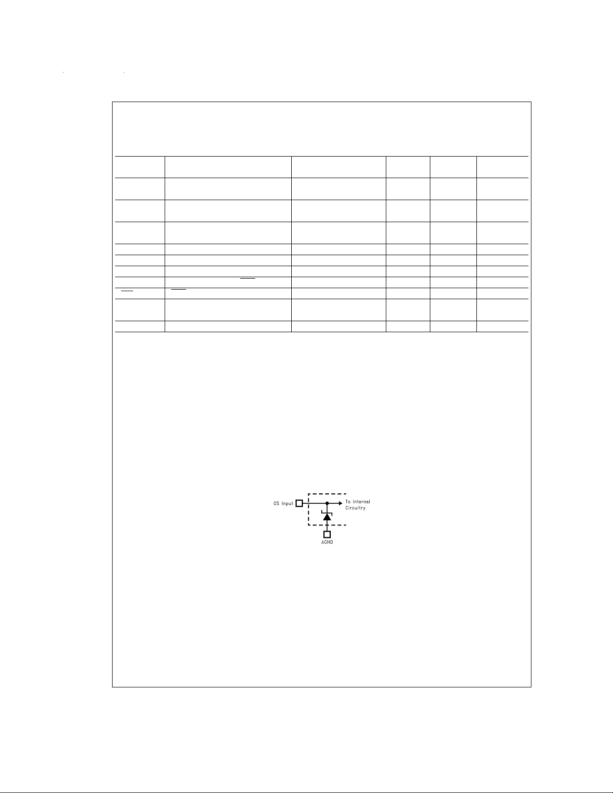
Note 7: AZener diode clamps the OS analog input to AGND as shown below. This input protection, in combination with the external clamp capacitor and the output
impedance of the CCD, prevents damage to the LM9811 from transients during power-up.
) at any pin exceeds the power supplies (V
IN
=
D
(T
Jmax–TA
)/θJA.T
Jmax
=
0V, unless otherwise specified.
(I/O)
<
GND or V
IN
=
150˚C for this device. The typical thermal resistance (θ
>
VAor VD), the current at that pin should be limited to 25 mA.
IN
, θJAand the ambient temperature, TA. The maximum
Jmax
) of this part when board
JA
=
(min)
(max)
Note 8: Toguarantee accuracy, it is required that V
Note 9: Typicals are at T
Note 10: Tested limits are guaranteed to National’s AOQL (Average Outgoing Quality Level).
=
=
T
25˚C, f
J
A
and VDbe connected together to the same power supply with separate bypass capacitors at each supply pin.
A
=
20MHz, and represent most likely parametric norm.
MCLK
www.national.com 6
DS012813-4
Page 7
Electrical Characteristics (Notes) (Continued)
Note 11: For CCDs, V
pixel output voltage for a white (full scale) image with respect to the reference level, V
reset feedthrough pulse. For CIS, V
correctable range of pixel-to-pixel V
the LM9811 can correct for using its internal PGA.
is defined as the CCD OS voltage for the reference period following the reset feedthrough pulse. V
BLACK
is defined as the peak CCD pixel output voltage for a white (full scale) image with respect to GND (0V). The maximum
WHITE
variation is defined as the maximum variation in V
WHITE
BLACK-VRFT
WHITE
is defined as the peak CCD
is defined as the peak positive deviation above V
(due to PRNU, light source intensity variation, optics, etc.) that
WHITE
BLACK
of the
CCD Output Signal
DS012813-5
Note 12: Integral linearity error is defined as the deviation of the analog value, expressed in LSBs, from the straight line that best fits the actual transfer function
of the ADC.
Note 13: Reference voltages below 1.19V may decrease SNR. Reference voltages above 1.26V may cause clipping errors inside the LM9811. The
LM4041EIM3-1.2 (SOT-23 package) or the LM4041EIZ-1.2 (TO-92 package) bandgap voltage references are recommended for this application.
Note 14: PGA Gain Error is the maximum difference between the measured gain for any PGA code and the ideal gain calculated by using the formula
Note 15: VGA Gain Error is the maximum difference between the measured gain for any VGA code and the ideal gain calculated by using the formula
Note 16: ADC Characteristics (Resolution, INL and DNL) are guaranteed for f
except ADC Characteristics, which will be approximately 8 bits.
and PGA RANGE=the PGA adjustment range (in V/V) of the LM9811 under test.
and VGA RANGE=the VGA adjustment range (in dB) of the LM9811 under test.
up to 12MHz. For 12MHz<f
MCLK
CIS Output Signal
≤ 20 MHz, all specifications are guaranteed
MCLK
DS012813-6
Typical Performance Characteristics
φ1, φ2, RS, and TR Rise and Fall Times
Through a Series Resistance vs Load Capacitance
DS012813-8
www.national.com7
Page 8
Pin Descriptions
CCD Driver Signals
φ1 Digital Output. CCD clock signal, phase
φ2 Digital Output. CCD clock signal, phase
RS Digital Output. Reset pulse for the CCD.
TR Digital Output. Transfer pulse for the
OS Analog Input. This is the OS (Output
REF IN Analog Inputs. These two pins are the
REF OUT
REF OUT
,
V
TEST1
V
TEST2
SDI Digital Input. Serial Data Input pin.
SDO Digital Output. Serial Data Output pin.
SCLK Digital Input. This is the serial data
CS
CD0 (LSB)–
CD7 (MSB)
1.
2.
CCD.
Analog I/O
Signal) from the CCD. The maximum
peak signal that can be accurately
digitized is equal to the voltage at REF
IN, typically 1.225V.
system reference voltage inputs and
should be tied together to a 1.225V
voltage source and bypassed to AGND
with a 0.1 µF monolithic capacitor.
Analog Output. This reference voltage is
HI
developed internally by the LM9811,
and is equal to 3 times REF IN. It
should be bypassed to AGND with a
0.1 µF monolithic capacitor.
Analog Output. This reference voltage is
MID
developed internally by the LM9811,
and is equal to 2 times REF IN. It
should be bypassed to AGND using a
0.1 µF monolithic capacitor.
Analog Inputs/Outputs. These pins are
used for testing the device during
manufacture and should be left
unconnected.
Configuration Register I/O
clock, used to clock data in through SDI
and out through SDO. SCLK is
asynchronous to MCLK. Input data is
latched and output data is changed on
the rising edge of SCLK.
Digital Input. This is the Chip Select
signal for writing to the Configuration
Register through the serial interface.
This input must be low in order to
communicate with the Configuration
Register. This pin is used for serial I/O
only–it has no effect on any other
section of the chip.
Digital Coefficient I/O
Digital Inputs. Correction Coefficient
Databus. This is the 8-bit data path for
the gain adjust PGA, used during line
scan.
CCLK Digital Output. This is the signal that is
used to clock the Gain coefficients into
the LM9811. Data is latched on the
rising edge of CCLK.
Digital Output I/O
DD0 (LSB)–
DD9 (MSB)
Digital Outputs. Pixel Output Databus.
This data bus outputs the 10-bit digital
output data during line scan.
EOC
Digital Output. This is the End of
Conversion signal from the ADC
indicating that new pixel data is
available.
RD
Digital Input. Taking this input low
places the data stored in the output
latch on the bus. When this input is high
the DD0–DD9 bus is in TRI-STATE.
General Digital I/O
MCLK Digital Input. This is the 12MHz (typical)
master system clock.
SYNC Digital Input. A low-to-high transition on
this input begins a line scan operation.
The line scan operation terminates
when this input is taken low.
Analog Power
V
A
This is the positive supply pin for the
analog supply. It should be connected
to a voltage source of +5V and
bypassed to AGND with a 0.1 µF
monolithic capacitor in parallel with a
10 µF tantalum capacitor.
AGND This is the ground return for the analog
supply.
Digital Power
V
D
This is the positive supply pin for the
digital supply. It should be connected to
a voltage source of +5V and bypassed
to DGND with a 0.1 µF monolithic
capacitor.
DGND This is the ground return for the digital
supply.
V
D(I/O)
This is the positive supply pin for the
digital supply for the LM9811’s I/O. It
should be connected to a voltage
source of +3V to +5V and bypassed to
DGND
capacitor. If the supply for this pin is
different than the supply for V
it should also be bypassed with a 10 µF
with a 0.1 µF monolithic
(I/O)
and VD,
A
tantalum capacitor.
DGND
(I/O)
This is the ground return for the digital
supply for the LM9811’s I/O.
NC
NC All pins marked NC (no connect) should
be left floating. Do not tie NC pins to
ground., power supplies, or any other
potential or signal.
www.national.com 8
Page 9
Timing Diagrams
DS012813-9
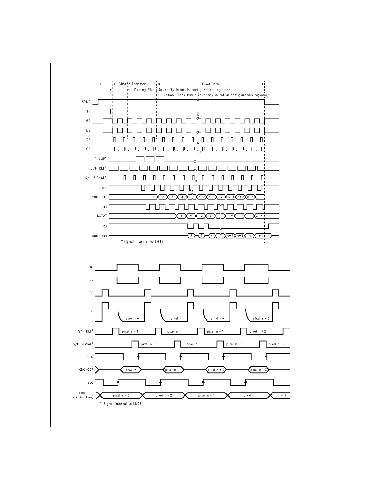
FIGURE 1. Line Scan Timing Overview
FIGURE 2. Pixel Pipeline Timing Overview
DS012813-10
www.national.com9
Page 10
Timing Diagrams (Continued)
FIGURE 4. Timing for End of Line/Start of Next Line
DS012813-11
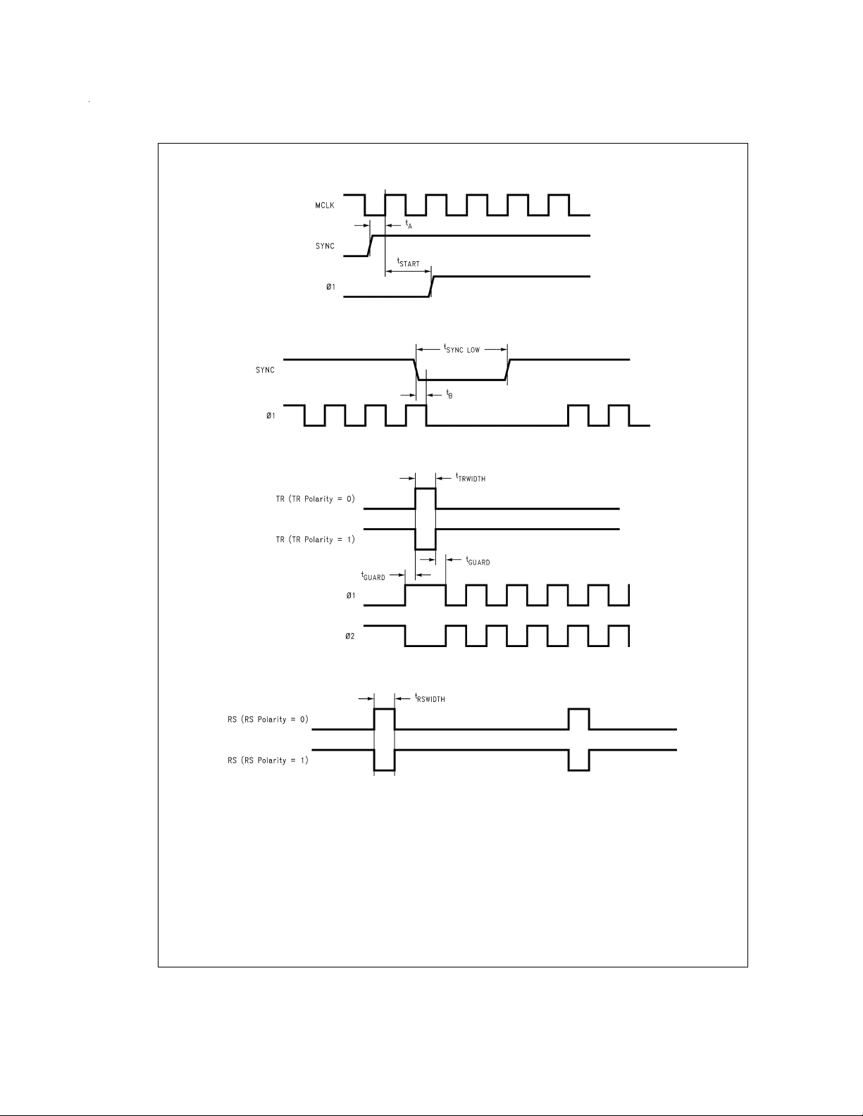
FIGURE 3. Timing for Start of Line Scan
DS012813-12
FIGURE 5. TR Pulse Timing
FIGURE 6. RS Pulse Polarity
www.national.com 10
DS012813-13
DS012813-14
Page 11
Timing Diagrams (Continued)
Note: Clamp signal only active during optical black pixels at beginning of line.
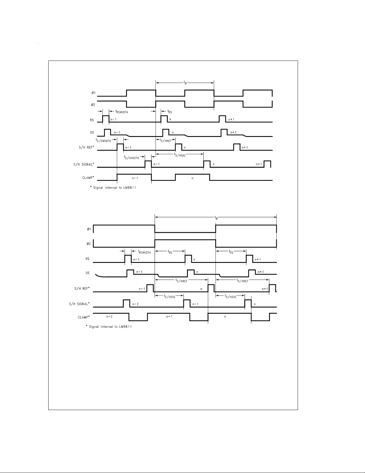
FIGURE 7. CCD Timing
Note: Clamp signal only active during optical black pixels at beginning of line.
FIGURE 8. CCD Timing (Even/Odd CCDs)
DS012813-15
DS012813-16
www.national.com11
Page 12

Timing Diagrams (Continued)
i=value programmed in Dummy Pixel Register - 1 (for example: Dummy Pixel Register=17→i=16→16 Dummy Pixel).
j=value programmed in Optical Black Register.
FIGURE 9. Dummy Pixel and Optical Black Pixel Timing
FIGURE 10. Coefficient Data Timing
DS012813-17
DS012813-18
FIGURE 11. Output Data Timing
www.national.com 12
DS012813-19
Page 13

Timing Diagrams (Continued)
FIGURE 12. Data Timing (Output and Coefficient Data Sharing Same Bus)
Serial Configuration Register Timing Diagrams
DS012813-20
FIGURE 13. Configuration Register Write Timing using CS, Continuous SCLK (16-Bit Word)
FIGURE 14. Configuration Register Read Timing using CS, Continuous SCLK (16-Bit Word)
DS012813-21
DS012813-22
www.national.com13
Page 14

Serial Configuration Register Timing Diagrams (Continued)
FIGURE 15. SDO Timing
FIGURE 16. Configuration Register Write Timing with CS Continuously Low (16-Bit Word)
FIGURE 17. Configuration Register Write Timing with CS Continuously Low (Two 8-Bit Bytes)
DS012813-23
DS012813-24
DS012813-25
FIGURE 18. Configuration Register Read Timing with CS Continuously Low (16-Bit Word)
FIGURE 19. Configuration Register Read Timing with CS Continuously Low (Two 8-Bit Bytes)
www.national.com 14
DS012813-26
DS012813-27
Page 15

Configuration Register t
20MHz (t
=
50ns). Times for 12MHz MCLK can be calculated by multiplying by
MCLK
MCLK
=
=
1/f
1 MCLK period. Examples given in parenthesis are for f
MCLK
MCLK
=
TABLE 1. Configuration Register Address Table
A2 A1 A0 D7 D6 D5 D4 D3 D2 D1 D0
000
Standard
Mode or
Even/Odd
Mode
RS
Pulse
Width
RS
Pulse
Polarity
RS Pulse Position
MODE RSW1 RSW0 RSPOL RSPOS3 RSPOS2 RSPOS1 RSPOS0
001
Sample Reference Position
(Maximum Register Value is 14)
Sample Signal Position
SR3 SR2 SR1 SR0 SS3 SS2 SS1 SS0
010
φ1 φ2RSTR
Enable Enable Enable Enable Guardband Polarity
TR Pulse Width
TR–φ1TR
φ1EN φ2EN RSEN TREN TRW1 TRW0 TRGRD TRPOL
0 1 1 Signal
Polarity
Dummy Pixels (Minimum Register Value is 2)
SIGPOL BLS6 BLS5 BLS4 BLS3 BLS2 BLS1 BLS0
100
101
110
BLL7 BLL6 BLL5 BLL4 BLL3 BLL2 BLL1 BLL0
GAIN7 GAIN6 GAIN5 GAIN4 GAIN3 GAIN2 GAIN1 GAIN0
PGA Gain
Source
Offset
DAC
Sign
Optical Black Pixels (Minimum Register Value is 1)
PGA Gain Coefficient
Power-
down
Offset
Add
VGA Gain
MSB
VGA
Gain
VGA
Gain
VGA Gain
LSB
PGASRC ODSIGN PD OFFADD VGA3 VGA2 VGA1 VGA0
111
Offset
MSB LSB
Offset
DAC
Offset
DAC
Offset
Test ModesDAC DAC
VOS3 VOS2 VOS1 VOS0 0000
TABLE 2. Configuration Register Parameters
Parameter Control Bits Result
MODE
MODE
0 Standard CCD (φ frequency=f
1 Even/Odd CCD (φ frequency=f
RS Pulse Width
)
(t
RSWIDTH
RS1 RS0
00 1t
01 2t
10 3t
11 4t
RS Pulse Polarity RSPOL
0 RS
1 RS
MCLK
MCLK
MCLK
MCLK
MCLK
MCLK
www.national.com15
/8)
/16)
(50ns)
(100ns)
(150ns)
(200ns)
Page 16

Configuration Register t
20MHz (t
=
50ns). Times for 12MHz MCLK can be calculated by multiplying by
MCLK
MCLK
=
=
1/f
1 MCLK period. Examples given in parenthesis are for f
MCLK
(Continued)
TABLE 2. Configuration Register Parameters (Continued)
Parameter Control Bits Result
RSPOS3 RSPOS2 RSPOS1 RSPOS0
0 0 0 0 0.0t
0 0 0 1 0.5t
0 0 1 0 1.0t
0 0 1 1 1.5t
0 1 0 0 2.0t
0 1 0 1 2.5t
RS Pulse Position
)
(t
RS
0 1 1 0 3.0t
0 1 1 1 3.5t
1 0 0 0 4.0t
1 0 0 1 4.5t
1 0 1 0 5.0t
1 0 1 1 5.5t
1 1 0 0 6.0t
1 1 0 1 6.5t
1 1 1 0 7.0t
1 1 1 1 7.5t
SR3 SR2 SR1 SR0
0 0 0 0 0.0t
0 0 0 1 0.5t
0 0 1 0 1.0t
0 0 1 1 1.5t
0 1 0 0 2.0t
0 1 0 1 2.5t
Sample Reference
Position (t
S/HREF
)
0 1 1 0 3.0t
0 1 1 1 3.5t
1 0 0 0 4.0t
1 0 0 1 4.5t
1 0 1 0 5.0t
1 0 1 1 5.5t
1 1 0 0 6.0t
1 1 0 1 6.5t
1 1 1 0 7.0t
1 1 1 1 Not Valid
MCLK
MCLK
MCLK
MCLK
MCLK
MCLK
MCLK
MCLK
MCLK
MCLK
MCLK
MCLK
MCLK
MCLK
MCLK
MCLK
MCLK
MCLK
MCLK
MCLK
MCLK
MCLK
MCLK
MCLK
MCLK
MCLK
MCLK
MCLK
MCLK
MCLK
MCLK
MCLK
=
(0ns)
(25ns)
(50ns)
(75ns)
(100ns)
(125ns)
(150ns)
(175ns)
(200ns)
(225ns)
(250ns)
(275ns)
(300ns)
(325ns)
(350ns)
(375ns)
(0ns)
(25ns)
(50ns)
(75ns)
(100ns)
(125ns)
(150ns)
(175ns)
(200ns)
(225ns)
(250ns)
(275ns)
(300ns)
(325ns)
(350ns)
www.national.com 16
Page 17

Configuration Register t
20MHz (t
=
50ns). Times for 12MHz MCLK can be calculated by multiplying by
MCLK
MCLK
=
=
1/f
1 MCLK period. Examples given in parenthesis are for f
MCLK
(Continued)
TABLE 2. Configuration Register Parameters (Continued)
Parameter Control Bits Result
SS3 SS2 SS1 SS0
0 0 0 0 0.0t
0 0 0 1 0.5t
0 0 1 0 1.0t
0 0 1 1 1.5t
0 1 0 0 2.0t
0 1 0 1 2.5t
Sample Signal
Position (t
S/HSIG
)
0 1 1 0 3.0t
0 1 1 1 3.5t
1 0 0 0 4.0t
1 0 0 1 4.5t
1 0 1 0 5.0t
1 0 1 1 5.5t
1 1 0 0 6.0t
1 1 0 1 6.5t
1 1 1 0 7.0t
1 1 1 1 7.5t
φ1EN
φ1 Enable
0 φ1 Output Off
1 φ1 Output On
φ2EN
φ2 Enable
0 φ2 Output Off
1 φ2 Output On
RSEN
RS Enable
0 RS Output Off
1 RS Output On
TREN
TR Enable
0 TR Output Off
1 TR Output On
TRW1 TRW0
TR Pulse Width
)
(t
TRWIDTH
0 0 20 t
0 1 30 t
1 0 40 t
1 1 50 t
TR-φ1 TRGRD
Guardband 0 1t
(t
)1 2t
GUARD
TRPOL
TR Polarity
0 TR
1 TR
SIGPOL
Single Polarity
0 Positive (CIS)
1 Negative (CCD)
MCLK
MCLK
MCLK
MCLK
MCLK
MCLK
MCLK
MCLK
MCLK
MCLK
MCLK
MCLK
MCLK
MCLK
MCLK
MCLK
MCLK
MCLK
MCLK
MCLK
MCLK
MCLK
MCLK
=
(0ns)
(25ns)
(50ns)
(75ns)
(100ns)
(125ns)
(150ns)
(175ns)
(200ns)
(225ns)
(250ns)
(275ns)
(300ns)
(325ns)
(350ns)
(375ns)
(1.0 µs)
(1.5 µs)
(2.0 µs)
(2.5 µs)
(50ns)
(100ns)
www.national.com17
Page 18

Configuration Register t
20MHz (t
=
50ns). Times for 12MHz MCLK can be calculated by multiplying by
MCLK
MCLK
=
=
1/f
1 MCLK period. Examples given in parenthesis are for f
MCLK
MCLK
=
(Continued)
TABLE 2. Configuration Register Parameters (Continued)
Parameter Control Bits Result
BLS6 BLS5 BLS4 BLS3 BLS2 BLS1 BLS0 Dummy Pixels
Dummy Pixels
Note: Minimum
Register Value is 2.
Actual number of
dummy pixels in CCD
should be one less
than number in this
register.
0 000000 NotValid
0 000001 NotValid
0 000010 1
0 000011 2
••••••• •
1 111101 124
1 111110 125
1 111111 126
BLL7 BLL6 BLL5 BLL4 BLL3 BLL2 BLL1 BLL0 Optical Black Pixels
0 0000000 NotValid
0 0000001 1
Optical Black Pixels
Note: Minimum
Register Value is 1.
0 0000010 2
0 0000011 3
•••••••• •
1 1111101 253
1 1111110 254
1 1111111 255
GAIN7 GAIN6 GAIN5 GAIN4 GAIN3 GAIN2 GAIN1 GAIN0 dB [V/V]
0 0000000 0.00 1.000
0 0000001 0.07 1.008
Internal PGA
Gain Coefficient
0 0000010 0.13 1.015
•••••••• •
1 1111101 9.35 2.935
1 1111110 9.37 2.942
1 1111111 9.40 2.950
PGA Gain PGASRC
Coefficient 0 Internal
Source 1 External
ODSIGN
Offset DAC Sign
0 Negative
1 Positive
PD
Power Down
0 Operating
1 Powered Down
OFF ADD
Offset Add
0 Offset
1 Offset
z
z
+8 LSB
0 LSB
www.national.com 18
Page 19

Configuration Register t
20MHz (t
=
50ns). Times for 12MHz MCLK can be calculated by multiplying by
MCLK
MCLK
=
=
1/f
1 MCLK period. Examples given in parenthesis are for f
MCLK
(Continued)
TABLE 2. Configuration Register Parameters (Continued)
Parameter Control Bits Result
VGA3 VGA2 VGA1 VGA0 dB [V/V]
0 0 0 0 0.00 1.00
0 0 0 1 0.60 1.07
0 0 1 0 1.20 1.15
0 0 1 1 1.79 1.23
0 1 0 0 2.39 1.32
0 1 0 1 2.99 1.41
0 1 1 0 3.59 1.51
VGA Gain
0 1 1 1 4.19 1.62
1 0 0 0 4.79 1.74
1 0 0 1 5.38 1.86
1 0 1 0 5.98 1.99
1 0 1 1 6.58 2.13
1 1 0 0 7.18 2.29
1 1 0 1 7.78 2.45
1 1 1 0 8.38 2.62
1 1 1 1 8.97 2.81
MCLK
=
www.national.com19
Page 20

Configuration Register t
20MHz (t
=
50ns). Times for 12MHz MCLK can be calculated by multiplying by
MCLK
MCLK
=
=
1/f
1 MCLK period. Examples given in parenthesis are for f
MCLK
(Continued)
TABLE 2. Configuration Register Parameters (Continued)
Parameter Control Bits Result
ODSIGN VOS3 VOS2 VOS1 VOS0 Offset (LSB)
0 0000 0
0 0001 −1.68
0 0010 −3.36
0 0011 −5.04
0 0100 −6.72
0 0101 −8.40
0 0110 −10.08
0 0111 −11.76
0 1000 −13.44
0 1001 −15.12
0 1010 −16.80
0 1011 −18.48
0 1100 −20.16
0 1101 −21.84
0 1110 −23.52
Offset DAC
0 1111 −25.20
1 0000 0
1 0001 +1.68
1 0010 +3.36
1 0011 +5.04
1 0100 +6.72
1 0101 +8.40
1 0110 +10.08
1 0111 +11.76
1 1000 +13.44
1 1001 +15.12
1 1010 +16.80
1 1011 +18.48
1 1100 +20.16
1 1101 +21.84
1 1110 +23.52
1 1111 +25.20
MCLK
=
www.national.com 20
Page 21

Block Diagram of LM9811-Based System
Power supplies and bypass capacitors not shown for clarity.
FIGURE 20. LM9811 System Block Diagram
Applications Information
1.0 THEORY OF OPERATION
The LM9811 removes errors fromand digitizes alinear CCD
pixel stream, while providing all the necessary clock signals
to drive the CCD. Offset and gain errors for individual pixels
are removed at the pixel rate. Offset errors are removed
through correlated double sampling (CDS). Gain errors
(which may come from any combination of PRNU, uneven illumination, cos
moved through the use of a 8-bit programmable gain amplifier (PGA) in front of the ADC.
1.1 The Analog Signal Path
(See Block Diagram)
The analog output signal from the CCD is connected to the
OS Input of the LM9811 through a 0.01 µF (typical, seeSection 4.2,
During the CCD’s optical black pixel segment at the beginning of every line, this input is clamped to the REF OUT
voltage (approximately 2.45V). This DC restore operation
fixes the reference level of the CCD pixel stream at REF
OUT
MID
The signal is then buffered and fed to a digitally-programmed
4-bit VGA (variable gain amplifier). The gain of the VGA is
digitally programmable in 16 steps from 1V/V to 3V/V. The
VGAis used to compensate for peak white CCD outputs less
than the 1.225V full-scale required by the LM9811 for maximum dynamic range. When used with parallel output CCDs,
the VGA can fine-tune the amplitude of the red, green, and
blue signals. For a detailed explanation of the VGA, see Section 4.3.
The output of the VGA goes into the CDS (Correlated Double
Sampling) stage, consisting of two sample/hold amplifiers:
S/H Ref (Reference) and S/H Signal. The reference level of
the signal is sampled and held by the S/H Refcircuit and the
active pixel data is sampled and held by the S/H Signal circuit. The output of S/H Ref is subtractedfrom the S/HSignal
4
effect, RGB filter mismatch, etc.) are re-
Clamp Capacitor Selection
) DC blocking capacitor.
.
MID
DS012813-28
output and amplified by 2. The full-scale signal range at this
point is approximately 2.45Vp-p. CDS reduces or eliminates
many sources of noise, including reset noise, flicker noise,
and both high and low frequency pixel-to-pixel offset variation. For more information on the CDS stage, see Section
4.4.
At this point an offset voltage can be injected by the 5-bit (4
bits + sign) Offset DAC. This voltage is designed to compensate for any small fixed DC offset introduced by the CDS
S/Hs and the x2 amplifier. The LSB size of the DAC is approximately 1.7 ADC LSBs (4 mV). The adjustment range is
±
25 ADC LSBs. For a detailed explanation of the Offset
DAC, see Section 4.6.
The next stage is the PGA. This is a programmable gain am-
plifier that changes the gain
at the pixel rate
to correct for
gain errors due to PRNU, uneven illumination (such as cos
effect), RGB filter mismatch, etc.The gain adjustment range
is 0 dB to 9 dB (1V/V to 3V/V) with 8 bits of resolution. The
gain data (correction coefficients) is provided on the
CD0–CD7 bus. The gain may also be fixed at any value between 0 dB and 9 dB with the PGA Gain Coefficient configuration register. For additional information on the PGA,
see Section 4.7.
An approximately 8 LSB (19 mV) offset can be added at the
output of the PGA stage if necessary to ensure that the offset
is greater than zero. This eliminates the possibility of a negative offset clipping the darkest output pixels. For more information on the Offset Add Bit, see Section 4.8.
Finally, the output of the PGA is digitized by the ADC and
made available on the DD0–DD9 bus (Section 4.9).
Three reference voltages are used throughout the signal
path: the externally supplied REF IN (1.225V), and the internally generated REF OUT
(3.675V).
(2.45V) and REF OUT
MID
4
HI
www.national.com21
Page 22

Applications Information (Continued)
1.2 The CCD Clocking Signals
To maximize the flexibility of the LM9811, the CCD’s φ1, φ2,
RS, and TR pulses are internally generated, with a wide
range of options, making these signals compatible with most
commercial linear CCDs. In many cases, these output signals can drive the CCD clock inputs directly,with only series
resistors (for slew rate control) between the LM9811’s outputs and the CCD clock inputs.
1.3 The Digital Interface
There are three main sections to the digital interface of the
LM9811: a serial interface to the Configuration Register,
where all device programming is done, an 8 bit-wide input
databus for gain correction coefficients with a synchronous
clock output (CCLK), and a 10-bit output databus for the final
pixel output data with a synchronous end of conversion output signal (EOC) and an output enable input (RD). Please
note that the CS input affects only the serial I/O–it has no effect on the output databus, input coefficient bus, or any other
section of the LM9811.
2.0 DIGITAL INTERFACE
2.1 Reading and Writing to the Configuration Register
Communication with the Configuration Register is done
through a standard MICROWIRE
terface is also compatible with the Motorola SPI
and is simple enough to easily be implemented in custom
hardware if needed.
The serial interface timing is shown in
Figures 16, 17, 18, 19
(Please note that some microcontrollers output data MSB
first. When using these microcontrollers the bits in the configuration register are effectively reversed.) Input data is
latched on the rising edge of SCLK, and output data changes
on the falling edge of SCLK. CS must be low to enable serial
I/O.
If SCLK is only clocked whensending or receiving data from
the LM9811, and held low at all other times, then CS can be
tied low permanently as shown in
SCLK is continuous, then CS must be usedto determine the
beginning and the end of a serial byte or word (see
13, 14
). Note that CS must make its high-to-low and
low-to-high transitions when SCLK is low, otherwise the internal bit counter may receive an erroneous pulse, causing
an error in the write or read operation.
Data may be transmitted and received in two 8-bit bytes
(typical with microcontroller interfaces) or one 16-bit word
(for custom serial controllers).
The Configuration Register is programmed by sending a
control byte to the serial port. This byte indicates whether
this is a read or a write operation, and gives the 3-bit address
of the register bank to be read from or written to. If this is a
read operation, the next 8 SCLKs will output the data at the
requested location on the SDO pin. If this is a write operation, the data to be sent to the specified location should be
clocked in on the SDI input duringthe next 8 SCLKs. Data is
sent and received using the LSB (Least Significant Bit) first
format.
For maximum system reliability, each configuration register
location can be read back and verified after a write.
™
serial interface. This in-
. Data is sent serially, LSB first.
™
standard
Figures 13, 14
and
Figures 16, 17, 18, 19
Figures
.If
If the serial I/O to the configuration register falls out of sync
for any reason, it can be reset by sending 8 or more SCLKs
with CS held high.
2.2 Writing Correction Coefficient Data on the
CD0–CD7 Bus
Correction coefficient data for each pixel is latched on the
rising edge of the CCLK output signal (see
that there is a 3 pixel latency between when the coefficient
data is latched and when the output data is available. As
ure 2
,
Pixel Pipeline Timing Overview
for pixel n is latched shortly before the output data for pixel
n-2 becomes available on the output databus (DD0–DD9).
Note that there is no way to provide a correction coefficient
for pixel 1, the first pixelin the CCD array. This is usually not
a problem since the first several pixels of a CCD are usually
optical black pixels, and used for clamping.
2.3 Reading Output Data on the DD0–DD9 Bus
The corrected digital output data representing each pixel is
available on the DD0–DD9 databus. The data is valid after
the falling edge of the EOC output. The RD input takes the
databus in and out of TRI-STATE. RD can be held low at all
times if there are noother devicesneeding the bus, or it can
be used to TRI-STATE the bus between pixels, allowing
other devices access to the bus.
(Output and Coefficient Data Sharing Same Bus)
how EOC can be tied to RD to automatically multiplex between coefficient data and conversion data.
2.4 MCLK
This is the master clock input that controls the LM9811. The
pixel conversion rate is fixed at 1/8 of this frequency.Many of
the timing parameters are also relative to the frequency of
this clock.
2.5 SYNC
This input signals the beginning of a line. When SYNC goes
high, the LM9811 generates a TR pulse, then begins converting pixels until the SYNC line is brought low again. Since
there is no pixel counter in the LM9811, it will work with
CCDs of any length.
3.0 DIGITAL CCD INTERFACE
3.1 Buffering φ1, φ2, RS, and TR
The LM9811can drive the φ1, φ2, RS, and TR inputs of many
CCDs directly, without the need for external buffersbetween
the LM9811 and the CCD. Most linear CCDs designed for
scanner applications require 0V to 5V signal swings into
20pF to 500pF input loading. Series resistors are typically inserted between the driver and the CCD to control slew rate
and isolate the driver from the large load capacitances. The
values of these resistors are usually given in the CCD’s
datasheet.
4.0 ANALOG INTERFACE
4.1 Voltage Reference
The two REF IN pinsshould beconnected to a 1.225V
reference voltage capable of sinking between 2 mA and
5 mA of current coming from the 500Ω–1400Ω resistor string
between REF OUT
bandgap reference is recommended for this application as
shown in
Figure 21
and REF IN. The LM4041-1.2 1.225V
HI
. The inexpensive “E” grade meets all the
Figure 10
). Note
Fig-
shows, coefficientdata
Figure 12,Data Timing
, shows
±
2
%
www.national.com 22
Page 23

Applications Information (Continued)
requirements of the application and is available in a TO-92
(LM4041EIZ-1.2) package as well as a SOT-23 package
(LM4041EIM3-1.2) to minimize board space.
Due to the transient currents generated by the LM9811’s
ADC, PGA, and CDS circuitry, the REF IN pins, the REF
OUT
pin and the REF OUTHIpin should all be bypassed
MID
to AGND with 0.1 µF monolithic capacitors.
DS012813-29
FIGURE 21. Voltage Reference Generation
4.2 Clamp Capacitor Section
This section is very long because it is relatively complicated
to explain, but the answer is short and simple: A clamp capacitor value of 0.01 µF should work in almost all applications. The rest of this section describes exactly how this
value is selected.
droop (100 mV), the number of pixels on the CCD, and the
pixel conversion rate (f
clamp capacitor value:
/8) and provides the minimum
MCLK
For example, if the OS input leakage current is 20 nA worstcase, the CCD has 2700 active pixels, theconversion rate is
1.5MHz (f
0.1V, the minimum clamp capacitor value is:
=
12MHz), and the max droop desired is
MCLK
The maximum size of the clamp capacitor is determined by
the amount of time available to charge it to the desiredvalue
during the optical black portion of theCCD output. The internal clamp is on for each pixel from therising edge of the S/H
ref pulse to the falling edge of the S/H signal pulse (see
ures 7, 8
). This time can be calculated using the values
Fig-
stored in the Sample Signal and Sample Reference configuration registers and the MCLK frequency. For normal CCDs:
And for even/odd CCDs:
DS012813-30
FIGURE 22. OS Clamp Capacitor and Internal Clamp
The output signal of many CCDs rides on a large DC offset
(typically 8V to 10V) which is incompatible with the LM9811’s
5V operation. To eliminate this offset without resorting to additional higher voltage components, the output of the CCDis
AC coupled to the LM9811 through a DC blocking capacitor,
(the CCD’s DOS output is not used). The value of
C
CLAMP
this capacitor is determined by the leakage current of the
LM9811’s OS input and the output impedance of the CCD.
The leakage through the OS input determines how quickly
the capacitor value will drift from the clamp value of REF
OUT
, which then determines how many pixels can be
MID
processed before the droop causes errors in the conversion
±
(
0.1V is the recommended limit). The output impedance of
the CCD determines how quickly the capacitor can be
charged to the clamp value during the black reference period
at the beginning of every line.
The minimum clamp capacitor value is determined by the
maximum droop the LM9811 can tolerate while converting
one CCD line. The following equation takes the maximum
leakage current into the OS input, the maximum allowable
Where SS is the value in the Sample Signal Position register
(0–15), SR is the value in the Sample Reference Position
register (0–14), f
the amount of time (per pixel) that the clamp is on.
is the MCLK frequency, and t
MCLK
DARK
The following equation takes the number of optical black pixels, the amount of time (per pixel) that the clamp is closed,
the CCD’s output impedance, and the desired accuracy of
the final clamp voltage and provides the maximum clamp capacitor value that allows the clamp capacitor to settle to the
desired accuracy within a single line:
Where n=the number of optical black pixels, t
amount of time (per pixel) that the clamp is on, R
output impedance of the CCD, and accuracy is the ratio of
DARK
OUT
is the
is the
the worst-case initial capacitor voltage to the desired final
capacitor voltage. For example, if a CCD has 18 black reference pixels, the output impedance ofthe CCDis 1500Ω, the
LM9811is configured to clamp for 500ns, theworst caseinitial voltage across the capacitoris 10V, and the desired voltage after clamping is 0.1V (accuracy=10/0.1=100), then:
www.national.com23
is
Page 24

Applications Information (Continued)
The final value for C
C
will work in this example.
CLAMP MAX
, but no less than C
In some cases, depending on primarily on the choice of
CCD, C
CLAMP MAX
meaning that the capacitor cannot be charged to its final voltage during the black pixels at the beginning of a line and hold
its voltage without drooping for the duration of that line. This
is usually not a problem because in most applications the
CCD is clocked continuously as soon as poweris applied. In
this case, a larger capacitor can be used (guaranteeing that
the C
CLAMP MIN
age is forced across the capacitor overmultiple lines. This is
requirement is met), and the final clamp volt-
the equation to calculate how many lines are required before
the capacitor settles to the desired accuracy:
should be less than or equal to
CLAMP
CLAMP MIN
may actually be
less
. A value of 470 pF
than the C
CLAMP MIN
,
Using the values shown before and a clamp capacitor value
of 0.01 µF, this works out to be:
At a 2.5MHz conversion rate, this is about 14ms.
In this example a 0.01 µF capacitor takes 14ms after
power-up to charge to its final value, but its droop across all
subsequent lines is now less than 2 mV (using the previous
example’s values). This wide margin is the reasona C
value of 0.01 µF will work in most applications.
CLAMP
4.3 VGA
The LM9811has a VGA (Variable GainAmplifier) that can be
used to increase the amplitude of the CCD signal prior to
sampling, correction, and digitization. The gain of the VGA is
0 dB to 9 dB and is determined by the codes in the 4-bit VGA
Gain register, as given by the equation:
This gain may be changed at theline rate (not the pixel rate)
by writing to the configuration register. You can write to the
configuration register to change the gain at any time, but if
you write during a line, the remaining pixels of that line may
be corrupted. It is best to change the gain afterall active pixels have been read out or while SYNC is low.
4.4 Correlated Double Sampler (CDS)
Figure 23
shows the output stage of a typical CCD and the
resulting output waveform:
DS012813-31
FIGURE 23. CDS
Capacitor C1 converts the electrons coming from the CCD’s
shift register to an analog voltage. The source follower output stage (Q2) buffersthis voltage before it leaves the CCD.
Q1 resets the voltage across capacitor C1 in between every
pixel at intervals 2 and 5. When Q1 is on, the output signal
(OS) is at its maximum. After Q1 turns off (period 3), the OS
level represents the residual voltage acrossC1 (V
V
RESIDUAL
from the ON resistance of Q1, and other sources of error.
includes charge injection from Q1, thermal noise
RESIDUAL
When the shift register clock (φ1) makes a low to high transition (period 4), the electrons from the next pixel flow into
C1. The charge across C1 now contains the voltage proportional to the number of electrons plus V
term. If OS is sampled at the end of period 3 and that voltage
RESIDUAL
, an error
is subtracted from the OS at the end of period 4, the
V
RESIDUAL
duced. ([V
is the principal of Correlated Double Sampling.
term is canceled and the noise on the signal is re-
SIGNAL+VRESIDUAL
]−V
RESIDUAL
=
V
SIGNAL
). This
The LM9811 implements CDS with two switched-capacitor
S/H amplifiers. With a 12MHz MCLK input, the LM9811’s
S/Hs acquire a signal within an 83ns window which can be
placed anywhere in the pixel period with 42ns precision. See
Figures 7, 8
for more detailed timing information.
4.5 CIS Mode
The LM9811 provides some support for CIS (Contact Image
Sensor) devices by offering a sampling mode for capturing
positive going signals, as opposed to the CCD’s negative going signal.
).
www.national.com 24
Page 25

Applications Information (Continued)
DS012813-32
FIGURE 24. CIS vs CCD Output Signals
While CIS devices do not usually have a reference level with
which to perform correlated double sampling, many have a
very repeatable reset level which can be used as a black reference allowing the LM9811 to perform pseudo CDS on the
signal. For more information on CIS applications, see Section 9.0. When the Signal Polarity bit is set to a zero, the
LM9811expects a positive going signal, typically from a CIS
device. When the Signal Polarity bit is set to a one, the
LM9811 expects a negative going signal, typically from a
CCD sensor.
4.6 Offset DAC
The 4 bit plus sign offset DAC isused to compensate for DC
offsets due to the correlated double samplingstage. The offset can be corrected in 31 steps of 1.7 ADC LSB size between −25.2 LSB and +25.2 LSB. Note that the DAC comes
before the PGA, so any offset errors at this stage are multiplied by the gain of the PGA. The calibration procedure described in Section 5.0 demonstrates how to use the DAC to
eliminate offset errors before scanning begins.
Note that this DAC is programmed during LM9811
calibration/configuration and is not meant to compensate for
pixel-to-pixel CCD offset errors. CDS cancels the pixel-rate
offset errors.
4.7 Programmable Gain Amplifier (PGA)
The PGAprovides 8 bits of pixel-to-pixel gain correction over
a 0 dB to 9 dB (x1 to x3) range. After the input signal is
sampled and held by the CDS stage, it is amplified by the
gain indicated by the data (“PGA Code”) on the CD0–CD7
databus using the formula:
4.8 Offset Add Bit
In addition to the Offset DAC, there is a bit in the configuration register which, when set, adds apositive 8 LSBoffset at
the output of the PGA. This offsetensures that any offset between the output of the PGA and the ADC is positive, so that
no dark level information is lost due to negative offsets. The
calibration procedure described in Section 5.0 demonstrates
how to set this bit.
4.9 ADC
The ADC converts the normalized analog output signal to a
10-bit digital code. The EOC output goes from high to low to
indicate that a new conversion is ready. ADC data can be
latched by external memory on the rising edge of EOC. The
RD input takes the ADC’s output buffer in and out of
TRI-STATE. RD may be tied to EOC in many applications,
putting the data on the bus only when EOC is low, and allowing other data on the bus (such as CD0–CD7 correction
data) at other times. In this way the output data and correction coefficient data can share the same databus (see
12
).
5.0 CALIBRATION
Calibration of a CCD scanner is done to normalize the pixels
of a linear CCD so that each pixel produces the same digital
output code at the output of the scanner when presented
with the same image light intensity. This intensity ranges
from black (no light) to white (maximum light intensity). The
CCD’s analog output may have large pixel-to-pixel DC offsets (corresponding to errors on black signals) and
pixel-to-pixel variations in their output voltage given the
same white image (corresponding to errors on brighter signals). If these offsets are subtracted from each pixel, and
each pixel is given its own gain setting tocorrect for different
efficiencies, then these errors can be eliminated.
Ideally the digital output code for any pixel would be zero for
a black image, and some code near fullscale for an image
with maximum brightness. For a 10-bit system like the
LM9811, that code might be 1000. This code will be called
the Target Code.
The LM9811 eliminates these global and pixel-to-pixel offset
and gain errors with its Correlated Double Sampling (CDS),
Offset DACs, Variable Gain Amplifier, and pixel-rate Programmable Gain Amplifier. This section describes how to
program the LM9811 and the coefficient RAM being used
with it to eliminate these errors.
Calibration of a LM9811-based system requires3 steps. The
first, described in Section 5.1,
black image and normalizes the digital output code for each
pixel to a code at or near 0.
The second step, Section 5.2,
tion
, finds the optimum gain setting that places the output
voltage of all the pixels within the 9 dB adjustment range of
the PGA.
The final step, described in Section 5.3,
efficients (Shading Calibration)
the gain required to normalize theoutput of each pixel tothe
desired output code (the Target code).
5.1 Offset Calibration
This procedure corrects for static offsets generated by the
CCD and the LM9811. Because the LM9811 uses CDS to
eliminate the pixel-to-pixel offset errors of the CCD, no
pixel-rate offset correction is required.
Offset Calibration
Coarse Gain (VGA) Calibra-
PGA Correction Co-
, describes how to calculate
Figure
, takes a
www.national.com25
Page 26

Applications Information (Continued)
DS012813-33
FIGURE 25. Offset Calibration
To use the Offset DAC and Offset Add bit for offset correction, the offset errors (V
mined, as shown in
voltage at the PGAoutput, using the ADC with a black image
on the CCD (a black image can usually be createdsimply by
turning off the scanner’s illumination). If this voltage is known
with a PGA gain of 1.00V/V (0 dB) and 2.95V/V (9 dB), then
the offset errors (V
the following two equations:
=
V
ADC1
1(V
OS1+VDAC1
(PGA gain=1)
=
V
ADC2
2.95(V
OS1+VDAC1
(PGA gain=2.95)
Solving for V
V
OS1
V
OS2
=
(V
ADC2–VADC1
=
(2.95V
and V
OS1
ADC1–VADC2
These equations were used to produce this procedure for
cancelling the LM9811’s offset errors. Please note that all
voltages and measurements are in units of ADC LSBs to
simplify calibration.
1. Set the VGA Gain to 1V/V (VGA code=0).
2. Set the Offset DAC (V
LSBs) to ensure the total offset is positive and therefore
measurable by the ADC.
3. Set the Offset Add bit (V
4. Set the PGA Gain to 1V/V (PGA code=0).
5. Digitize a black line.
6. Calculate the average (in ADC LSBs) ofall the valid pixels in the black line and store that number as V
7. Set the PGA Gain to 2.95V/V (PGA code=255).
8. Digitize a black line.
9. Calculate the average (in ADC LSBs) ofall the valid pixels in the black line and store that number as V
10. Calculate V
V
OS1
OS1
=
(V
ADC2
11. Program the Offset DAC register using the formula:
and V
OS1
Figure 25
and V
OS1
OS2
)/1.95–V
OS2
. This is done be measuring the
) can be determined from
OS2
)+V
OS2+VDAC2
)+V
OS2+VDAC2
:
DAC1
)/1.95–V
DAC2
) to its maximum value (+25.2
DAC1
)to0.
DAC2
:
)–V
)/1.95–25.2
ADC1
) must first be deter-
.
ADC1
.
ADC2
Offset DAC code=-(V
=
(25.2 + (V
=
15 + 0.3(V
ADC1–VADC2
ADC1–VADC2
)(15/25.2)
OS1
)/1.95)(15/25.2)
)
(Note: This calculation can be approximated as
15 + 10(V
ADC1–VADC2
)/32
for ease of programming in 8-bit microcontrollers)
>
V
12. If 3V
If 3V
ADC1
ADC1
, then set the Offset Add bit to 0.
ADC2
<
V
, set the Offset Add bit to 1.
ADC2
13. The final value of the offset present at theADC input can
be used for the shading calibration calculations. Calculate the final value of the ADC input offset (V
ing:
A. (3V
ADC1–VADC2
)/2
OFFSET
) us-
(if the Offset Add bit is 0), or
B. (3V
ADC1–VADC2
)/2+8
(if the Offset Add bit is 1)
5.2 Coarse Gain Calibration
The LM9811’s PGA corrects for upto 9dB of variation in the
CCD output signal’s white level intensity. That 9 dB range
has to be centered inside the 9 dB window of correction as
shown in
Figure 26
. The window’s upper limit is determined
by the Target code, and the lower limit by theTargetcode divided by 2.8 (this corresponds to the minimum gain range of
the PGA). To allow proper calibration, the amplitude of all the
pixels in the CCD should be inside this range when those
pixels are scanning an image corresponding to the Target
code. The placement of the pixels inside the 9 dB window
can be controlled by any ofthree ways: changing the gainof
the VGA, changing the integration time of the CCD, or
changing the intensity of the light source.
In most designs, the output waveform of the CCD can be
brought into the 9 dB correction range of the PGAby adjusting the gain of the VGA. This is the next step in system
calibration.
DS012813-34
FIGURE 26. CCD Input Signal In Range
Figure 27
is a flowchart of one technique to find the optimum
VGAgain setting during calibration. Calibration begins with a
VGA gain setting of 1V/V and increments the VGAgain until
one of the four possible results occur. Result 1 is the desired
outcome, where the signal falls into the range shown in
ure 26
and the VGA calibration has been successful.
Fig-
www.national.com 26
Page 27

Applications Information (Continued)
FIGURE 27. VGA Calibration Flowchart
There are several conditions that can cause the VGA gain
calibration routine to fail. Result 2, “Signal is too strong: Decrease light intensity or integration time” is shown in
28
. This condition indicates that the amplitude of one or
more of the white pixels coming from the CCD is greater than
the maximum input voltage that the LM9811 is capable of accepting (about 1.2Vp-p). In this case the amplitude of the
analog CCD output must be reduced before it enters the
LM9811’s OS input to prevent clipping. This can be done by
reducing the intensity of the light source or shortening the integration time of the CCD.
Figure
DS012813-35
has more uniform illumination, higher quality lenses, or other
opto-mechanical techniques to reduce variation across all
the active pixels.
DS012813-36
FIGURE 28. CCD Input Signal Too Strong
The second possible failure mode of the VGA calibration
(Result 3) occurs if there is “Toomuch variation” in the amplitude of the pixels coming from the CCD (
Figure 29
). The
LM9811can correct for up to a 2.8to 1variation in pixel amplitude. If the variation is greaterthan thisthan it must be reduced before it can perform shading correction on all the pixels. Typically this is done by using a better light source that
DS012813-37
FIGURE 29. CCD Input Signal Range Too Wide
DS012813-38
FIGURE 30. CCD Input Signal Too Weak
The final problem that can occur during VGA calibration (Result 4) is the “Signal too weak: increase light intensity or integration time” condition, shown in
Figure 30
. In this case,
www.national.com27
Page 28

Applications Information (Continued)
even with the VGA gain set to a maximum of 2.8, the amplitude of one or more pixels is less than the minimum required
for shading correction. The solution is to increase the intensity of the light source or lengthen the integration time of the
CCD to increase the CCD’s output amplitude.
To ensure that a scanner system is manufacturable, the result of the VGA calibration must always be State1. States2,
3, and 4 must be eliminated either by ensuring that the total
variation in light intensity (from all sources) from system to
system to a maximum of9 dB,or by being able to adjust the
light source’s intensity and/or the CCD’s light integration
time.
5.3 PGA Correction Coefficients (Shading Calibration)
Once the input signal has been centered inside the range the
LM9811 can correct for, correction coefficients must be generated for each pixel to compensatefor the gain error ofthat
pixel.
1. Set Offset DAC and Add Bit as determined in Section
5.1.
2. Set the VGAgain to the value determined in Section 5.2.
3. Set the PGA gain to 0 dB.
4. Scan a reference line corresponding to all white or light
grey and store it in memory.
5. Calculate the required gain correction coefficients for
each pixel using the formula:
Where Uncorrected Codenis the ADC output code for pixel
n with the PGA gain=0 dB, Target Code is the number that
corresponds to the desired output from the ADC with the
given reference line input, and Correction Coefficient
the gain correction number that is sent to theCD0–CD7 correction databus to provide gain correction for pixel n when
digitizing a line with the LM9811’s PGA gain correction operating.
If it is difficult or undesirable to do the division, subtraction,
and multiplication operations shown above for every pixel,
then a lookup table can be generated in advance that willreturn the Correction Coefficient for any Uncorrected Code.
This table can be stored in ROM or RAM and can speed up
the calibration process. The disadvantage of this technique
is that the Target Code must be fixed when the table is generated, so only one Target Code can be used (unless multiple tables are generated).
All the Correction Coefficients must be stored and sent to the
LM9811 through the CD0–CD7 databus for every line
scanned.
6.0 POWER SUPPLY CONSIDERATIONS
6.1 General
The LM9811should be powered by a single+5V source (unless 3V-compatible digital I/O is required— see Section 6.2).
The analog supplies (V
V
) are brought out individually to allow separate by-
D(I/O)
passing for each supply input. They should
) and the digital supplies (VDand
A
not
by two or more different supplies.
n
be powered
In systems with separate analog and digital +5V supplies, all
the supply pins of the LM9811 should be powered by the
analog +5V supply. Each supply input should be bypassed to
its respective ground with a 0.1 µF capacitor located as close
as possible to the supply input pin. A single 10 µF tantalum
should be placed near the V
quency bypassing.
supply pin to provide low fre-
A
To minimize noise, keep the LM9811 and all analog components as far as possible from noise generators, such as
switching power supplies and high frequency digital busses.
If possible, isolate all the analog components and signals
(OS, reference inputs and outputs, V
ground plane, separate from the digital ground plane. The
, AGND) on an analog
A
two ground planes should be tied together at a single point,
preferably the point where the power supply enters the PCB.
6.2 3V Compatible Digital I/O
If 3V digital I/O operation is desired, the V
powered by a separate 3V
±
10%or 3.3V±10%supply. In
this case, all the digital I/O pins (CD0–CD7, CCLK, MCLK,
DD0–DD9, EOC, RD,SYNC, CS, SCLK, SDO,and SDI) will
be 3V compatible. The CCD clock signals (φ1, φ2, RS, and
TR) remain 5V outputs, powered by V
V
input should be bypassed to DGND
D(I/O)
combination of a 0.1 µF capacitor and a 10 µF tantalum capacitor.
6.3 Power Down Mode
Setting the Power Down bit to a “1” puts the device in a low
power standby mode. The CCD outputs (φ1, φ2, RS, andTR)
are pulled low and the analog sections are turned off to conserve power. The digital logic will continue to operate if
MCLK continues and SYNC is held high, so for minimum
power dissipation MCLK should be stopped when the
LM9811 enters the Power Down mode. Recovery from
Power Down typically takes 50 µs (the time required for the
is
reference voltages to settle to 0.5 LSB accuracy).
7.0 COLOR
There are two primary ways to use the LM9811 in a color
system with a triple output (RGB) CCD. The first is to use
one LM9801 with an external multiplexer.This is the simplest
solution. The second technique is to use one LM9811 per
RGB color.
7.1 Parallel Output CCD, One LM9811
Figure 31
is an example of how to use a single LM9811 with
a triple-output RGB CCD. In this case an entire line of red is
digitized, followed by an entire line of green, then blue. This
solution provides a 1.5 Mpixels/sec (for an effective 500k
RGB pixels/sec after de-interleaving) pixel rate using a high
performance triple output color CCD.
The Mux 1 multiplexer, located between the CCD’s OS outputs and the LM9811’s OS input, selects the color to bedigitized according to the states of theA and B inputs (described
below). The multiplexer’s speed requirements are minimal
because the mux switches atthe linerate, not the pixel rate.
Also, since the output of the mux goes into a high impedance, low-capacitance input, the ON resistance of the mux is
not critical. The 74HC4052 is a good choice for this
application.
pin may be
D(I/O)
. In this case the
D
with a parallel
(I/O)
www.national.com 28
Page 29

Applications Information (Continued)
FIGURE 31. Parallel Output CCD Application Circuit
DS012813-39
FIGURE 32. Parallel Output CCD Timing
To maximize the integration time for the Red, Green, and
Blue photodiodes, the transfer (TR) pulses should be stag-
Figure 32
gered as shown in
. This is done by a demultiplexer
(Mux 2) between the TR output of the LM9811and the transfer gate inputs of the CCD. If the CCD’s transfer gate input
capacitance is relatively low (see theCCD datasheet for this
specification and the requirements for TR pulse rise and fall
time), then the other half of the 74HC4052 may be used to
switch the TR pulses as shown. If the TR gate input capacitance is so large that the minimum TR rise and fall times can
not be met because of the 200Ω max on resistance of the
74HC4052’s switches, then the 74HC4052 can not be used
to multiplex the TR output and should be replaced with an
active demultiplexer such as the 74HC155 dual 2-to-4 demultiplexer.
Two signals (A and B) must be generated to choose which
color is going to be digitized and receives the TR pulse.
These signals can be as simple as the output of a two bit
counter that counts from 0 to 2 (0, 1, 2, 0, 1, 2, etc.). This
counter should be incremented after the end of the previous
line and before the first transfer pulse of the next line. Also,
DS012813-40
since each color will need a different VGAgain, the appropriate VGA gain value for each color should be sent to the
LM9811 during this time.
7.2 Parallel Output CCD, Three LM9811s
Figure 33
uses three LM9811s to achieve a 4.5 Mpixel/sec
(1.5M RGB pixels/sec) pixel rate. The three LM9811s are
synchronized by applying the same MCLK and SYNC signals to all three devices. One LM9811 provides the clock signals required for the CCD. Since the coefficient data for all
three LM9811s will be latched simultaneously on the rising
edge of CCLK, the correction coefficient bus must either be
at least 24 bits wide (8 correction coefficient bits by 3
LM9811s) or run at a 4.5MHz rate and be latched into a
buffer between the correction coefficient databus and each
LM9811. Similarly, the output data for all three LM9811s will
be available simultaneously at the 3 output databusses.
Since each LM9811 is dedicated to one color, the VGA gain
does not change during line scan.
www.national.com29
Page 30

Applications Information (Continued)
DS012813-41
FIGURE 33. Parallel Output CCD, Three LM9811
8.0 TYPICAL GREYSCALE APPLICATION
Figure 34
typical greyscale even/odd output CCD, the TCD1250. The
interface for most other CCDs will be similar, the only difference being the values for the series resistors (if required).
The clamp capacitor value is determined as shown in Section 4.2. The resistor values are usually given in the CCD’s
datasheet. If the datasheet’s requirement is given as a particular rise/fall time, the resistor can be chosen using the
graph of φ1, φ2, RS and TR Rise Times Through A Series
Resistance vs Load Capacitance graph in the TypicalPerformance Characteristics section. Given the required rise
time and the input capacitance of the input being driven, the
resistor value can be estimated from the graph.
shows the interface between the LM9811 and a
Sample Reference Position=14,
Sample Signal Position=8,
φ1/φ2/RS/TR Enable=1/1/1/1
TR Pulse Width=0
TR-φ1 Guardband=0
TR Polarity=0
*
Signal Polarity=1
Dummy Pixels=2
Optical Black Pixels=5
*
*
(*Value given in CCD datasheet)
The Mode is set to Even/Odd, RS Pulse Width is set to its
minimum value, and RS polarity is positive. The timing,
shown in
Figure 35
, is determined by the RS, SR, and SS
registers. The RS pulse position (RS) is set to 10, dividing
the pixel period so that the
first 5 MCLKs following a φ1 clock edge and the
ence
portion appears during the last 2 MCLKs (following the
signal
portion is available for the
black refer-
1 MCLK wide reset pulse). Sample Reference (SR) is set to
14, so it samples the black reference just before the next φ1
clock edge. Sample Signal (SS) is setto 8, so it samples the
black reference just before the next reset pulse. These values can be adjusted to account for differences in CCDs,
CCD data delays, settling time, etc., but this is often not
necessary.
DS012813-42
FIGURE 34. Greyscale CCD Interface Example
These are the Configuration Register parameters recommended for use as a startingpoint for most even/odd CCDs:
Mode=1 (Even/Odd mode)
*
RS Pulse Width=0 (1 MCLK),
RS Pulse Polarity=0
*
RS Pulse Position=10,
www.national.com 30
DS012813-43
FIGURE 35. Typical Even/Odd Timing
All 4 digital outputs (φ1, φ2, RS, and TR) are enabled. The
TR pulse width is set to the minimum, 20 MCLKs, as is the
guardband between φ1 and TR. Either of these settings can
be increased if necessary.
The TR polarity is positive, as is the RS polarity.Some CCDs
may require one or both of these signals to be inverted, in
which case the corresponding bitcan beset to a “1”. If there
is an inverting buffer between the LM9811 and the CCD,
these bits may be used to correct the output polarity at the
CCD. Note that if φ1 and φ2 are inverted, then φ2 should be
used as φ1 at the CCD, and φ1 should be used as φ2atthe
CCD (
Figure 36
).
DS012813-44
FIGURE 36. φ1 and φ2 After Inversion
Page 31

Applications Information (Continued)
Since this is a CCD sensor, the Signal Polarity is set to a 1
(inverted) to match the CCD’s output signal. The number of
dummy pixels and optical black referencepixels are given in
the CCD’s datasheet. The dummy pixel register should be
programmed with the number of dummy pixels in the CCD +
1 (for example, if the CCD has 16 dummy pixels then the
register should contain 17). The optical black reference register should be programmed with the number of optical black
pixels in the CCD.
The PGA gain coefficient register and PGA Gain Source bit
are used during calibration (see Section 5.0). The Power
Down bit should be set to 0 for normal operation. The Offset
Add bit is also programmed during calibration.
The VGA and Offset DAC bits are programmed during calibration (Section 5.0). The Test Mode bits should always be
set to “0”.
9.0 TYPICAL CIS APPLICATION
Many CIS sensors (such as those made by Dyna Image Corporation) have only one clock input, a transfer signal, and an
output signal that is referred to ground (
shows the analog and digital circuitry required to connect a
typical Dyna CIS to the LM9811.
Figure 37).Figure 38
The final “trick” required to interface a CIS to the LM9811 is
the generation of optical black pixels for the LM9811 to
clamp to at the beginning of a line. Unlike CCDs, CIS devices do not have a sequence of optical black pixels at the
beginning of a line —the first pixel out of a CIS is valid image
data. There are several ways to create black pixels for the
LM9811 to clamp to.
DS012813-47
FIGURE 39. CIS Interface Digital Timing
The simplest solution is to physically place a light shield
(black plastic, tape or metal) over the first 10 or so pixels.
This reduces the voltage output of the CIS to nearly 0V,
which is adequate for the LM9811 to clamp to. This has the
side effect of slightly reducing the number of active pixels
available for image capture.
A second option is to artifically generate “black” pixels by
holding the CLOCK input high for 10 or so RS pulses (
40
). This forces the output voltage to zero for the time that
Figure
the CLOCK input is high, and only one active image pixel is
lost. The BLACK signal could be generated by the ASIC/
external logic that generates a pulse on the first rising edge
of RS after the TR pulse.
DS012813-45
FIGURE 37. CIS Waveforms
DS012813-46
FIGURE 38. Minimum CIS Interface
Because the CIS requires only one clock with a duty cycleof
less than 50%, the LM9811’s RS output is used as theCIS’s
CLK source. φ1 and φ2 are not used. The 74HC74D flip-flop
is used to lengthen the transfer pulse (SI, or “Shift In” on the
CIS) so that it overlapsthe firstRS pulse and meets the tim-
Figure 39
ing requirement of the CIS (see
).
FIGURE 40. Generating Artificial Black Pixels
Suggested timing for CIS devices is:
Mode=0 (Standard Mode)
*
RS Pulse Width=0 (2 MCLKs)
DS012813-48
www.national.com31
Page 32

Applications Information (Continued)
RS Pulse Polarity=0 (or 1 if circuit of
RS Pulse Position=0
Sample Reference Position=2
Sample Signal Position=14
φ1/φ2/RS/TR Enable=0/0/1/1
TR Pulse Width=0
TR-φ1 Guardband=0
TR Polarity=1
*
Signal Polarity=0
Dummy Pixels=2
Optical Black Pixels=10
*
Value given in CCD datasheet)
(
As CIS sensors approach pixel rates of 1MHz and above
(corresponding to MCLK frequencies of 8MHz and above),
the voltage during the reset level becomes less stable, making it difficult to perform CDS on the output (
solution is to create the ground reference externally,shorting
the LM9811’sinput to ground for half of the time using the φ1
clock, as shown in
Figure 42
.
Figure 40
Figure 41
is used)
). The
10.0 HINTS AND COMMON SYSTEM DESIGN
PROBLEMS
*
10.1 Reading and Writing to the Configuration Register
The Configuration Register sends and receives data LSB
(Least Significant Byte) first. Some microcontrollers send out
data MSB (Most Significant Byte) first. The order of the bits
must be reversed to when using these microcontrollers.
Note: Unlike the LM9800, the SYNC pin does not have to be held high to
send or receive data to or from the Configuration Register.
10.2 Setting the Dummy and Optical Black Pixel
Registers
The minimum value in the Dummy Pixels register is 2 (a
value of 0 or 1 will cause errors in the EOC and CCLK timing). Note that the value in this register should be equal to 1
plus the actual number of dummy pixels in the CCD. For example, if the CCD being used with the LM9811 has 12
dummy pixels, this register should be set to 13. The minimum number in the Optical Black Pixels register is 1.
10.3 Stretching the TR-φ1 Guardband
Some CCDs (Sony’s ILX514, ILX518, and ILX524, for example) require a TR to φ1 guardband greater than the 167ns
(2 MCLKs) provided by the LM9811. The circuit shown in
Figure 43
producesa1µsφROG (transfer) pulse with a
guardband between the end of the φROG pulse and the next
edge of φ1. This is done by setting the LM9800’s TR pulse
width register to 2 µs and using the 74HC4538 to generatea
1 µs pulse inside that TR period to send to the CCD.
DS012813-49
FIGURE 41. High Speed CIS Waveforms
DS012813-50
FIGURE 42. High Speed CIS Interface
www.national.com 32
DS012813-51
FIGURE 43. Stretching the TR-φ1 Guardband
Figure 44
shows a different technique for increasing the
TR-φ1 guardband and/or increasing the length of the TR
pulse by stopping the MCLK during theTR period. WhenTR
initially goes high, the first one-shot (U1A) triggers, effectively disabling the LM9811s MCLK for ≈2 µs, thereby lengthening the TR pulse width by ≈2 µs over the value programmed in the configuration register. On the falling edge of
TR, the second one-shot (U1B) fires, disabling the LM9811s
MCLK for ≈1 µs and increasing the TR-φ1 guardband by that
amount.
Page 33

Applications Information (Continued)
DS012813-52
FIGURE 44. Stretching TR and the TR-φ1 Guardband
www.national.com33
Page 34

34
Page 35

Physical Dimensions inches (millimeters) unless otherwise noted
52-Pin Plastic Leaded Chip Carrier (PLCC)
Order Number LM9811CCV
NS Package Number V52A
Dimensions are in millimeters
52-Pin Thin Quad Flatpak
Order Number LM9811CCVF
NS Package Number VEG52A
www.national.com35
Page 36

LM9811 10-Bit Greyscale/30-Bit Color Linear CCD Sensor Processor
LIFE SUPPORT POLICY
NATIONAL’S PRODUCTS ARE NOT AUTHORIZED FOR USE AS CRITICAL COMPONENTS IN LIFE SUPPORT DEVICES OR SYSTEMS WITHOUT THE EXPRESS WRITTEN APPROVAL OF THE PRESIDENT OF NATIONAL SEMICONDUCTOR CORPORATION. As used herein:
1. Life support devices or systems are devices or systems which, (a) are intended for surgical implant into
the body, or (b) support or sustain life, and whose failure to perform when properly used in accordance
with instructions for use provided in the labeling, can
be reasonably expected to result in a significant injury
to the user.
National Semiconductor
Corporation
Americas
Tel: 1-800-272-9959
Fax: 1-800-737-7018
Email: support@nsc.com
www.national.com
National does not assume any responsibility for use of any circuitry described, no circuit patent licenses are implied and National reserves the right at any time without notice to change said circuitry and specifications.
National Semiconductor
Europe
Fax: +49 (0) 1 80-530 85 86
Email: europe.support@nsc.com
Deutsch Tel: +49 (0) 1 80-530 85 85
English Tel: +49 (0) 1 80-532 78 32
Français Tel: +49 (0) 1 80-532 93 58
Italiano Tel: +49 (0) 1 80-534 16 80
2. A critical component is any component of a life support
device or system whose failure to perform can be reasonably expected to cause the failure ofthe life support
device or system, or to affect its safety or effectiveness.
National Semiconductor
Asia Pacific Customer
Response Group
Tel: 65-2544466
Fax: 65-2504466
Email: sea.support@nsc.com
National Semiconductor
Japan Ltd.
Tel: 81-3-5639-7560
Fax: 81-3-5639-7507
 Loading...