

Page 1
N
LM9810/20 10/12-Bit Image Sensor Processor Analog Front End
General Description
The LM9810 and LM 9820 are high performance Ana log Front
Ends (AFEs) for image sensor processing systems. The
LM9810/20 perform s all the analog and mixed signal func tions
(correlated double s ampling, color s pecific gain and offset correction, and analog to digital conversion) necessar y to digitize
the output of a wide variety of CIS and CCD sensors. The
LM9810 has a 10 bit 6M Hz ADC, and the LM982 0 has a 12 bit
6MHz ADC. The LM98 10 and L M9820 a re pin-for-pin and functionally compatible.
Applications
•
Color Flatbed Document Scanners
•
Color Sheetfed Scanners
•
Multifunction Imaging Product s
•
Digital Copiers
•
General Purpose Linear CCD Imaging
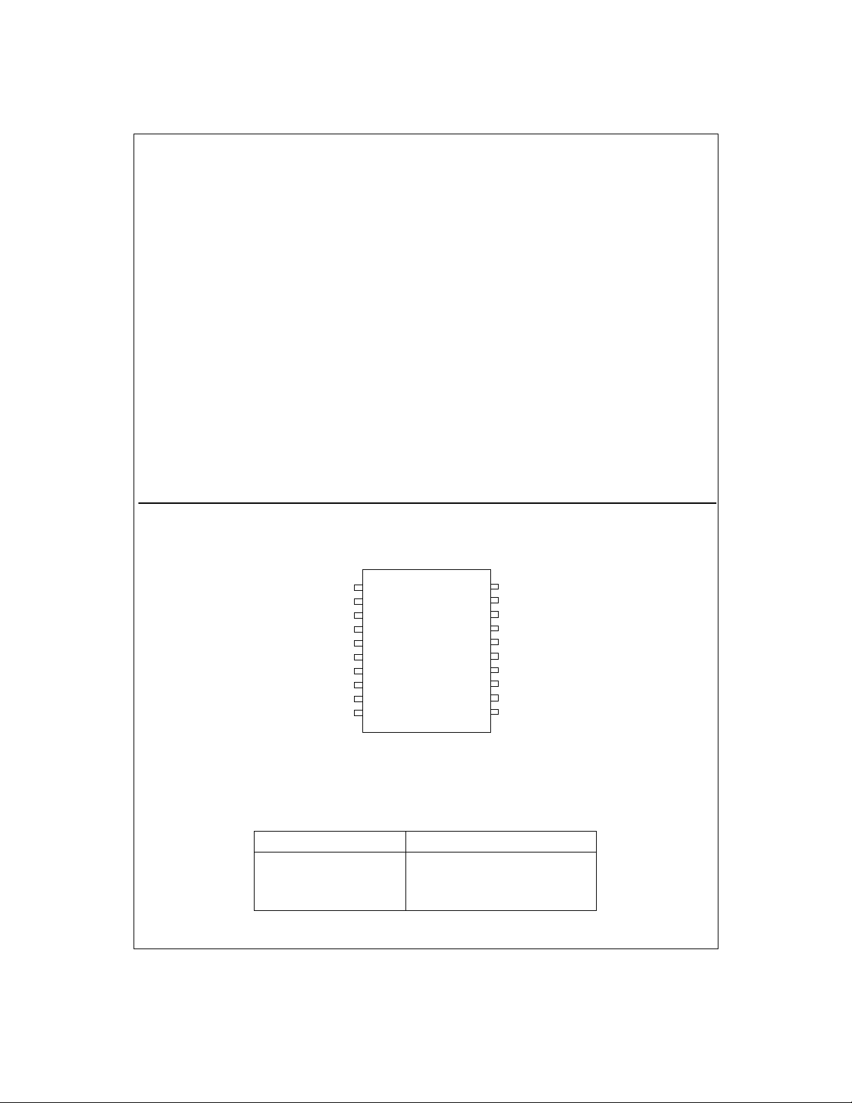
Connection Diagrams
Features
•
6 million pixels/s conversion rate
•
Digitally programm ed gain and offset for red, green and blue
pixels
•
Correlated Double Sampling for lowest noise
•
TTL/CMOS input/output compatible
Key Specifications
•
Output Data Resolution 10/12 Bits
•
Pixel Conversion Rate 6MHz
•
Supply Voltage 5V±5%
•
Power Dissi pation 300mW
LM9810/20 10/12-Bit Image Sensor Processor Analog Front End
July 1998
V
1
REF-
V
REFMID
RefBypass
SampCLK
V
REF+
OS
OS
OS
AGND
2
3
LM9810
4
5
R
6
G
7
B
VA
8
9
10
LM9820
Ordering Information
Commercial (0°C ≤ TA ≤ +70°C) Package
LM9810CCWM
LM9810CCWMX
LM9820CCWM
LM9820CCWMX
TRI-STATE® is a registered trademark of National Semiconductor Corporation.
©1997,1998 National Semiconductor Corporation
DGND
20
VD
19
MCLK
18
D5
17
D4
&
20 Pin Wide SOIC
20 Pin Wide SOIC, Tape & Reel
20 Pin Wide SOIC
20 Pin Wide SOIC, Tape & Reel
16
15
14
13
12
11
D3
D2 (SCLK)
D1 (Latch)
D0 (SDI)
NewLine
1
http://www.national.com
Page 2
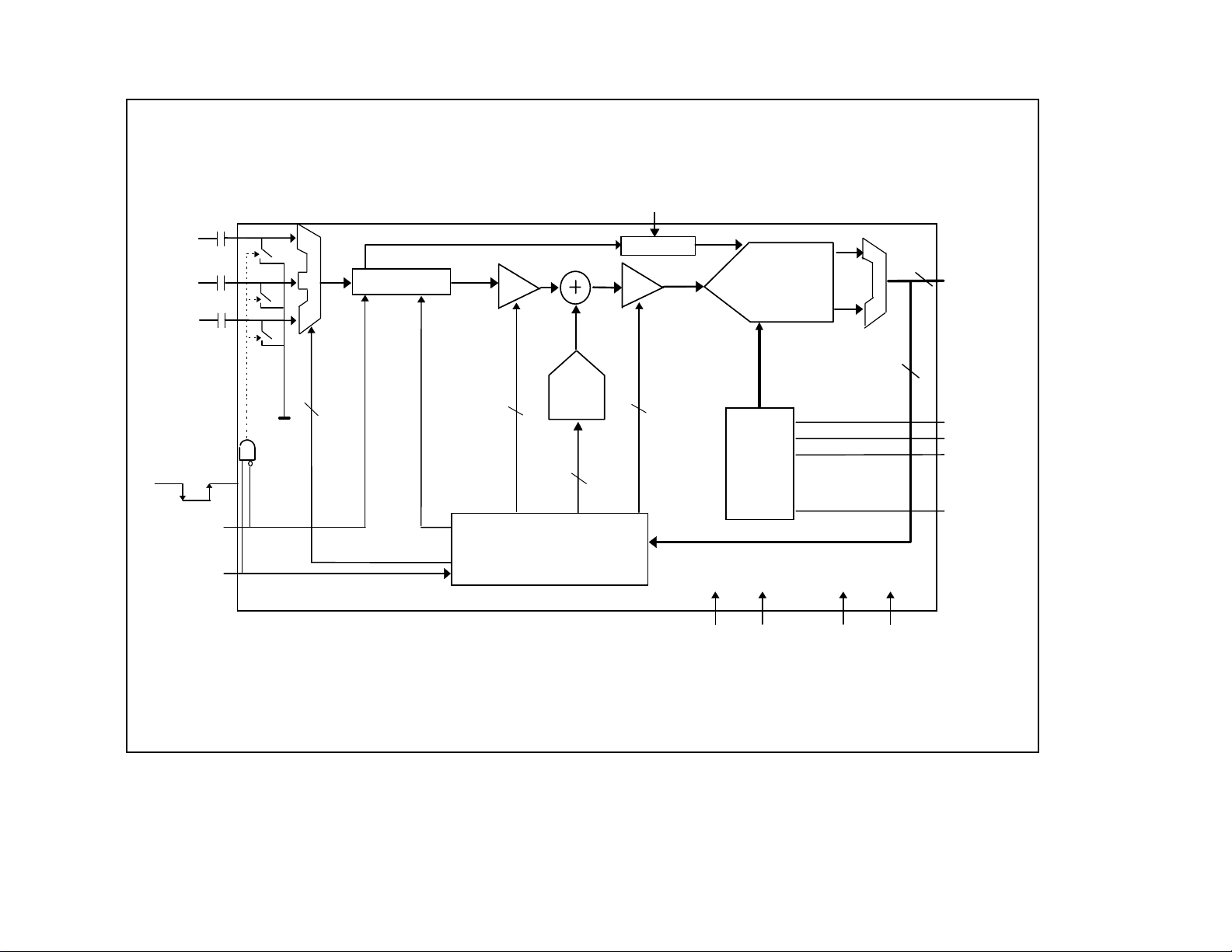
Block Diagram
MCLK
OS
R
OS
G
OS
B
V
signal
V
SampCLK
NewLine
SampCLK
M
U
X
2
V
REF+
or
V
Mux
Select
-
Sampler
0 to 2V
V
Sampling
Mode
SIG
x3 Boost
Gain of
1 or 3
x3
Offset
1
DAC
Offset
6
ADC Clock
PGA
.93 to 3
PGA Gain
5
10/12 bit
6MH z
ADC
Bandgap
Voltage
Reference
M
U
D2,D1,D0
programming
interface
6
D5-D0
3
V
REF+
V
REFMID
V
REF-
RefBypass
Configuration Register
Sampling Mode,
Offset & Gain for R,G,B
VA
AGNDDGND
VD
http://www.national.com
Page 3
(
)
(
)
(
)
Absolute Maximum Ratings
(Notes 1 & 2)
Positive Supply Voltage (V+=VA=VD)
With Respect to GND=
Voltage On Any Input or Output Pin -0.3V to V
Input Current at any pin
Package Input Current
Package Dissipation at T
ESD Susceptibility
AGND=DGND
(Note 3)
(Note 3)
A
(Note 5)
= 25°C
+
±25mA
±50mA
(Note 4)
Human Body Model 2000V
+0.3V
Operating Ratings
Operating Temperature Range T
6.5V
VA
Supply Voltage +4.75V to +5.25V
VD
Supply Voltage +4.75V to +5.25V
VA-VD
|
|
OS
, OSG, OS
R
Input Voltage Range -0.05V to VA + 0.05V
NewLine, SampCLK, D0-D2, MCLK
Input Voltage Range -0.05V to
Soldering Information
Infrared, 10 second s
(Note 6)
300°C
Storage Temperature -65°C to +150°C
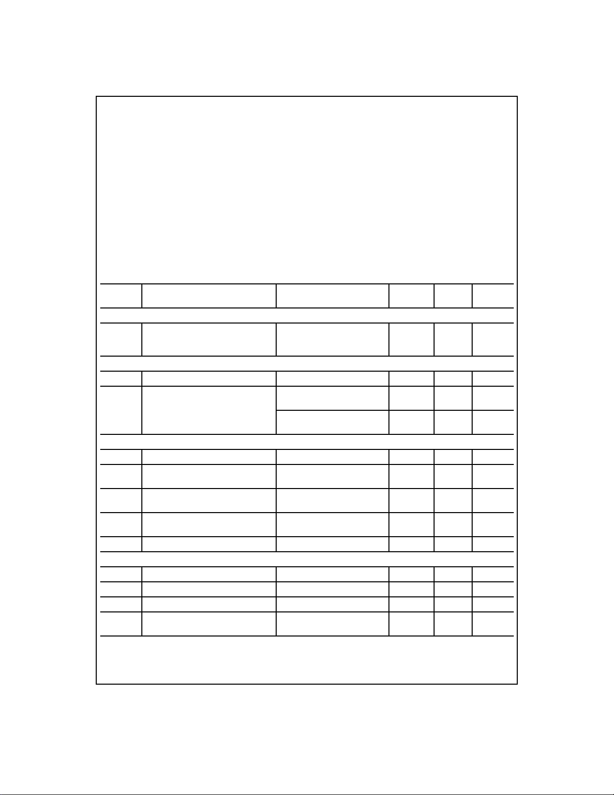
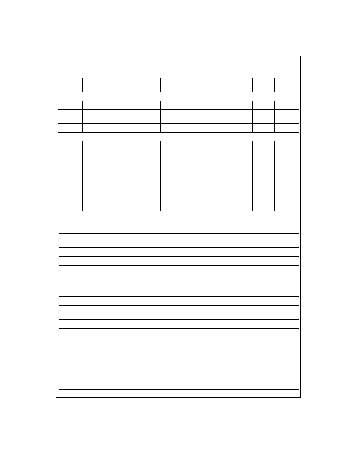
Electrical Characteristics
The following specifications apply for
T
A=TJ=TMIN
to T
; all other limits TA=TJ=25°C.
MAX
AGND=DGND
=0V, VA=VD=+5.0V
(Notes 7, 8, & 12)
Symbol Parameter Conditions
CCD/CIS Source Requirements for Full Specified Accuracy and Dynamic Range
V
OS
Sensor’s Maximum Peak Differential
PEAK
Signal Range
Gain = 0.933
Gain = 3.0
Gain = 9.0
Analog Input Characteristics
OS
OS
OS
,
,
R
Input Capacitance 5 pF
G
B
Measured with OS = 3.5V
OS
OS
OS
,
,
R
Input Leakage Current
G
B
CDS disabled, selected OS input
CDS disabled, unselected OS
input
Coarse Color Balance PGA Characteristics
Monotonicity 5 bits (min)
G
(Minimum PGA Gain) PGA Setting = 0 0.93
0
(Maximum PGA Gain) PGA Setting = 31 3.0
G
31
x3 Boost Gain
Gain Error at any gain
(Note 13)
x3 Boost Setting On
(bit B5 of Gain Register is set)
Internal Reference Characteristics
V
REFMID
V
V
∆
Mid Supply Output Voltage 2.5 V
Positive Reference Output Voltage 3.5 V
REF+
Negative Reference Output Voltage 1.5 V
REF-
Differential Reference Voltage
V
REF
V
- V
REF+
REF-
, f
=24MHz, Rs=25Ω. Boldface limits apply for
DC
MCLK
B
DC
Note 12
(Notes 1 & 2)
≤
Typical
Note 9
MIN
=0°C≤T
Limits
Note 10
T
=+70°C
A
MAX
≤
100mV
VD
+ 0.05V
Units
(Limits)
2.1
0.65
0.21
20 25 µA (max)
10 nA
3.0
.90
.96
2.96
3.15
2.93
3.05
V/V (min)
V/V (max)
V/V (min)
V/V (max)
V/V (min)
V/V (max)
±0.4 1.67 % (max)
2.0 V
V
V
V
3
http://www.national.com
Page 4
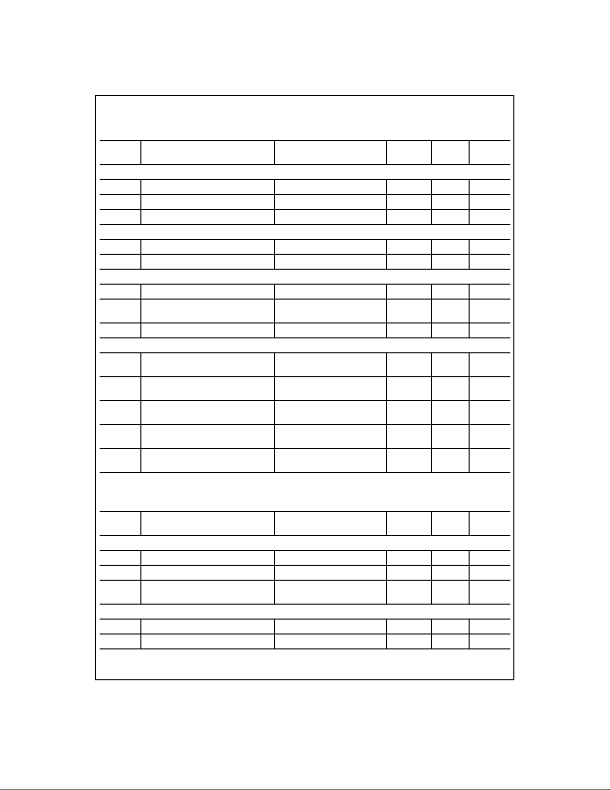
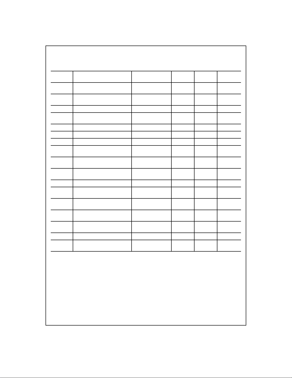
LM9810 Electrical Characteristics
(
)
(
)
(
)
(
)
(
)
(
)
The following specifications apply for
T
A=TJ=TMIN
to T
; all other limits TA=TJ=25°C. All LSB limits are in units of the LM9810’s 10 bit ADC.
MAX
AGND=DGND
=0V, VA=VD=+5.0V
Symbol Parameter Conditions
ADC Characteristics
Resolution with No Missing Codes 10 bits (min)
INL Integral Non-Linearity Error
(Note 11)
DNL Differential Non-Linearity ±0.25 ±1.0 LSB (max)
Full Channel Linearity
INL Integral Non-Linearity Error
Note 14
(Note 11)
DNL Differential Non-Linearity ±0.40 LSB
Static Offset DAC Characteristics
Monotonicity 6 bits (min)
Offset DAC LSB size PGA gain = 1 5
Offset DAC Adjustment Range PGA gain = 1 ±150 ±140 LSB (min)
System Characteristics (see section 1.7.1, Internal Offsets)
Analog Channel Gain Constant
C
(ADC Codes/V)
V
V
V
V
Pre-Boost Analog Channel Offset Error,
OS1
CCD Mode
Pre-Boost Analog Channel Offset Error,
OS1
CIS Mode
Pre-PGA Analog Channel Offset Error -10
OS2
Post-PGA Analog Channel Offset Error -11
OS3
Includes voltage reference
variation, gain setting = 1
, f
=24MHz, Rs=25Ω. Boldface limits apply for
DC
MCLK
(Notes 7, 8, & 12)
Typical
Note 9
±0.35 ±1.5 LSB (max)
±0.9 LSB
502
4.4
4.5
Limits
Note 10
3.4
6.4
468
532
-7.2
+15.7
-6.5
+15.2
-28
+5.3
-30.6
+7.3
LSB (min)
LSB (max)
LSB (min)
LSB (max)
LSB (min)
LSB (max)
LSB (min)
LSB (max)
LSB (min)
LSB (max)
LSB (min)
LSB (max)
Units
(Limits)
LM9820 Electrical Characteristics
The following specifications apply for
T
A=TJ=TMIN
to T
; all other limits TA=TJ=25°C. All LSB limits are in units of the LM9820’s 12 bit ADC.
MAX
AGND=DGND
=0V, VA=VD=+5.0V
Symbol Parameter Conditions
ADC Characteristics
Resolution with No Missing Codes 12 bits (min)
INL Integral Non-Linearity Error
(Note 11)
DNL Differential Non-Linearity ±0.6
Full Channel Linearity
INL Integral Non-Linearity Error
Note 14
(Note 11)
DNL Differential Non-Linearity ±0.65 LSB
, f
=24MHz, Rs=25Ω. Boldface limits apply for
DC
MCLK
(Notes 7, 8, & 12)
Typical
Note 9
Limits
Note 10
±1.1 ±4.0 LSB (max)
+1.75
-1.0
±3.4 LSB
4
http://www.national.com
Units
(Limits)
LSB (max)
Page 5
(
)
(
)
(
)
(
)
)
)
)
)
LM9820 Electrical Characteristics
The following specifications apply for
T
A=TJ=TMIN
to T
; all other limits TA=TJ=25°C. All LSB limits are in units of the LM9820’s 12 bit ADC.
MAX
AGND=DGND
(Continued)
=0V, VA=VD=+5.0V
,
f
DC
MCLK
Symbol Parameter Conditions
Static Offset DAC Characteristics
Monotonicity
Offset DAC LSB size PGA gain = 1 20
Offset DAC Adjustment Range PGA gain = 1 ±590
System Characteristics (see section 1.7.1, Internal Offsets)
Analog Channel Gain Constant
C
(ADC Codes/V)
V
V
V
V
Pre-Boost Analog Channel Offset Error,
OS1
CCD Mode
Pre-Boost Analog Channel Offset Error,
OS1
CIS Mode
Pre-PGA Analog Channel Offset Error -40
OS2
Post-PGA Analog Channel Offset Error -44
OS3
Includes voltage reference
variation, gain setting = 1
DC and Logic Electrical Characteristics
The following specifications apply for
T
A=TJ=TMIN
to T
; all other limits TA=TJ=25°C.
MAX
AGND=DGND
=0V, VA=VD=+5.0V
(Notes 7 & 8)
Symbol Parameter Conditions
D0-D2, MCLK, NewLine, SampCLK Digital Input Characteristics
V
V
C
Logical “1” Input Voltage
IN(1
Logical “0” Input Voltage
IN(0
I
Input Leakage Current
IN
Input Capacitance 5 pF
IN
VD
VD
V
IN
VIN=
=5.25V
=4.75V
=
D0-D5 Digital Output Characteristics
VD
V
V
OUT(1
OUT(0
I
OUT
Logical “1” Output Voltage
Logical “0” Output Voltage
TRI-STATE® Output Current
D0-D5
(
only)
=4.75V, I
VD
=4.75V, I
VD
=5.25V, I
V
OUT
V
OUT
Power Supply Characteristics
Operating
Analog Supply Current
I
A
Standby with input clocks stopped
Standby with input clocks running
Operating
Digital Supply Current
I
D
(Note 15)
Standby with input clocks stopped
Standby with input clocks running
VD
DGND
DGND
=
VD
=
DC
OUT
OUT
OUT
,
f
MCLK
=-360µA
=-10µA
=1.6mA
=24MHz, Rs=25Ω.
=24MHz, Rs=25Ω.
Boldface limits apply for
(Notes 7, 8, & 12)
Typical
Note 9
Limits
Note 10
6
14
26
±575
2008
17.6
18
1873
2129
-32.1
+68.9
-22.2
+57
-94.3
+16.4
-121
+28
Boldface limits apply for
Typical
Note 9
Limits
Note 10
2.0
0.8
0.1
-0.1
2.4
4.4
0.4
0.1
-0.1
45
0.8
57
0.9
3.0
220
110
320
200
220
Units
(Limits)
bits (min)
LSB (min)
LSB (max)
LSB (min)
LSB (min)
LSB (max)
LSB (min)
LSB (max)
LSB (min)
LSB (max)
LSB (min)
LSB (max)
LSB (min)
LSB (max)
Units
(Limits)
V (max)
V (min)
µA(max)
µA(max)
V (min)
V (min)
V (max)
µA
µA
mA (max)
mA (max)
mA
µA (max)
µA (max)
µA
5
http://www.national.com
Page 6
AC Electrical Characteristics
The following specifications apply for
limits apply for T
A=TJ=TMIN
Symbol Parameter Conditions
AGND=DGND
to T
; all other limits TA=TJ=25°C.
MAX
=0V, VA=VD=+5.0V
(Notes 7 & 8)
=24MHz
,
t
MCLK
Typical
(Note 9)
=1/f
CLK
M
,
=5ns, Rs=25Ω.
t
r=tf
Limits
(Note 10)
,
f
DC
MCLK
Boldface
Units
(Limits)
f
MCLK
t
MCLK
t
SCNL
t
SampCLK
t
SampLo
t
SampHi
t
SampSU
t
DDO
t
HDO
t
SCLK
t
DSU
t
DH
t
SCLKLA
t
LASCLK
t
LA
t
LANL
Maximum
MCLK
MCLK
SampCLK
MCLK
Frequency
Duty Cycle
period 41 ns (min)
falling edge before
NewLine
falling edge
SampCLK
period
Low time for
High time for
SampCLK
edge of
falling edge of
SampCLK
SampCLK
falling edge before rising
MCLK
MCLK
before new valid
50 ns (min)
50 ns (min)
data
hold time of current data from falling
MCLK
edge of
D2
(SCLK) Serial Clock Period 1 t
Input data setup time before
D2
(SCLK) rising edge
Input data hold time after D2(SCLK)
rising edge
D2
(SCLK) rising edge after bit B0
D1
before
(Latch) rising edge
D1
(Latch) rising edge before next
D2
(SCLK) rising edge
High time for D1(Latch)
D1
(Latch) rising edge before
NewLine
falling edge
24
40
60
3
4
4
40
15
0
3
3
3
3
3
MHz (min)
% (min)
% (max)
t
(min)
MCLK
t
(min)
MCLK
ns (min)
ns (max)
ns (min)
(min)
MCLK
ns (min)
ns (min)
ns (min)
ns (min)
t
(min)
MCLK
t
SampCLK
(min)
Note 1: Absolute Max im um R atings indicate limits beyond wh ic h damage to the device may occur. Operating R atings indicate condit ions for which the device is functional,
but do not guarantee specific perfor m ance limits. For guaranteed specifications an d test conditions, see the Electrical C haracteristics. The guaranteed specifications apply
only for the test condition s lis te d. Some performance ch arac t eristics may degrade when th e devi ce is not operated under the listed te s t conditions.
Note 2: All voltages are measured with respect to GND=
Note 3: When the input voltage (V
maximum package inp ut c urrent rating limits the num ber of pins that can simultan eously safely exceed the power suppli es w it h an input current of 25mA t o two.
Note 4: The maximum power dissipation must be derated at elevated temperatures and is dictated by T
able power dissipation at any temperature is P
is 84°C/W for the M20B SOI C package
Note 5: Human body m odel, 100pF capacit or discharged through a 1. 5kΩ resistor.
Note 6: See AN450 “Surface M ount ing M et hods and T heir Effect o n Prod uct Re liabilit y” o r the sect ion ti tled “ Surface M oun t” found in any N ation al Se mic ondu cto r Linea r
Data Book for other methods of soldering surface mount devices.
) at any pin exceed s the p ower su ppl ies (VIN<GND or VIN>VA or VD), the current at that pin sho uld be limite d to 25mA . The 50mA
IN
.
AGND=DGND
= (TJmax - TA) / ΘJA. TJmax = 150°C for this device. The typical thermal resistance (ΘJA) of this part when board moun te d
D
=0V, unless otherwise specified.
6
max, ΘJA and the ambient temperatu re, TA. The maximum a llow -
J
http://www.national.com
Page 7
Note 7: Two diodes clamp the OS analo g inputs to
impedance of the sens or, prevents damage to the LM9810/2 0 f rom t ransients during power-u p.
AGND
and VA as shown below. This input protection, in co m bination with the external clamp capa c it or and the output
VA
OS Input
TO INTERNAL
CIRCUITRY
AGND
Note 8: To guarantee accuracy, it is required that VA and VD be connected together to the same power supply with separate bypass capacitors at each supply pin.
Note 9: Typicals are at T
J=TA
=25°C, f
= 24MHz, and repre s ent most likely parametric norm.
MCLK
Note 10: Tested limits are guaranteed to Nat ional's AOQL (Average Outgoing Quali ty Level).
Note 11: Integral non-linearity error is defined as the deviation of the analog value, expressed in LSBs, from the straight line th at best fits the actual transfer function of the
ADC.
Note 12: V
a white (full scale) image with respect to the reference level, V
correctable range of pixel-to-pixel V
LM9810/20 can corr ec t for using its internal PGA .
Note 13: PGA Gain Error is the maximum difference between the measured gain for any PGA code and the ideal gain calculated by using the formula
Gain
is defined as the CCD OS voltage for the reference period f ollowing the reset feedthrough pulse. V
PGA
REF
V
--- -
V
variation is define d as the maximu m variation in V
WHITE
PGA code
G0X
where .
-------------- ------------ -+=XG
32
31G0
.
REF
32
–()
------=
31
V
is defined as the peak positive deviation above V
RFT
CCD Output Signal
V
RFT
V
V
REF
WHITE
(due to PRNU, light source intensity variation, optics, etc.) that the
WHITE
is defined as the peak CCD pixel output voltage for
WHITE
of the reset feedthrough pulse. The maximum
REF
Note 14: Full C hannel INL and DNL are tested with CDS disabled, negative signal polarity, and a single OS input with a gain register setting of 1 (000001b) and an offset
register setting of 0 (000000b).
Note 15: The digital supply current (I
The current required to switch the digital data bus can be calculated from: Isw = 2*Nd*Psw*CL*
of each data bit switchin g, C L is t he capacitive loading on each data pin,
6, Psw should be .5, and
ital output pin (
will be drawn through the
VD
D5
- D0) is 20pF and the period of tSampCLK is 1/6MHz or 167ns , then the digital switching current would be 7.2mA. The calculated digital switching current
VD
) does not include the load, data and switching frequency dependent current required to drive the digital output bus on pins (D5 - D0).
D
VD
is the digital suppl y volta ge and tSampCLK i s the period of the
VD
/tSampCLK where N d is total number of data pins, Psw is the probability
SampCLK
signal. Since Nd is
is nominally 5V, the switching current can usually be calculated from: Isw = 30*CL/tSampCLK. For example, if the capacitive load on each dig-
pin and should be con s idered as part of the total power budget for he LM9810/20.
7
http://www.national.com
Page 8

Pin Descriptions
Analog Power
VA
AGND
OS
OS
,
R
RefBypass
V
REF+
,
V
REF-
MCLK
SampCLK
NewLine
G
V
REFMID
This is th e po si t ive supply p i n f o r t h e an al og
supply. It should be connected to a voltage
source of +5V and bypassed to
0.1µF monolithic capacitor in parallel with a
10µF tantalum capacitor.
This is the ground return for the analog supply.
OS
,
, Analog Inputs. These inputs (for Red,
B
Green, and Blue) should be tied to the sensor’s OS (Output Signal) through DC blocking capacitors.
Internally generated reference voltage
bypass pin. It should be bypassed to
through a .05uF monolithic capacitor.
Voltage reference bypass pins. They should
,
each be bypassed to
monolithic capacitor.
Input & Timing Control
Master Clock. The ADC conversion rate will
be a maximum of ¼ of
24MHz.
Sample Clock.
version rate of the ADC (up to ¼ of the
MCLK
rate) and sample timing. The signal
level is sampled while
held on the rising edge of
CDS is enabled, the falling edge of
causes the CCD reference level to be held.
If CDS is not enabled,
on the falling edge of
on the programmed signal polarity.
is also used with
nal coupling capacitors.
New Line signal. Used to indicate the start
of active pixels on a new line, to allow
clamping of the AC coupling caps, and to
allow programming of the configuration register. When
low, the OS inputs will be connected to
either
MCLK
of
mux and the offset and gain settings will be
set to the appropriate values for the first
color of the next line set in the color mode
setting in the Sampler and Color Mode Register. When
the pixel conversion data from the ADC.
When
STATE and
interface for programming the configuration
registers.
Analog I/O
SampCLK
NewLine
NewLine
is high and
V
V
or
REF+
after
NewLine
. On the first rising edge
REF-
NewLine
goes low, the internal
NewLine
is low, D[5-0] transmit
is high, D[5-0] enter TRI-
D2, D1
and D0 act as a serial
AGND
AGND
through a .05uF
MCLK
. Nominally
controls the con-
SampCLK
is low and
SampCLK
SampCLK
V
V
or
REF+
SampCLK
REF-
, depending
SampCLK
to clamp the exter-
SampCLK
with a
AGND
. When
is held
is
Digital Power
VD
This is the positive supply pin for the digital
supply. It should be connected to a voltage
source of +5V and bypassed to
DGND
0.1µF monolithic capacitor.
DGND
This is the ground return for the digital supply.
Digital I/O
D5-D0
Data Input/Output pins. When
NewLine
low, the 10 or 12 bit conversion results of
the ADC are multiplexed to
NewLine
is high, the output drivers enter TRI-
STATE and
D2, D1
D5-D0
. When
& D0 act as a serial interface for writing to the configuration registers.
LM9810
MCLK0, MCLK1, MCLK2, MCLK3
Output Mode
NewLine
(
Low)
D5
D4
D3
D2
D1
D0
LM9820
b9, b9, b3, b3
b8, b8, b2, b2
b7, b7, b1, b1
b6, b6, b0, b0
b5, b5, 0, 0
b4, b4, 0, 0
MCLK0, MCLK1, MCLK2, MCLK3
Output Mode
NewLine
(
Low)
D5
D4
D3
D2
D1
D0
b11, b11, b5, b5
b10, b10, b4, b4
b9, b9, b3, b3
b8, b8, b2, b2
b7, b7, b1, b1
b6, b6, b0, b0
Input Mode
NewLine
(
High)
D5-D3
D2
(SCLK) Serial Data Clock.
D1
(Latch) Latch and shift enable signal. When
Don’t Care
D1
(Latch) is low, da ta is shifted into D0(SDI).
D1
When
(Latch) go es hi gh , the la st n ine bit s
shifted into
D0
(SDI) will be used to program
the addres sed configuration register. To
avoid erroneous writes to the configuration
D1
registers,
when
D0
(SDI) Serial input data. Data is valid on D2(SCLK)
(Latch) should be pulled low
NewLine
is high.
rising edge. Three address bits followed by
six data bits (MSB first) should be shifted
D0
into
before D1(Latch) goes high.
with a
is
8
http://www.national.com
Page 9

Timing Diagrams
g
Diagram 2:
ram 3:
Dia
Diagram 1:
Pixel Conversion Timing and Latency
and Output Data Timing (
SampCLK
Timing for Programming the Con figuration Registers
NewLine
low)
9
http://www.national.com
Page 10

Timing Diagrams
g
NewLine
RS
OS
Clamp Signal
(Internal)
SampCLK
Ø1
(Even/Odd Mode)
Ø2
(Even/Odd Mode)
Ø1
(Standard Mode)
Ø2
(Standard Mode)
CCD Reset
signal
OS
Optical Black Pixel
Clamp On
Dia
CLAMP OFF
CCD Clamping Timing
ram 4:
Optical Black Pixel
First Active Pixel
SampCLK
Diagram 5:
CDS Timing
10
http://www.national.com
Page 11

Table 1: Configuration Register Address Table
Address
(Decimal)
0000
1001
2010
3011
4100
5101
6110
7111
Address
(Binary)
A2 A1 A0 B5 B4 B3 B3 B2 B1
Data Bits
Sampler and Color Mode
CDS Polarity N/A Mode2 Mode1 Mode0
Red DAC Offset Setting
Polarity MSB LSB
Green DAC Offset Setting
Polarity MSB LSB
Blue DAC Offset Setting
Polarity MSB LSB
Red Gain Setting
x3 MSB LSB
Green Gain Setting
x3 MSB LSB
Blue Gain Setting
x3 MSB LSB
Production Test and Pow er Down
Test Test T est Test Test PD
11
http://www.national.com
Page 12

Table 2: Configuration Register Parameters
Parameter
(Address)
CDS Enable
(0)
Signal Polarity
(0)
Color Mode
(0)
Control Bits Result
Sampler and Color Mode (0)
B5
0
1
B4
0
1
B2 B1 B0
Line Rate Color -
000
* state of the first line after a write to this register
001
010
011
100
101
110
Single Input Color - Mux selects
pixel rate:
RESERVED
Monochrome Mux selects
Monochrome Mux selects
Monochrome Mux selects
Bayer - Mux selects
* state of the first line after a write to this register
CDS Enabled
Single Ended (CDS disabled)
Negative Polarity
Positive Polarity
Mux, Gain & Offset change at the line rate:
*1st line: Mux =
2nd line: Mux =
3rd line: Mux =
OS
, Gain & Offset = R
R
OS
Gain & Offset = G
G
OS
Gain & Offset = B
B
repeat…
OS
input. Gain & Offs e t change at the
B
Gain & Offset = R,G,B,R,G,B…
OS
input. Gain & Offset = R
R
OS
input. Gain & Offset = G
G
OS
input. Gain & O ffset = B
B
OS
input. Gain & Offset change at the pixel rate:
B
*1st line: Gain & Offset = G,R,G,R,...
2nd line: Gain & Offset = B,G,B,G,…
repeat…
Green Stripe - Mux selects
rate:
111
* state of the first line after a write to this register
OS
input. Gain & Offset change at the pixel
B
*1st line: Gain & Offset = R,G,B,G,R,G,B,...
2nd line: Gain & Offset = B,G,R,G,B,G,R,…
repeat…
12
http://www.national.com
Page 13

(
)B4(
)
(
)
yp
)
(
yp
Table 2: Configuration Register Parameters
(Continued)
Parameter
(Address)
Offset Polarity
(1,2 & 3)
Offset Value
1,2 & 3
Typical Offset
Values
1,2 & 3
Boost Gain
Enable
(4,5 & 6)
Control Bits Result
Red, Green and Blue Offset DAC Settings (1, 2 & 3)
B5
0
1
MSB)B3 B2 B1 B0(LSB
B5
(SIGN)
0
0
0
• • •
0
0
1
1
1
• • •
1
1
B4
(MSB)
0
0
0
• • •
1
1
0
0
0
• • •
1
1
B3
0
0
0
• • •
1
1
0
0
0
• • •
1
1
B2
0
0
0
• • •
1
1
0
0
0
• • •
1
1
Positive Offset
Negative Offset
LM9810: Offset = 5LSBs * Offset Value * PGA Gain
LM9820: Offset = 20LSBs * Offset Value * PGA Gain
B1
0
0
1
• • •
1
1
0
0
1
• • •
1
1
B0
(LSB)
0
1
0
• • •
0
1
0
1
0
• • •
0
1
Red, Green and Blue Gain Settings (4,5 & 6)
B5
0
1
Boost Gain = 1V/V
Boost Gain = 3V/V
ical Offset (with PGA Gain = 1
T
LM9810 LSBs
0.00
+5
+10
• • •
+150
+155
0
-5
-10
• • •
-150
-155
LM9820 LSBs
0.00
+20
+40
• • •
+600
+620
0
-20
-40
• • •
-600
-620
PGA Gain Value
(4,5 & 6)
Gain
(4,5 & 6)
Typical Gain
Values
(4, 5 & 6)
B4
B5
x3)
• • •
• • •
• • •
B3
B4
(MSB)
0
0
0
0
0
0
1
1
1
1
1
1
0
0
0
• • •
1
1
1
• • •
0
0
0
• • •
1
1
1
B2 B1 B0
B3
0
0
0
• • •
1
1
1
• • •
0
0
0
• • •
1
1
1
Gain = Boost Gain * PGA Gain
B2
0
0
0
• • •
1
1
1
• • •
0
0
0
• • •
1
1
1
13
PGA Gain (V/V) =.933 + 0.0667 * (PGA Gain Value)
B1
0
0
1
• • •
0
1
1
• • •
0
0
1
• • •
0
1
1
B0
(LSB)
0
1
0
• • •
1
0
1
• • •
0
1
0
• • •
1
0
1
T
ical Gain
(V/V)
0.93
1.00
1.13
• • •
2.87
2.93
3.00
• • •
2.79
3.00
3.20
• • •
8.60
8.80
9.00
http://www.national.com
Page 14

p
Table 2: Configuration Register Parameters
(Continued)
Parameter
(Address)
Production Te st
(7)
Power Down
Enable
(7)
B5
B0
Control Bits Result
Production Test and Power Down (7)
B4
0
1
B3 B2 B1 Should all be set to zero for normal o
Normal Operation
Power Down
eration
14
http://www.national.com
Page 15

Applications Informati on
g
g
p
g
1.0 Programming the LM9810/20
1.1 Writing to the Configuration Register
NewLine
When
ing to the configuration registers.
(SCLK),
shift enable signal (Latc h). When
shifted into
D2
(SCLK). Three reg ister address bits followed by six data bits
should be shifted into
tions from low to high, the last 6 data bits will be stored into the
configuration registe r addressed by the previous 3 address bits
(as shown in Diagram 3).
3 cycles of the serial clock on
tion register.
1.2 CDS Mode
The LM9810/20 uses a high-p erforman ce CDS (Corr elated D ouble Sampling) circuit to re move many sources of noise a nd error
from the CCD signal. It also suppor ts CIS image sensors wit h a
single sampling mode.
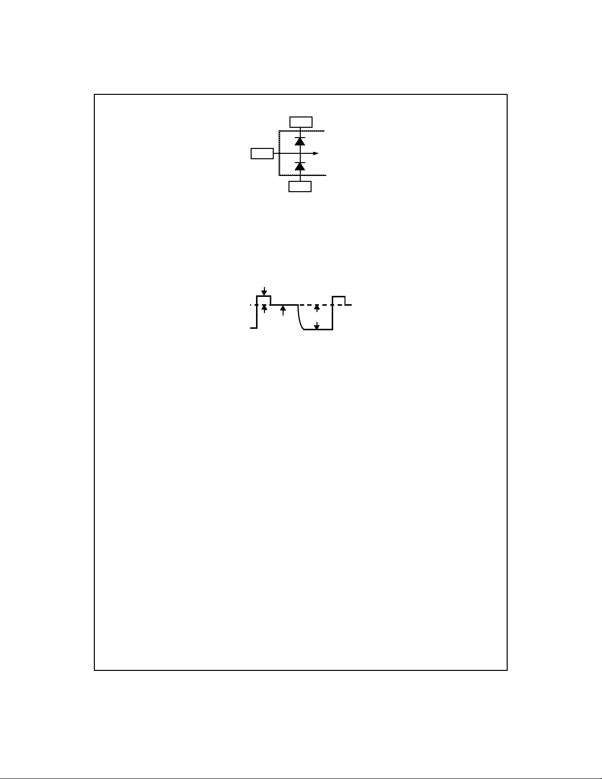
Figure 1 shows the output stage of a typical CCD and the resulting output waveform:
RS (RESET)
SampCLK
Capacitor C1 converts the electrons coming from the CCD’s shift
register to an analog voltage. Th e source follower output stage
(Q2) buffers this voltage before it le aves the CCD. Q1 resets the
voltage across capacitor C1 betwee n pixels at intervals 2 and 5 .
When Q1 is on, th e out put sign al (OS) i s a t its most positive voltage. After Q1 tur ns off (period 3), the O S level represents the
residual voltage across C1 (V
charge injection from Q1 , thermal no ise from the ON r esistance
of Q1, and other sources of erro r. When the shift register clock
(Ø1) makes a low to high transition (period 4), the electrons from
the next pixel flow into C1. The charge across C1 now contains
the voltage proporti onal to the number of ele ctrons plus V
, an error term. If OS is sa mpled at the end of peri od 3 and
UAL
that voltage is subtracted from the OS at the end of per iod 4, the
V
RESIDUAL
is high, D2, D1 & D0 act as a serial interface for writ-
D2
D0
is the input data pin (SDI), and D1 is the latch and
D0
(SDI), and must be valid on each rising edge o f
D0
(SDI),
D1
(Latch) must remain h igh for at leas t
is the input serial clock
D1
(Latch) is low, serial data is
MSB first. When D1(Latch) transi-
D2
(SCLK) to write to the confi g ura-
V
DD
Q1
C1
e-
(from shift register)
Q2
OS
V
SS
Ø1
RS
OS
123 4 5
ure 1: CDS
Fi
RESIDUAL
). V
RESIDUAL
includes
RESID-
term is canceled and the noise on the signal is
reduced ([V
principal of Correlated Double Sampling.
SIGNAL+VRESIDUAL
]-V
RESIDUAL
= V
SIGNAL
). This is the
If the LM9810/20 is programmed for corr elated double samp ling
(bit B5 of register 0 is cleared), then the falling edge of
SampCLK
should occur toward the end of per iod 3 and the rising edge of
SampCLK
should occur towards the e nd of per iod 4. While
CLK
is high, the Reference level (V
held at the falling edge of
nal level (V
ing edge of
+ V
SIGNAL
RESIDUAL
SampCLK
. The output from the sampler is the potential
RESIDUAL
SampCLK
. While
) is sampled and it is held at the ris-
difference between the two samples, or V
) is sampled, and it is
SampCLK
.
SIGNAL
Samp-
is low, the sig-
1.3 CIS Mode
The LM9810/20 supports CIS (Contact Image Sensor) devices by
offering a sampling mode for capturing positive going signals, as
opposed to the CCD’s negative going signal. The output signal of
a CIS sensor (Figure 2) differs from a CCD signal in two primary
ways: its output increases with increasing si gnal strength, and it
does not usually have a reference level as an integral par t of the
output waveform of every pixel.
OS (CIS)
OS (CCD)
123 4 5
SampCLK
CIS
ure 2:
Fi
When the LM9810/ 20 is in CIS mode (Regist er 0, B5 =1), it u ses
V
V
or
either
REF+
of the Sampling and Color Mode register) as the reference (or
depending on th e signal p olari ty setting (B4
REF-
black) voltage for each pixel. If the signal polarity is set to one,
V
then
signal will be held on the rising edge of
zero, then
the OS signal will be held on the rising edge of
ing edge of
will be held on the falling edge of
REF-
V
will be held on the falling edge of
REF+
SampCLK
should occur near the e nd of per iod 4, and
at least 50ns after the falling edge of
1.4 Multi
lexer/Channel Switchin
SampCLK
SampCLK
SampCLK
SampCLK
.
and the OS
. If it is set to
SampCLK
and
. The ris-
The offset and gain sett ings auto matical ly switch after each ADC
conversion according to the color mode setting in th e Sampler
and Color Mod e register (register 0). For example, if the color
mode (bits B2,B1 & B0) is set to 001, the offset and gain will alternately switch between the R, G and B settings after each conversion. The input multiplexer never changes durin g a line, but if the
color mode is set to Line Rate Color (000), the mux will automatically switch after each new line.
The offset and gain settings will always start with the first channel
of the programmed mode after a falling edge on
NewLine
. For
15
http://www.national.com
Page 16

example, the R offset and gain settings will be used for the first
g
g
q
q
q
q
q
conversion following a falling edge on
NewLine
if the color mode is
set to Single Input Color (001).
For the Single Input Co lor, Bayer and Green Stripe mod es, the
mux will always connect the
and gain settings will alternate values every pixel according to the
OS
input to the sampler. The offset
B
order indicated by the Sampler and Color Mode register (see
Table 2). T he first falling edge of
NewLine
following a write to the
Sampler and Color Mode register will ready the offset and gain to
cycle through the colors o f the first lin e of the p rogrammed color
mode. Each subsequent falling edge of
NewLine
will switch the offset and gain settings to the first color of the next line. The
LM9810/20’s unused OS inputs should not be left uncon nected.
All three OS inputs should be tied together on the LM9810/20
side of the clamp capacitor (see Figure 3).
C
SENSOR
DOS
CLAMP
OS
NC
OS
OS
OS
B
G
R
1.7 Offset DAC
The Offset DAC removes the DC offsets generated by the sensor
and the LM9810/20’s analog signal chain (see section 1.7.1,
Internal Offsets). The DAC value for each color (registers 1,2 and
3) should be set during calibration to the lowest value that still
results in an ADC output code greater than zero for all the pixels
when scanning a black line. With a PGA gain of 1V/V, each LSB
of the offset DAC typically adds the equivalent of 5 LM9810 LSBs
or 20 LM9820 LSBs, providing a total offset adjustment range of
±150 LM9810 LSBs or ±590 LM9820 LSBs. The Offset DAC’s
output voltage is given by:
V
DAC
E
uation 2:
⋅=
9.75mV (value in B4 - B0)
Offset DAC Output Voltage
In terms of output codes, the offset is given by:
Offset 5LSBs (value in B4 - B0) PGA Gain
E
uation 3:
Offset 20LSBs (value in B4 - B0) PGA Gain
E
uation 4:
⋅⋅=
LM9810 Offset Equation
⋅⋅=
LM9820 Offset Equation
LM9810/20
Figure 3:
For the Line Rate Color mode, the mux will cycle through the
OS
and
G
and B offset & gain settings will be used when the mux is set to
OS
the
gain settings will always be used on the first line following a write
OS Connections for single output sensors
OS
inputs after each falling edge of
B
OS
and
G
OS
input, respectively.
B
,
R
NewLine
. The R, G
OS
and the R offset &
R
OS
register 0.
1.5 Data Latency
SampCLK
The latency through the LM9 810/20 is 8
MCLK
one
period. The data o utput on D5 - D0 (MSBs b11 - b6 or
periods plus
b9 - b4) represents data whose reference sig nal was sampled 8
SampCLK
t
1.6 Pro
MCLK
+ t
SampSU
+ t
rammable Gain
earlier (see Diagram 1).
The output of the Sampler drives the input of the x3 Boost gain
stage. The gain of the x3 Boost g ain is 3V/V if bit B 5 of the current color’s gain register (registers 4,5, and 6) is set, or 1V/V if bit
B5 is cleared. The output o f the x3 gain stage is the i nput to the
offset DAC and the output of the offset DAC is the input to the
PGA (Programmable Gain Am pli fie r). The PGA provides 5 b its o f
gain correction over a 0.93V/V to 3V/V (-0.6 to 9.5dB) range. The
x3 Boost gain stage and the P GA can be co mbin ed for an overall
gain range of .93V/V t o 9.0V/V (-.6 to 19dB ). The ga in set ting for
each color (registers 4 , 5 and 6) should be se t during calibration
to bring the maximum amp litude of the strongest pi xel to a level
just below the desired maximum output from the ADC. The PGA
gain is determined by the following equation:
V
--- -
PGA Gain
V
0.933 + .0667 (value in bits B4-B0)=
uation 1:
E
PGA Gain
If the x3 Boost gain is enabled then the overall signal gain will be
three times the PGA gain.
The offset is positive if bit B5 is clear ed and n egati ve if B5 is set.
Since the analog offs et is added before the PGA gain, the value
of the PGA gain must be consider ed when selecting the offset
DAC values.
,
R
1.7.1 Internal Offsets
Figure 4 is a model of the LM9 810/2 0’s internal of fsets. Equati on
5 shows how to calculate the expected output code given the
input voltage (V
OS3
V
), the programmed offset DAC voltage (V
grammed gains (G
IN
), the LM9810/20 inter nal offsets ( V
B
PGA
, G
) and the analog channel gain con-
DAC
stant C.
C is a constant that combines the gain error through the AFE, reference voltage variance, and ana log voltage to digital co de conversion into one constant. Ideally, C = 2048 codes/V (4096
codes/2V) for the LM98 20 and 512 code s/V (1024 codes/2V) for
the LM9810. Manufacturing tolerances widen the range of C (see
Electrical Specifications).
x3 Boost
1V/V or
3V/V
+
V
Σ
IN
+
V
OS1
=
D
OUT
E
uation 5: Output code calculation with internal offsets
+
G
B
Σ
+
V
OS2
ure 4:
Fi
+()
VINV
OS1
PGA
0.93V/V to
3V/V
DAC
+
G
PGA
ADC
Σ
+
V
OS3
+
Σ
+
Offset
DAC
V
Internal Offset Model
++()
G
BVDACVOS2
G
PGAVOS1
Equation 6 is a simplification of the output code calculation,
neglecting the LM9810/20’s internal offsets.
16
http://www.national.com
OS1
OS2
, V
,
), the pro-
D
OUT
+()
C
Page 17

=
g
D
OUTVINGBVDAC
+()
G
PGA
C
Equation 6: Simplified output code calculation
the LM9810/20 is operating in CDS mode. In CDS mode, the
LM9810/20 leakag e current s hould be no more t han 20nA. With
CDS disabled, which will likely be the case when CIS sensors are
used, the LM9810 /20 lea kage cu rrent can be as hi gh as 25uA at
the maximum conversion rate.
1.8 Power Down Mode
Setting the Power Down (bit B0 of register 7) puts the device in a
low power standby mode. The analog sections are turned off to
conserve power. The digital logic will continue to operate if
continues, so for minimum power dissipation
MCLK
MCLK
should be
stopped when the LM9810/20 enters the Power Down mode.
Recovery from Power Down typically takes 50µs (the time
required for the reference voltages to settle to 0.5 LSB accuracy).
2.0 Clamping
To perform a DC restore across the AC coupling capacitors at the
beginning of every line, the LM9810/20 implements a clam ping
NewLine
function. When
is high and
inputs will be connected to either
of the Sampling and Color Mode register. If B4 is set to one (positive signal polarity), then the OS inputs will be connected to
. If B4 is set to zero (negative signal polarity), then they will be
connected to
V
REF+
.
SampCLK
V
REF+
is low, all three OS
V
or
, depending on B4
REF-
V
REF-
2.1 Clamp Capacitor Selection
This section explains how to sel ect appropriate clamp c apacitor
values.
C
CLAMP
OS
OS
SENSOR
DOS
NC
V
REF+
or
V
REF-
LM9810/20
Figure 5:
OS Clamp Capacitor and Internal Clamp
The output signal of many sensors ri des on a DC offset (greater
than 5V for many CCDs) which is incompatible with the
LM9810/20’s 5V operation. To eliminate this offset without resorting to additional higher voltage components, the output of the
sensor is AC coupled to the LM 9810/20 through a DC blocking
capacitor, C
used. The value of this capaci tor is determined by the lea kage
. The sensor’s DOS output, if available, is not
CLAMP
current of the LM9810/20’s OS input and the output impedance of
the sensor. The leakage t hrough the OS input de termines how
quickly the capacitor value will drift from the clamp value of
V
or
, which then deter mines how many pixels can be pro-
REF-
cessed before the droop causes errors in the conversion (±0.1V
V
REF+
is the recommended limit for CDS ope ration). The output impedance of the sensor deter mines how quickly the ca pacitor can be
charged to the clamp value d uring the black reference per iod at
the beginning of every line.
The minimum clamp capacitor value is de termined by th e maximum droop the LM9810/20 can tolerate while converting one
sensor line. The minimum clamp capacitor value is much small er
for CDS mode applications t han it is for CIS mode applicat ions.
The LM9810/20 input lea kage current is conside rably less when
2.1.1 CDS mode Minimum Clamp Capacitor Calculation:
The following equation takes the maximum leakage current into
the OS input, the maximum allowable droop, the number of pixels
on the sensor, and the pixel conversion rate, f
vides the minimum clamp capacitor value:
i
C
CLAMP MIN
Equation 7:
-------- -dt=
dV
leaka
e current (A)
-------------------- ------------------------------ max droop(V)
CDS mode C
CLAMP MIN
number of pixels
----------------- -------------------------- -=
Calculation
SampCLK
f
SampCLK
, and pro-
For example, if the OS input leakage curren t is 20nA wors t-case,
the sensor has 2700 act ive pixels, the conversion rate is 2MHz
(t
mum clamp capacitor value is:
= 500ns), and the max droop desi red is 0.1V, the mini-
SampCLK
2700
20nA
-------------- -=
270pF=
------------- 2MHz
0.1V
CLAMP MIN
C
Equation 8:
CLAMP MIN
CDS mode C
Example
2.1.2 CIS mode Minimum Clamp Capacitor Calculation:
If CDS is disabled, th en the m aximum L M9 810 /20 OS inpu t l e akage current can be calculated from:
=
I
leakageVSATfSampCLKCSAMP
Equation 9:
where V
and C
CIS mode Input Leakage Current Calculation
SAT
is the peak pixel signal swing of the CIS OS output
SAMP
is the capacitance o f the LM9810/ 20’s internal sam-
pling capacitor (2pF). Inserting this into Equation 7 results in:
C
CLAMP MIN
with C
Equation 10:
SAMP
equal to 2pF and V
i
-------- -dt=
dV
V
SAT
------------------ --------- C
t
SampCLK
CIS mode C
t
SampCLK
------------------ ----------------- -num pixels=
SAMP
max droop(V)
CLAMP MIN
SAT
Calculation
equal to 2V (the LM9810/20’s
maximum input signal), then Equation 10 reduces to:
4p(F)(V)
C
CLAMP MIN
Equation 11:
------------------ ----------------- max droop(V)
CIS mode C
num pixels=
CLAMP MIN
Calculation
In CIS mode (CDS disabled), the max droop limit must be much
more carefully chosen, since any change in the clamp capacitor’s
DC value will affect the LM9810/20’s conversion results. If a
droop of one 10 bit LSB a cross a line is considered acceptable,
then the allowed droop voltage is calculated as: 2V/1024, or
17
http://www.national.com
Page 18

approximately 2mV. If there are 2700 active pixels on a line then:
q
q
y
y
q
q
g
g
q
q
4p(F)(V)
------------------ ----
C
CLAMP MIN
2mV
2700=
5.4uF=
E
uation 12:
CIS mode C
CLAMP MIN
Calculation Example
2.1.3 Maximum Clamp Capacitor Calculation:
The maximum size of the clamp capacitor is determined by the
amount of time available to charge it to the desire d value during
the optical black por tion o f the s ensor output. The inte rnal clamp
is on wh en
SampCLK
NewLine
is high and
is low for half its cycle, then the available charge time
SampCLK
is low. If the applied
per line can be calculated using:
t
CLAMP
uation 13:
E
For example, if a sensor has 18 black reference pixels and f
CLK
is 2MHz with a 50% duty cycle, then t
Number of optical black pixels
------------------ --------------------------------- --------------------------- -=
2f
SampCLK
Clamp Time Per Line Calculation
CLAMP
is 4.5µs.
Samp-
The following equation takes the number of optical black pixels,
the amount of time (per pixel) that the cl amp is closed, the sensor’s output impedance, and the desired accuracy of the final
clamp voltage and provides the maximum cla mp capacitor value
that allows the clamp capa citor to settle to the desired accuracy
within a single line:
t
C
CLAMP MAX
C
uation 14:
E
Where t
CLAMP
on, R
CLAMP
LM9810/20’s internal clamp switch, and accuracy is the ratio o f
CLAMP MAX
is the amount of time (pe r line) that the clamp is
is the output impedance of the CCD plus 50Ω for t h e
1
----- -
------------------- -------------=
R
ln(accurac
t
CLAMP
----------------- -------- R
CLAMP
)
1
----------------- ---------------=
ln(accurac
)
for a single line of charge time
the worst-case initial capacitor voltage to the desired final capacitor voltage. If t
CLAMP
is 4.5µs, the output impedance of the sensor is 1500Ω, the worst case voltage chang e requ ired ac ross the
capacitor (before the first line ) is 5V, and the d esired accuracy
after clamping is to within 0.1V (accuracy = 5/0.1 = 50), then:
4.5µs
C
CLAMP MAX
----------------- 1550
Ω
1
-------------- -=
ln(50)
728pF=
CLAMP MIN
Example
.
uation 15:
E
The final value for C
C
CLAMP MAX
, but no less than C
C
CLAMP MAX
should be less than or equal to
CLAMP
In some cases, depending primarily on the choice of sensor,
C
CLAMP MAX
the capacitor can not b e charged to its final voltage du ring the
may actually be
less
than C
CLAMP MIN
, meaning that
black pixels at the beginning of a line and hold it’s voltage without
drooping for the duration of that line. This is usually not a problem
because in most appli cations the sen sor is clocked conti nuously
as soon as power is applied. In this case, a larger cap acitor can
be used (guaranteei ng that the C
and the final clamp voltage is forced across the capacitor over
CLAMP MIN
requirement is met) ,
multiple lines. This equation calculates how many lines are
required before the capacitor settles to the desired accuracy:
lines R
uation 16:
E
CLAMP
C
CLAMP
-------------------- ----t
CLAMP
Initial Error Volta
------------------ --------------------------------- -
ln=
Final Erro r Volta
Number of Lines Required for Clamping
e
e
Using the values shown before an d a clamp capacitor value of
0.01µF, this works out to be:
0.01µF
lines 1550
E
uation 17:
------------------ -
Clamping Lines Required Example
4.5µs
5V
----------- -
ln 13.5 lines==
0.1V
In this example, a 0.01µF capacitor takes 14 line s a fter p ower-up
to charge to its final value. On subsequent lines, the only error will
be the droop across a si ngle line which should be significantly
less than the initial error.
If the LM9810/20 is operatin g in CDS
mode and multiple lines are u sed to cha rge u p the clampin g
capacitors after p ower-up, then a clamp capacitor value of
0.01µF should be significantly greater than the calculated
C
CLAMP MIN
value and can virtually always be used.
If the LM9810/20 is operating in CIS mode, then significantly
larger clamp capacitors must be used. Fortunately, the output
impedance of most C IS sensors is signifi cantly smaller than the
output impedance of CCD sensors, and R
CLAMP
will be dominated by the 50Ω from the LM9810/20’s internal clamp switch.
With a smaller R
CLAMP
value, the clamp capacitors wi ll charge
faster.
3.0 Performance Considerations
3.1 Power Supply
The LM9810/20 should be powere d by a single +5V source. The
analog supplies (
VA
) and the digital supply (VD) are brought out
individually to allow separate bypassing for each supply input.
They should
not
be powered by two or more different supplies.
In systems with separate analog and digital +5V sup plies, all the
supply pins of the LM9810/2 0 should be powered by the analog
+5V supply. Each supply input should be bypassed to its r espective ground with a 0.1µF capacitor located as close as possible to
the supply input pin. A single 10µF tanta lum capa citor should be
placed near the
VA
supply pin to provi de low frequency bypass-
ing.
To minimize noise, keep t he LM9810/20 and a ll analog components as far as possible from noise generators, such as switching
power supplies and high frequency digital busses. If possible, isolate all the analo g co mp one nts an d si g nals (OS, reference inp uts
and output s ,
VA, AGND
) on an analog ground plane, separate from
the digital ground pl ane. The two ground planes should be tied
together at a single poin t, preferably the point where the power
supply enters the PCB.
3.2 SampCLK Timing
SampCLK
is used to time the stages o f the LM981 0/20’s sampler,
offset DAC and programmable gain amplifier. To allow for optimum input signal samplin g tim es,
chronously to
MCLK
. The LM9810/20’s ADC is synchroni zed with
SampCLK
may be applied asyn-
the its AFE (includi ng the sampl er, the offset DAC and the PGA)
MCLK
by
.
The LM9810/20’s internal ADC clock is cre ated throug h a combi -
18
http://www.national.com
Page 19

nation of the applied
synchronize the applied
SampCLK
SampCLK
will go low after the falling edge of
MCLK
of
. The ADC clock will stay low for two
then go high. It will stay high until the next fallin g edge of
is clocked by
MCLK
. Figure 6 illustrates this
and
MCLK
signals.
MCLK
is used to
signal. The internal ADC clock
SampCLK
is clocked by a rising
MCLK
cycles and
SampCLK, MCLK
SampCLK
, and
ADC clock timing relationship.
MCLK
SampCLK
ADC Clock
(internal)
D5 - D0 b11 - b6 b5 - b0
Figure 6: LM9810/20 Relative Event Timing
The LM9810/20 is a densely designed, mi xed-signal, monolithic
semiconductor. In creating the timing for the LM9810/20, it mus t
be considered that i nternal events, such as ADC sa mpling, and
output data bus switching can potentially a ffect coincident events
such as input signal sampling or o ffset DAC settling. One event
can interfere with another by co upl in g n ois e on sha red re sou rce s
such as the supply lines, internal voltage references, or the silicon
substrate.
SampCLK
To optimize the perfor mance o f the LM 9810/20,
should
be timed so that the input signal hold time s do not coinc ide with
output data switching and AD C clock transitions. In oth er words,
the rising and falling edges of
close to ADC clock edges or to output d ata transitio ns.
SampCLK
should not be placed
SampCLK
edges should be at least 20n s away from ADC clock edges to
avoid interference between the ADC and t he sampler.
SampCLK
edges should also be placed at l east 40n s after ou tput data transition times to avoid transition noise coupling.
Figure 6 is an example of
requirements at the maximum
SampCLK
gram 6,
transitions occur on
SampCLK
timing that will meet these
MCLK
frequency of 24MH z. In dia-
MCLK
falling edges which
will keep them more than 20ns away from ADC transitions, and
40ns after output data transitions.
19
http://www.national.com
Page 20

Physical Dimensions
inches (millimeters)
20 pin (.300” Wide) Molded Small Outline Package
20
http://www.national.com
Page 21

LIFE SUPPORT POLICY
NATIONAL'S PRODUCTS ARE NOT AUTHORIZED FOR USE AS CRITICAL COMPONENTS IN LIFE SUPPORT
DEVICES OR SYSTEMS WITHOUT THE EXPRESS WRITTEN APPROVAL OF THE PRESIDENT OF NATIONAL
SEMICONDUCTOR CORPORATION. As used herein:
1. Life support devices or systems are devices or systems which,
(a) are intended for surgical im plant into the body, or (b) support
or sustain life, and whose failure to perfor m, whe n prop erly use d
in accordance with instructions for use provided in the labeling,
can be reasonably expected to result i n a signifi cant inju r y to the
user.
2. A critical comp one nt is any component of a l ife support device
or system whose failure to perform can be reasonably expected
to cause the failure of the life suppor t device or system, or to
affect its safety or effectiveness.
National Semicond uc tor
N
Corporation
1111 West Bardin Road
Arlington, TX 76017
Tel: 1(800) 272-9959
Fax: 1(800) 737-7018
http://www.national.com
National does not assume any responsibility for use of any circuitry described, no circuit patent licenses are implied and National reserves the right at any time without notice to change said circuitry and specifications.
National Semiconduc tor Europe
Fax: a49 (0) 180-530 85 86
Email: europe.support @ nsc.com
Deutsch Tel: + 49 (0) 180-530 85 85
English Tel: + 49 (0) 180-532 78 32
Francais Tel: + 49 (0) 180-532 93 58
Italiano Tel: + 49 (0) 180-534 16 80
National Semiconductor Hong
Kong
13th Floor, Straight Block,
Ocean Centre, 5 Canton Rd.
Tsimshatsui, Kowloon
Hong Kong
Tel: (852) 2737-1600
Fax: (852) 2736-9960
National Semicondu c tor
Ltd. Japan Ltd.
Tel: 81-043-299-2308
Fax: 81-043-299-2408
 Loading...