

Datasheet LM9617-5SENSORS, LM9617HEADBOARD, LM9617CEA, LM9617CCEA-2, LM9617CCEA Datasheet (NSC)
Page 1

2000 National Semiconductor Corporation Confidential www.national.com
March 2001
LM9617 Monochrome CMOS Image Sensor VGA 30 FPS
General Description
The LM9617 is a high performance, low power, third inch VGA
CMOS Active Pixel Sensor capable of capturing grey-scale digital still or motion images and converting them to a digital data
stream.
In addition to the active pixel array, an on-chip 12 bit A/D convertor, fixed pattern noise elimination circuits and a video gain is
provided. Furthermore, an integrated programmable smart timing and control circuit allows the user maximum flexibility in
adjusting integration time, active window size, gain and frame
rate. Various control, timing and power modes are also provided.
Features
• Supplied with micro lenses
• Video or snapshot operations
• Progressive scan and interlace read out modes.
• Programmable pixel clock, inter-frame and inter-line delays.
• Programmable partial or full frame integration
• Programmable gain
• Horizontal & vertical sub-sampling (2:1 & 4:2)
• Windowing
• External snapshot trigger & event synchronisation signals
• Auto black level compensation
• Flexible digital video read-out supporting programmable:
- polarity for synchronisation and pixel clock signals
- leading edge adjustment for horizontal synchronization
• Programmable via 2 wire I2C compatible serial interface
• Power on reset & power down mode
Applications
• Security Cameras
• Toys
• Machine Vision
• Biometrics
• Infrared Camera
• Barcode Scanner
Key Specifications
• Array Format
Total: 664H x 504V
Active: 648H x 488V
• Effective Image Area
Total: 4.98mm x 3.78 mm
Active: 4.86 mm x 3.66 mm
• Optical Format 1/3“
• Pixel Size 7.5µm x 7.5µm
• Video Outputs 8,10 & 12 Bit Digital
• Dynamic Range 57dB
• FPN 0.35%
Sensitivity 28.7 Kilo LSBs / lux.s
• Quantum Efficiency 27%
• Fill Factor 47% (no micro lens)
• Package 48 LCC
• Single Supply 3.3 V
• Power Consumption 90 mW
• Operating Temp 0 to 50oC
12bit digital image
lens
I2C compatible
Digital Image
Processor
Storage
snapshot
event trigger
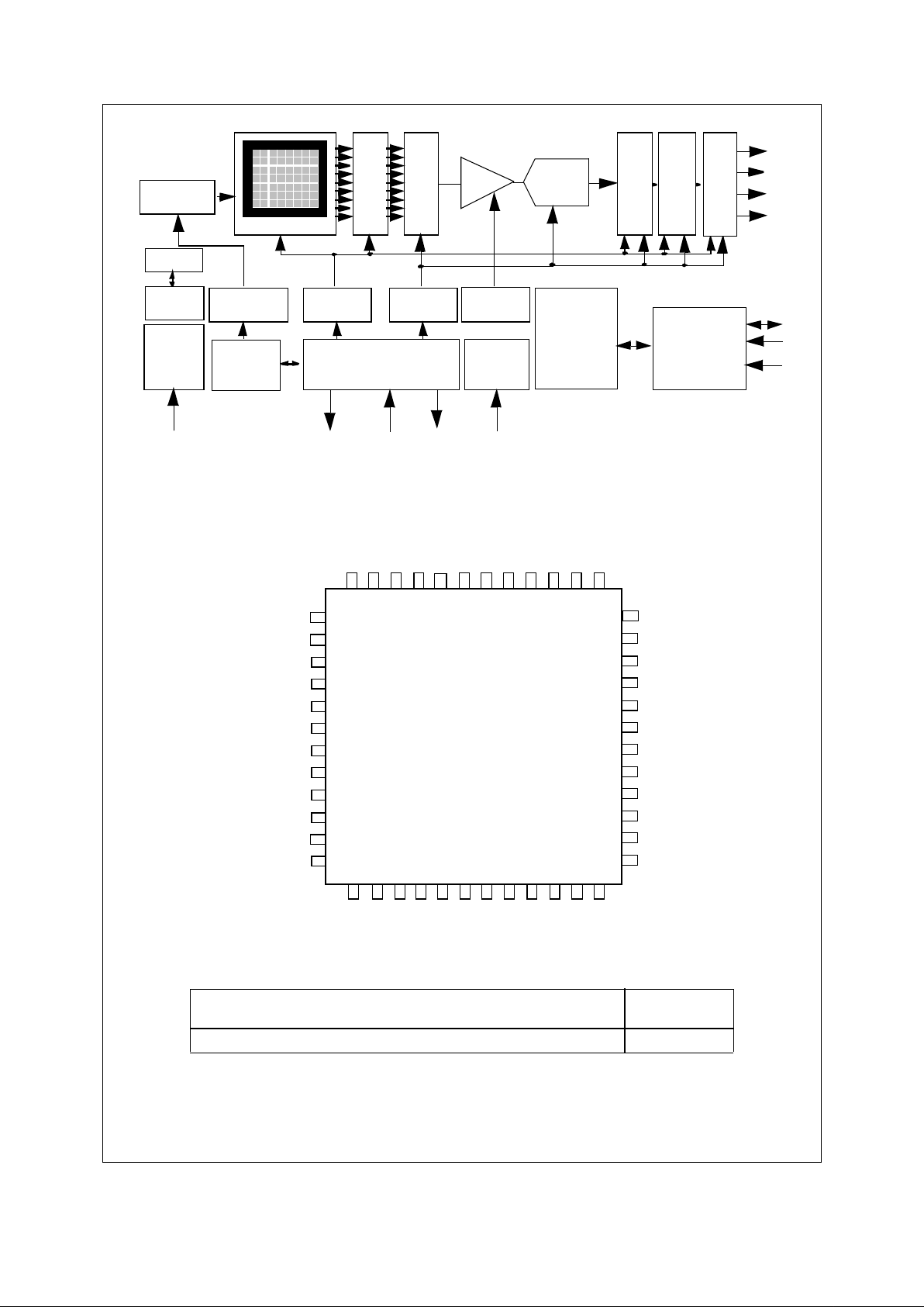
LM9617
System Block Diagram
LM9617 Monochrome CMOS Image Sensor VGA 30 FPS
Page 2
Confidential 2 www.national.com
Column CDS
APS Array
Horizontal Shif t
Register
POR
1
2 Bit A/D
AMP
Bad P ixel
Detect & Correct
Digital Video
Frame r
Black Level
Compensation
d[11:0]
pclk
hsync
vsync
Row Address
Decoder
Vertical
Horizontal
Master Timer
Timing
Timing
Row Address
Gen
Clock Gen
I2C Compatible
Register Bank
Reset
Gen
Gain
Control
Serial I/F
sda
sclk
sadr
Power
Control
pdwnsnapshot
extsync
Controller
(sequencer)
irq
mclk
Overall Chip Block Diagram
Figure 1. Chip Block Diagram
7
9
10
11
12
13
14
15
16
18
17
42
40
39
38
37
36
35
34
33
31
32
sclk
resetb
pdwn
vss_dig
vdd_dig
vsync
pclk
mclk
d1
d0
fine_i
vss_od1
vss_od3
gnd
fine_ctrl
offset
vdd_ana1
vdd_ana2
vss_ana2
sda
sadr
irq
vdd_pix
vrl
vsrvdd
extsync
vdd_od 1
6 5 4 3 2
1
48 47 46 45
NC
d4
d5
d6d8d7
d9
vdd_od2
vss_od2
19 20 21 2322 24 25 26 27 28 30
48 PIN LCC
43
d11
d10
8
snapshot
41
NC
44
vref_adc
29
d3
d2
LM9617
hsync
vss_ana1
vdd_o d3
NC
NC
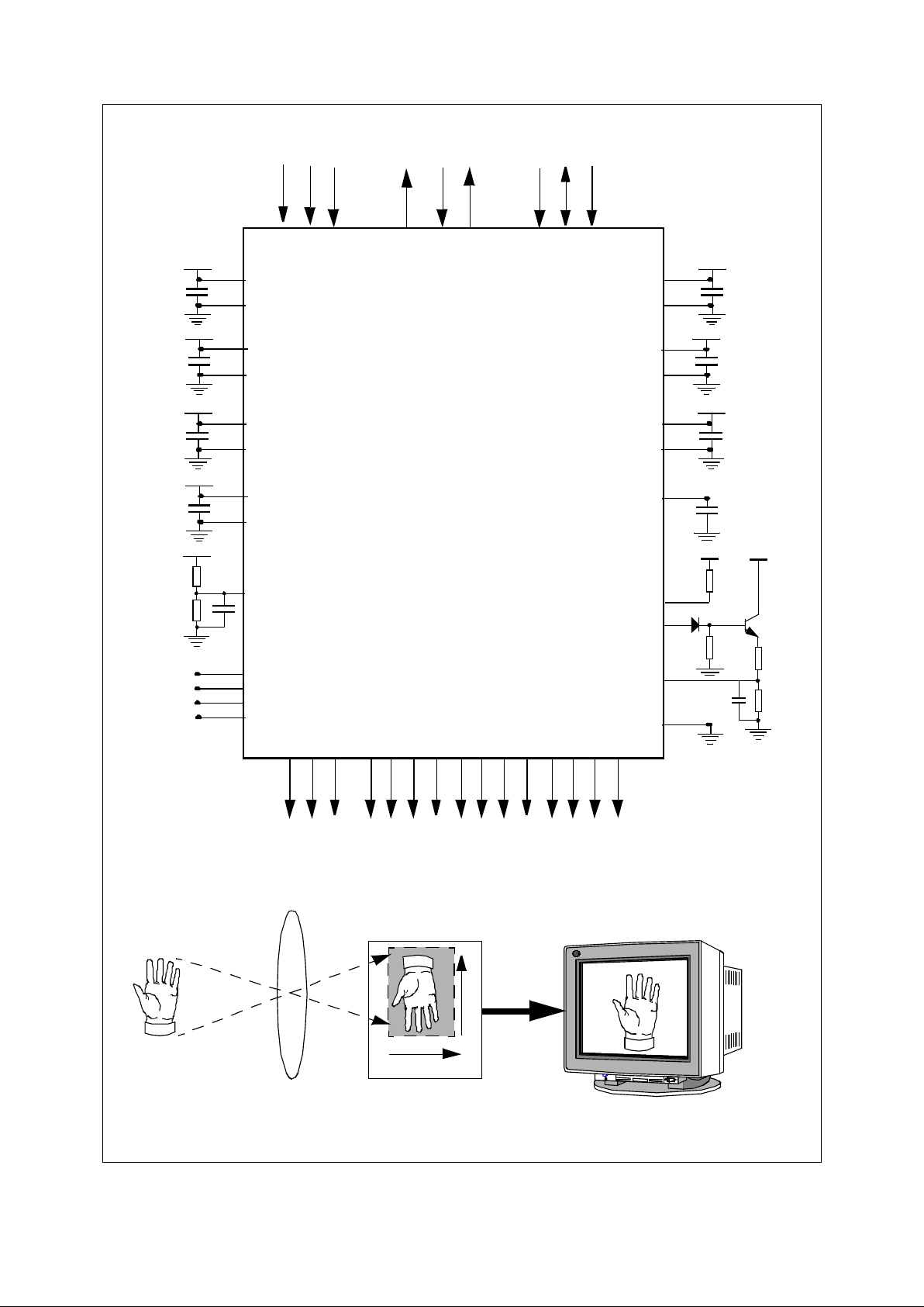
Connection Diagram
Ordering Information
Temperature
(0°C ≤ TA ≤ +50°C)
NS Package
LM9617 CCEA LCC
LM9617
Page 3
Confidential 3 www.national.com
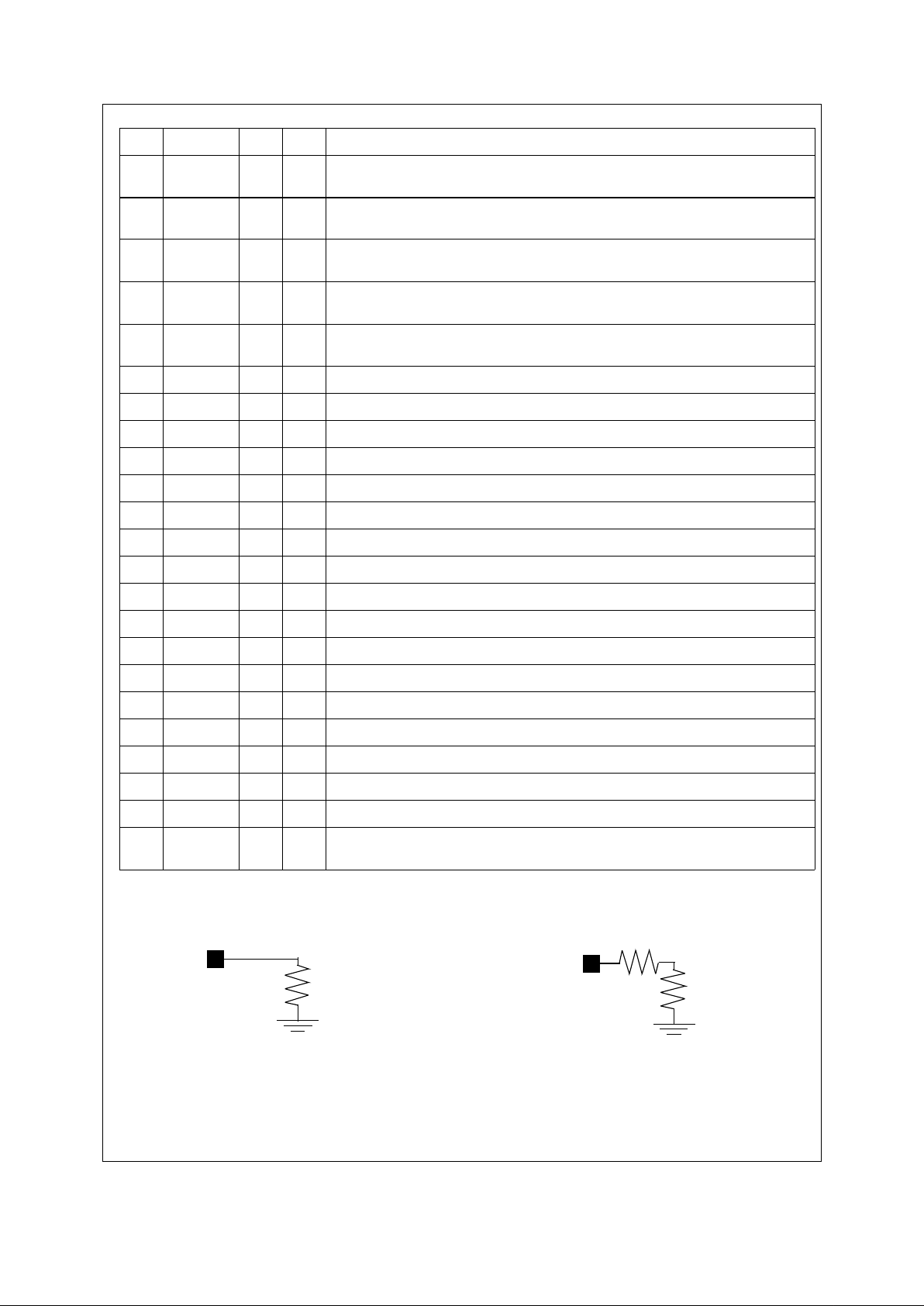
Typical Application Circuit
0.1µF
1.5k
Ω
820
Ω
3.3V analog
0.1µF
3.3V digital
12
9
37
36
35
7 6810
vss_dig
resetb
vdd_ana1
vss_ana1
vref_adc
vdd_od1
vss_od1
sadr
extsyn c
sclk
sda
d9
d8
d7d5d6
d4
d1
d0
snapshot
30 29 28 2627 25 24 23 22 21 17
d2
d3
11
vdd_dig
48 5
20
d10
d11
0.1µF
3.3V analog
31
32
vdd_od2
vss_od2
0.1µF
3.3V digital
0.1µF
3.3V digital
47
46
vdd_pix
vrl
0.1µF
3
2
1
vsrvdd
1.0µF
13 14 15
hsyn c
vsync
pclk
LM9617
pdwn
Serial Control Bus
System Control
Digital Video Bus
Camera Control
irq
4
33
34
vdd_ana2
vss_ana2
0.1µF
3.3V analog
16
mclk
vdd_od3
vss_od3
0.1µF
44
45
fine_i
41
gnd
40
3.3V analog
3.3V digital
offset
fine_ctrl
39
NC
18
NC
19
NC
42
NC
43
10kΩ
1.2kΩ
470Ω
2N3904
1N4148
4.7µF
vdd_ana
22kΩ
vdd_ana
38
1%
1%
1%
1%
Figure 2. Typical Application Diagram
Scan Read Out Direction
Figure 3. Scan directions and position of origin in imaging system
(0,0)
pin 1
CMOS Image Sensor
(0,0)
digital
out
lens
(0,0)
horizontal scan
vertical scan
LM9617
Page 4

Confidential 4 www.national.com
Pin Descriptions
Pin Name I/O Typ Description
1 vsrvdd I0 P
Analog bidirectional, it should be connect to ground via a 1.0µf capacitor. This pin is the
internal charge pump voltage source.
2 vrl I A Anti blooming pin. This pin is normally tied to ground.
3 vdd_pix I P 3.3 volt supply for the pixel array.
4 irq O D
Digital output, the interrupt request pin. This pin generates interrupts during snapshot
mode.
5 sadr I D
Digital input with pull down resistor. This pin is used to program different slave addresses
for the sensor in an I2C compatible system.
6 sda IO D
I2C compatible serial interface data bus. The output stage of this pin has an open drain
driver.
7 sclk I D I2C compatible serial interface clock.
8 snapshot I D Digital input with pull down resistor used to activate (trigger) a snapshot sequence.
9 resetb I D
Digital input with pull up resistor. When forced to a logic 0 the sensor is reset to its default
power up state. The resetb signal is internally synchronized to mclk which must be run-
ning for a reset to occur.
10 pdwn I D
Digital input with pull down resistor. When forced to a logic 1 the sensor is put into power
down mode.
11 vss_dig I P 0 volt power supply for the digital circuits.
12 vdd_dig I P 3.3 volt power supply for the digital circuits.
13 hsync IO D
Digital Bidirectional. This is a dual mode pin. When the sensor’s digital video port is con-
figured to be a master, (the default), this pin is an output and is the horizontal synchroni-
zation pulse. When the sensor’s digital video port is configured to be a slave, this pin is
an input and is the row trigger.
14 vsync IO D
Digital Bidirectional. This is a dual mode pin. When the sensor’s digital video port is con-
figured to be a master, (the default), this pin is an output and is the vertical synchroniza-
tion pulse. When the sensor’s digital video port is configured to be a slave, this pin is an
input and is the frame trigger.
15 pclk O D Digital output. The pixel clock.
16 mclk I D Digital input. The sensor’s master clock input.
17 d0 O D
Digital output. Bit 0 of the digital video output bus. This output can be put into tri-state
mode.
18 NC Pin not used, do not connect.
19 NC Pin not used, do not connect.
20 d1 O D
Digital output. Bit 1 of the digital video output bus. This output can be put into tri-state
mode.
21 d2 O D
Digital output. Bit 2 of the digital video output bus. This output can be put into tri-state
mode.
22 d3 O D
Digital output. Bit 3 of the digital video output bus. This output can be put into tri-state
mode.
23 d4 O D
Digital output. Bit 4 of the digital video output bus. This output can be put into tri-state
mode.
24 d5 O D
Digital output. Bit 5 of the digital video output bus. This output can be put into tri-state
mode.
25 d6 O D
Digital output. Bit 6 of the digital video output bus. This output can be put into tri-state
mode.
LM9617
Page 5
Confidential 5 www.national.com
Pin Descriptions (Continued)
Legend: (I=Input), (O=Output), (IO=Bi-directional), (P=Power), (D=Digital), (A=Analog).
Figure 4. Equivalent Circuits For adc_ref and offset pins
Pin Name I/O Typ Description
26 d7 O D
Digital output. Bit 7 of the digital video output bus. This output can be put into tri-state
mode.
27 d8 O D
Digital output. Bit 8 of the digital video output bus. This output can be put into tri-state
mode.
28 d9 O D
Digital output. Bit 9 of the digital video output bus. This output can be put into tri-state
mode.
29 d10 O D
Digital output. Bit 10 of the digital video output bus. This output can be put into tri-state
mode.
30 d11 O D
Digital output. Bit 11 of the digital video output bus. This output can be put into tri-state
mode.
31 vdd_od2 I P 3.3 volt supply for the digital IO buffers.
32 vss_od2 I P 0 volt supply for the digital IO buffers
33 vdd_ana2 I P 3.3 volt supply for analog circuits.
34 vss_ana2 I P 0 volt supply for analog circuits.
35 vref_adc I A A/D reference resistor ladder voltage. See figure 4 for equivalent circuit.
36 vss_ana1 I P 0 volt supply for analog circuits.
37 vdd_ana1 I P 3.3 volt supply for analog circuits.
38 offset I A Analog input used to adjust the offset of the sensor. See figure 4 for equivalent circuit.
39 fine_ctrl O A Analog output used to drive the offset pin.
40 gnd This pin must be tied to ground.
41 fine_i I A Bias current for the fine offset adjust.
42 NC Pin not used, do not connect.
43 NC Pin not used, do not connect.
44 vdd_od3 I P 3.3 volt supply for the sensor.
45 vss_od3 I P 0 volt supply for the sensor.
46 vss_od1 I P 0 volt supply for the digital IO buffers
47 vdd_od1 I P 3.3 volt supply for the digital IO buffers.
48 extsync O D
Digital output. The external event synchronization signal is used to synchronize external
events in snapshot mode.
800Ω
adc_vref
1KΩ
200Ω
offset
LM9617
Page 6
Confidential 6 www.national.com
Absolute Maximum Ratings (Notes 1 & 2)
Any Positive Supply Voltage 6.5V
Voltage On Any Input or Output Pin -0.5V to 6.5V
Input Current at any pin (Note 3) ±25mA
ESD Susceptibility (Note 5)
Human Body Model 2000V
Machine Model 200V
Package Input Current (Note 3) ±50mA
Package Power Dissipation @ TA(Note 4) 2.5W
Soldering Temperature Infrared,
10 seconds (Note 6) 220°C
Storage Temperature -40°C to 125°C
Operating Ratings (Notes 1 & 2)
Operating Temperature Range 0°C≤T≤+50°C
All VDD Supply Voltages +3.15V to +3.6V
Voltage Range on vref_adc pin +0.6V to +1.0V
Voltage Range on offset pin +0.04V to +0.4V
DC and logic level specifications
The following specifications apply for all VDD pins= +3.3V. Boldface limits apply for TA = T
MIN
to T
MAX
: all other limits TA = 25oC
(Note 7)
Power Dissipation Specifications
The following specifications apply for All VDD pins = +3.3V. Boldface limits apply for TA = T
MIN
to T
MAX
: all other limits TA = 25oC.
Symbol Parameter Conditions
Min
note 9
Typical
note 8
Max
note 9
Units
sclk, sda, sadr, Digital Input/Output Characteristics
VIH Logical “1” Input Voltage 0.7*vdd_od vdd_od+0.5 V
VIL Logical “0” Input Voltage -0.5 0.3*vdd_od V
VOL Logical “0” Output Voltage vdd_od = +3.15V, Iout=3.0mA 0.5 V
V
hys
Hysteresis (SCLK pin only) vdd_od = +3.15V
0.05*vdd_o
d
V
I
leak
Input Leakage Current Vin=vss_od -1 mA
mclk, snapshot, pdwn, resetb, hsync, vsync Digital Input Characteristics
VIH Logical “1” Input Voltage vdd_dig = +3.6V 2.0 V
VIL Logical “0” Input Voltage vdd_dig = +3.15V 0.8 V
IIH Logical “1” Input Current VIH = vdd_dig 0.1 mA
IIL Logical “0” Input Current VIL = vss_dig -1 mA
d0 - d11, pclk, hsync, vsync, extsync, irq, Digital Output Characteristics
VOH Logical “1” Output Voltage vdd_od=3.15V, Iout=-1.6mA 2.2 V
VOL Logical “0” Output Voltage vdd_od=3.15V, Iout =-1.6mA 0.5 V
IOZ TRI-STATE Output Current
VOUT = vss_od
VOUT = vdd_od
-0.1
0.1
mA
mA
IOS Output Short Circuit Current +/-17 mA
Power Supply Characteristics
IA Analog Supply Current
Power down mode, no clock.
Operational mode in dark
700
19
mA
mA
ID Digital Supply Current
Power down mode, no clock.
Operational mode in dark
300
7
mA
mA
Symbol Parameter Conditions
Min
note 9
Typical
note 8
Max
note 9
Units
P
dwn
Power Down no clock running 5 mW
PWR Average Power Dissipation
mclk = 48Mhz & sensors default settings in dark.
90 mW
LM9617
Page 7
Confidential 7 www.national.com
Video Amplifier Specifications
The following specifications apply for all VDD pins= +3.3V. Boldface limits apply for TA = T
MIN
to T
MAX
: all other limits TA = 25oC.
AC Electrical Characteristics
The following specifications apply for All VDD pins = +3.3V. Boldface limits apply for TA = T
MIN
to T
MAX
: all other limits TA = 25oC.
Note 1: Absolute Maximum Ratings indicate limits beyond which damage to the device may occur. Operating Ratings indicate con-
ditions for which the device is functional, but do not guarantee specific performance limits. For guaranteed specifications
and test conditions, see the Electrical Characteristics. The guaranteed specifications apply only for the test conditions
listed. Some performance characteristics may degrade when the device is not operated under the listed test conditions.
Note 2: All voltages are measured with respect to VSS = vss_ana = vss_od = vss_dig = 0V, unless otherwise specified.
Note 3: When the voltage at any pin exceeds the power supplies (VIN < VSS or VIN > VDD), the current at that pin should be lim-
ited to 25mA. The 50mA maximum package input current rating limits the number of pins that can safely exceed the power
supplies with an input current of 25mA.
Note 4: The absolute maximum junction temperature (TJmax) for this device is 125oC. The maximum allowable power dissipation
is dictated by TJmax, the junction-to-ambient thermal resistance (ΘJA), and the ambient temperature (TA), and can be cal-
culated using the formula PDMAX = (TJmax - TA)/ΘJA. In the 48-pin LCC, ΘJA is 38.5oC/W, so PDMAX = 2.5W at 25oC
and 1.94W at the maximum operating ambient temperature of 50oC. Note that the power dissipation of this device under
normal operation will be well under the PDMAX of the package.
Note 5: Human body model is 100pF capacitor discharged through a 1.5kΩ resistor. Machine model is 220pF discharged through
ZERO Ohms.
Note 6: See AN450, “Surface Mounting Methods and Their Effect on Product Reliability”, or the section entitled “Surface Mount”
found in any post 1986 National Semiconductor Linear Data Book, for other methods of soldering surface mount devices.
Note 7: The analog inputs are protected as shown below. Input voltage magnitude up to 500mV beyond the supply rails will not
damage this device. However, input errors will be generated If the input goes above AV+ and below AGND.
Note 8: Typical figures are at TJ = 25oC, and represent most likely parametric norms.
Note 9: Test limits are guaranteed to National's AOQL (Average Outgoing Quality Level).
Symbol Parameter Conditions
Min
note 9
Typical
note 8
Max
note 9
Units
Video Amplifier Nominal Gain 64 linear steps 0-15 dB
Symbol Parameter Conditions
Min
note 9
Typical
note 8
Max
note 9
Units
F
mclk
Input Clock Frequency 12 48 MHz
T
ch
Clock High Time @ CLK
max
10 45 ns
T
cl
Clock Low Time @ CLK
max
10 45 ns
Clock Duty Cycle @ CLK
max
45/55 55/45 min/max
Trc, TfcClock Input Rise and Fall Time 3 ns
F
hclk
Internal System Clock Frequency
1.0 14.0 MHz
T
reset
Reset pulse width 1.0 µs
FRM
rate
Frame Rate 1 30 fps
IOP
Pad
VDD
VSS
Internal Circuits
LM9617
Page 8
Confidential 8 www.national.com
CMOS Active Pixel Array Specifications
Image Sensor Specifications
The following specifications apply for All VDD pins = +3.3V, TA = 25oC, Illumination Color Temperature = 2850oK, IR cutoff filter at
700nm, mclk = 48MHz, frame rate = 30Hz, vref_adc = 0.6 volt, video gain 0dB.
Note 1: Typical figures are at TJ = 25oC, and represent most likely parametric norms.
Parameter Value Units
Number of pixels (column, row)
Total
Active
664 x 504
648 x 488
pixels
pixels
Array size (x,y Dimensions)
Total
Active
4.98 x 3.78
4.86 x 3.66
mm
mm
Pixel Pitch 7.5 µ
Fill Factor (without micro-lens) 47 %
Parameter Conditions
Min Typical
note 1
Max Units
Optical Sensitivity @ A/D output 28.7 kLSBs/(lux.s)
Optical Sensitivity @ A/D input
4.13
volt/(lux.s)
Dynamic Range 57 dB
Read Noise 5.3 LSBs
Offset Fixed Pattern Noise
RMS value of pixel FPN in dark
as a percentage of full scale.
0.35 %
Sensitivity Fixed Pattern Noise
RMS variation of pixel sensitivities as a percentage of the average sensitivity.
1 %
LM9617
Page 9
Confidential 9 www.national.com
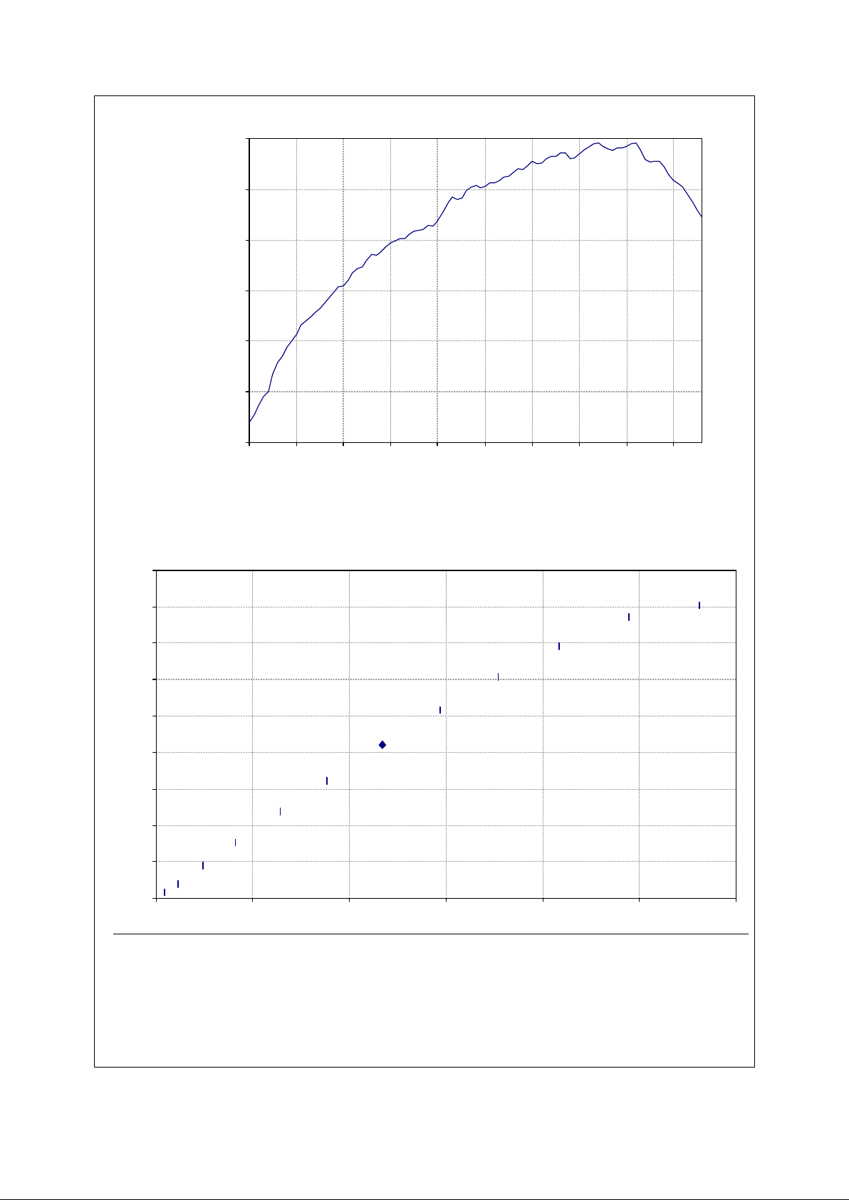
Sensor Response Curves
0.00E+00
2.00E+02
4.00E+02
6.00E+02
8.00E+02
1.00E+03
1.20E+03
370 420 470 520 570 620 670 720 770 820
wavelength [nm]
Spectral sensitivity [V/((W/m^2)*s)]
Figure 5. Spectral Response Curve
0
500
1000
1500
2000
2500
3000
3500
4000
4500
0 0.05 0.1 0.15 0.2 0.25 0.3
Exposure (lux.sec)
A/D output code
Figure 6. Linearity Response Curve
LM9617
Page 10
Confidential 10 www.national.com
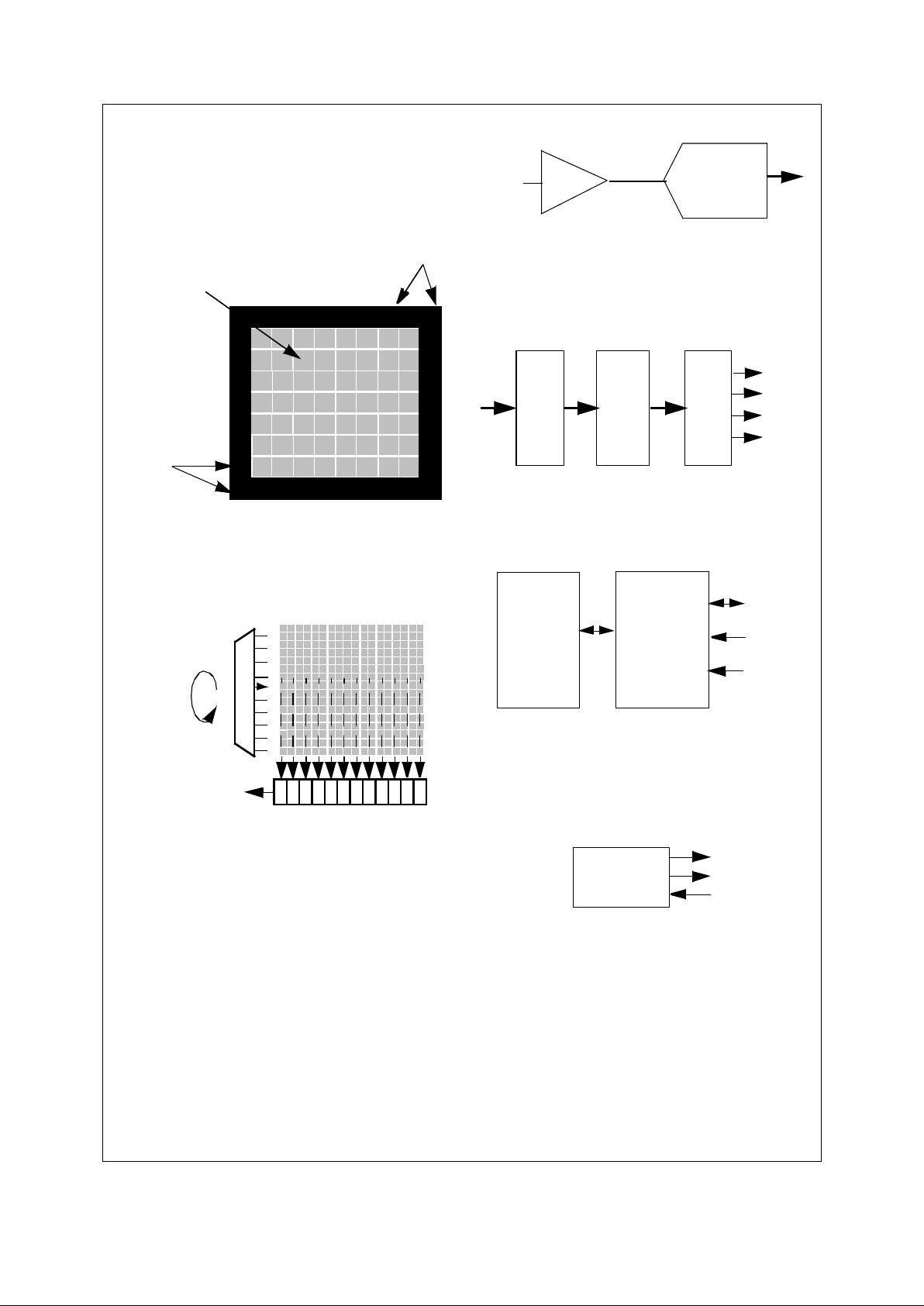
Functional Description
1.0 OVERVIEW
1.1 Light Capture and Conversion
The LM9617 contains a CMOS active pixel array consisting of
648 rows by 488 columns. This active region is surrounded by 8
columns and 8 rows of optically shielded (black) pixels as shown
in Figure.
8 columns, 8 rows
black pixels
8 columns, 8 rows
black pixels
648 columns, 488 rows
mono-chrome active pixels
Figure 7: CMOS APS region of the LM9617
At the beginning of a given integration time the on-board timing
and control circuit will reset every pixel in the array one row at a
time as shown in Figure 8. Note that all pixels in the same row
are simultaneously reset, but not all pixels in the array.
a b c d e f g h i j k l m n o p q r
0
1
2
3
4
5
6
7
8
9
10
11
12
14
13
15
CDS/Shift Register
Line Address
Analog Data Out
Figure 8: CMOS APS Row and Column addressing scheme
At the end of the integration time, the timing and control circuit
will address each row and simultaneously transfer the integrated
value of the pixel to a correlated double sampling circuit and
then to a shift register as shown in Figure 8.
Once the correlated double sampled data has been loaded into
the shift register, the timing and control circuit will shift them out
one pixel at a time starting with column “a”.
The pixel data is then fed into an analog video amplifier, where a
user programmed gain is applied .
After gain adjustment the analog value of each pixel is converted to a 12 bit digital data as shown in Figure 9.
12 Bit A/D
Video
AMP
Analog pixel values Digital pixel data
0-15dB
Figure 9: Analog Signals In, Digital Data Out.
The digital pixel data is further processed to:
• remove defects due to bad pixels,
• compensate black level, before being framed and presented
on the digital output port. (see Figure 10).
Figure 10. Digital Pixel Processing.
1.2 Program and Control Interfaces
The programming, control and status monitoring of the LM9617
is achieved through a two wire I2C compatible serial bus. In
addition, a slave address pin is provided (see Figure 11).
Figure 11. Control Interface to the LM9617.
Additional control and status pins: snapshot and external event
synchronization are provided allowing the latency of the serial
control port to be bypassed during single frame capture. An
interrupt request pin is also available allowing complex snapshot
operations to be controlled via an external micro-processor (see
Figure 12).
Figure 12. Snapshot & External Event Trigger Signals
Bad Pixel
Correction
Digital Video
Framer
Black Level
Compensation
do[11:0]
pclk
hsync
vsync
I2C Compatible
Register Bank
Serial I/F
sda
sclk
sadr
Timing
Generator
irq
snapshot
extsyn
LM9617
Page 11
Confidential 11 www.national.com
Functional Description (continued)
2.0 WINDOWING
The integrated timing and control circuit allows any size window
in any position within the active region of the array to be read out
with a 1x1 pixel resolution. The window read out is called the
“Display Window”.
A “Scan Window” must be defined first, by programing the start
and end row addresses as shown in Figure 13. Four coordinates
(start row address, start column address, end row address &
end column address) are programmed to define the size and
location of the “Display Window” to be read out (see Figure 13).
Figure 13. Windowing
Notes:
• The “Display Window” must always be defined within the
“Scan Window”.
• A “Display Window” can only be read out in the progressive
scan mode.
• By default the “Display Window” is the complete array.
2.1 Programming the scan window
Two registers (SROWS & SROWE) are provided to program the
size of the scan window. The start and end row address of the
scan window is given by:
Where:
SwStartRow
is the contents of the Scan Window start row
register (SROWS)
SwEndROW
is the contents of the Scan Window end row register (SROWE)
SwLsb
is bit 6 of the Display Window LSB register
(DWLSB)
2.2 Programming the display window
Five register (DROWS, DROWE, DCOLS, DCOLE and DWLSB)
are provided to program the display window as described in the
register section of this datasheet.
3.0 READ OUT MODES
3.1 Progressive Scan Readout Mode
In progressive scan readout mode, every pixel in every row in
the display window is consecutively read out, one pixel at a time,
starting with the left most pixel in the top most row. Hence, for
the example shown in Figure 13, the read out order will be
a0,b0,...,r0 then a1,b1,...,r1 and so on until pixel r20 is read out.
a b c d e f g h i j k l mn o p q r
1
2
3
4
5
6
7
8
9
10
11
12
13
15
14
16
17
18
19
20
Row/Vertical
0
Column/Horizontal
Figure 14: Progressive Scan Read Out Mode
3.2 Interlaced Readout Mode
In interlaced readout mode, pixels are read out in two fields, an
Odd Field followed by an Even Field.
The Odd Field, consisting of all even rows contained within the
display window, is read out first. Each pixel in the “Odd Field” is
consecutively read out, one pixel at a time, starting with the left
most pixel in the top most even row.
The Even Field, consisting of all odd rows contained within the
display window, is then read out. Each pixel in the “Even Field”
is consecutively read out, one pixel at a time, starting with the
left most pixel in the top most odd row.
a b c d e f g h i j k l mn o p q r
2
4
6
8
10
12
14
16
18
20
0
Row/Vertical
Column/Horizontal
Odd Field
1
3
5
9
7
11
13
15
17
19
Row/Vertical
Column/Horizontal
Even Field
a b c d e f g h i j k l mn o p q r
Figure 15: Interlace Read Out Mode
Hence, for the example shown in Figure , the display window is
broken up into two fields, as shown in Figure . Pixels a0,b0,...,r0
followed by a2,b2,...,r2 and so on until pixels a20,b20,...r20 in
the even field are read out first. The even field read out is followed by pixels in the odd field, a1,b1,...,r1 then a3,b3,...,r3 until
pixels a19,b19,...,r19.
display row
Active Pixel Array
Display Window
Scan Window
display row
display col
display col
start address
end address
start address
end address
scan row
start address
scan row
end address
scan row start address = (2* SwStartRow) + SwLsb
scan row end address = (2* SwEndRow) + 1 + SwLsb
LM9617
Page 12
Confidential 12 www.national.com
Functional Description (continued)
4.0 SUBSAMPLING MODES
4.1 2:1 Sub-Sampling
The timing and control circuit can be programmed to sub-sample pixels in the display window vertically, horizontally or both,
with an aspect ratio of 2:1 as illustrated in Figure16
0
1
2
3
4
5
6
7
8
9
Column/Horizontal
a b c d e f g h i j k l l n o p q r
a b c d e f g h i j k l m n o p
0
1
2
3
4
5
6
7
8
9
b) Vertical Sub-Sampling
Row/Vertical
Column/Horizontal
q
r
a b c d e f g h i j k l m n o p q r
0
1
2
3
4
5
6
7
8
Column/Horizontal
Row/Vertical
9
a) Horizontal Sub-Sampling
c) Horizontal & Vertical Sub-Sampling
Read Out
Not Read Out
Row/Vertical
Figure 16: 2:1 Horizontal and Vertical Sub-Sampling
4.2 4:2 Sub-Sampling
The timing and control circuit can be programmed to sub-sample pixels in the display window vertically, horizontally or both,
with an aspect ratio of 4:2 as illustrated in Figure17.
Column/Horizontal
a) Horizontal Sub-sampling
Read Out
Not Read Out
a b c d e f g h i j k l m n o p q r
0
1
2
3
4
5
6
7
8
9
Row/Vertical
a b c d e f g h i j k l m n o p q r
0
1
2
3
4
5
6
7
8
9
Column/Horizontal
Row/Vertical
a b c d e f g h i j k l m n o p q r
0
1
2
3
4
5
6
7
8
9
Column/Horizontal
Row/ Vertica l
c) Horizontal & Vertical Sub-sampling
b) Vertical Sub-sampling
Figure 17: 4:2 Horizontal and Vertical Sub-Sampling
LM9617
Page 13

Confidential 13 www.national.com
Functional Description (continued)
5.0 SNAPSHOT MODE
The LM9617 is capable of capturing a single frame of an image
under hardware or software control, with or without the aid of an
external shutter. Two registers, SNAPSHOTMODE0 &
SNAPSHOTMODE1, are provided to program, monitor and control all snapshot sequences.
5.1 Software Controlled Snapshots
The snapshot mode events can be software controlled by writing
to and reading from the snapshot mode registers over the I2C
compatible interface.
5.2 Hardware Controlled Snapshots
Two dedicated pins are provided on the LM9617, snapshot &
extsync, allowing the snapshot mode events to be controlled by
hardware. The snapshot pin must be enabled by writing to the
SnapEnable bit of the MCFG0 register.
5.3 Auto Snapshot Mode
In auto snapshot mode (see figure 20), upon the receipt of a
snapshot or
FTriggerNow
trigger signal, the integrated timing and
control circuit will set the FTriggerEN bit and generate an internal TRIGGER signal (see figure 19), thus resetting the array one
row at a time. At end of the reset cycle the timing and control circuit will signal the shutter to open via extsync pin or
FtSync bit.
At the end of the programmed integration time the shutter will be
signalled to close, and the pixel read-out will commence as
shown in figure 18a. At the end of the read-out sequence the
FTriggerEN will be automatically reset and the sensor will return
to video capture mode as shown in figure 20.
If an external shutter is not available then at least two frames
need to be taken so that the pixels can be integrated over one
frame as shown in Figure 18b.
To use auto snapshot mode the SsEngage bit of the
SNAPSHOTMODE1 register must be set to zero.
Note 1: This wave form shows the snapshot pin programmed to the default pulse mode.
Note 2: The irq pulse is taken low when the snapshot trigger interrupt flag (SsTrigFlag) in the snapshot mode1 (SNAPMODE1) register is read.
Note 3: The irq pulse is taken low when the snapshot trigger interrupt flag (SsRdFlag) in the snapshot mode1 (SNAPMODE1) register is read.
Figure 18. Snapshot Mode
Start Snapshot Sequence
Start of Array Reset Frames
Open Shutter
Close shutter & start read-out
Read-out complete
FTriggerEn
snapshot or FTriggerNow
extsync or FtSync
FtBusy
Array reset,
irq
programmable 1 to 4 frames
Capture
Data
read-out
image
note 1
note 2
note 3
Start Snapshot sequence
Start of Array Reset Frames
Integration Start
Start Read-out
Read-out Complete
FTriggerEn
snapshot or FTriggerNow
extsync or FtSync
FtBusy
Bold external pins
italic register bits
Array reset,
irq
programmable 1 to 4 frames
Capture Data
read-out
image
note 1
note 2
note 3
a) With External Shutter
b) Without External Shutter
LM9617
Page 14

Confidential 14 www.national.com
Functional Description (continued)
Figure 19. Snapshot Trigger Generation Logic
Figure 20. Auto Snapshot Mode State Diagram
5.4 CPU Snapshot Mode
In CPU snapshot mode, the FTriggerEN is not set automatically
and an Interrupt generator can be enabled.
Hence, upon the receipt of a snapshot or
FTriggerNow
trigger
signal, the integrated timing and control circuit will generate an
internal TRIGGER signal as shown in figure 19 and then wait in
the IRQ state for the FTriggerEN bit to be manually set as shown
in figure 21.
Once the FtriggerEn bit is set the integrated timing and control
circuit will start resetting the array one row at a time. At end of
the reset cycle the timing and control circuit will signal the shutter to open via extsync pin or
FtSync bit. At the end of the programmed integration time the shutter will be signalled to close,
and the pixel read-out will commence as shown in figure 18a. At
the end of the read-out sequence the
FTriggerEN will be automatically disabled and the sensor will return to video capture
mode as shown in figure 20.
If an external shutter is not available then at least two frames
need to be taken so that the pixels can be integrated over one
frame as shown in Figure 18b.
To use CPU snapshot mode the SsEngage bit of the
SNAPSHOTMODE1 register must be set to one.
An interrupt generator can be enabled in CPU snapshot mode
by setting the SnapIntEn bit of SNAPSHOTMODE1 register. An
interrupt will be generated on the external interrupt pin, irq,
when a snapshot sequence is triggered (TRIGGER=1) or when
the array readout is complete at the end of the snapshot
sequence as shown figure 21.
Figure 21. CPU Snapshot Mode State Diagram
When an interrupt is generated by a TRIGGER event, the
SsTrigFlag bit in the SNAPSHOTMODE1 register is set. Similarly when an interrupt is generated at the completion of a readout the SsRdFlag in the SNAPSHOTMODE1 register is set.
The polarity of the irq pin can be programmed. The interrupt can
only be cleared by reading SsTrigFlag and the SsRdFlag as
shown in figure 22.
Figure 22. Interrupt Request Generation Logic
5.5 Pulse & Level Trigger Mode
The snapshot pin can be programmed to operate in pulse trigger mode where one snapshot sequence is executed per active
pulse or in level trigger mode where by snapshot sequences are
repeated as long as the level on the snapshot pin is held active.
(see figures 20 and 21).
Pulse and level trigger modes can be set by programming the
SnapshotMod bit in the SNAPSHOTMODE0 register.
snapshot
SnapShotPol
SnapEnable
FTriggerNow
TRIGGER
VIDEO
SNAP
PREVIEW
c:TRIGGER==1
c: SnapshotMod || (SnapshotMod && TRIGGER)
a:FTriggerEn=1
a:FTriggerEn=0
VIDEO
IRQ
a:SsTrigFlag=1
SNAP
c:FTriggerEn==1
PREVIEW
a: SsRdFlag = 1
a: FtTriggerEn = 0
c:TRIGGER==1
c: SsRdFlag && (SnapshotMod || (SnapshotMod && TRIGGER))
SsTrigFlag
SsRdFlag
SnapIntEn
IrqPol
irq
LM9617
Page 15

Confidential 15 www.national.com
Functional Description (continued)
6.0 CLOCK GENERATION MODULE
The LM9617 contains a clock generation module that will create
two clocks as follows:
Hclk, the horizontal clock. This is an internal system
clock and can be programmed to be the input
clock (mclk) or mclk divided by any number
between 1 and 255.
CLK
pixel
the pixel clock. This is the external pixel clock
that appears at the digital video port. It can be
Hclk or Hclk divided by 2. This clock cannot be
programed.
7.0 FRAME RATE PROGRAMING
A frame is defined as the time it takes to reset every pixel in the
array, integrate the incident light, convert it to digital data and
present it on the digital video port. This is not a concurrent process and is characterized in a series of events each needing a
certain amount of time as shown in Figure 23.
Figure 23. Frame Readout Flow Diagram
7.1 Full Frame Integration
Full frame integration is when each pixel in the array integrates
light incident on it for the duration of a frame (see Figure 24).
The number of Hclk clock cycles required to process & shift out
one row of pixels is given by:
Where:
R
opcycle
is a fixed integer value of 780 representing the
Row Operation Cycle Time in multiples of Hclk
clock cycles. It is the time required to carry out
all fixed row operations outlined in Figure 23.
R
delay
a programmable value between 0 & 2047 repre-
senting the Row Delay Time in multiples of Hclk.
This parameter allows the Row Operation Cycle
time to be extended. (See the Row Delay High
and Row Delay Low registers).
The number of rows in a scan window is given by:
Where:
RAD
end
is the end row address of the defined scan window. (See section 2.1)
RAD
start
is the start row address of the defined scan window. (Scan section 2.1).
The number of Hclk clocks required to process a full frame is
given by:
Where:
M
factor
is a Mode Factor which must be applied. It is
dependent on the selected mode of operation as
shown in the table below:
SWN
rows
is the Number of Rows in Selected Scan Win-
dow.
F
delay
a programmable value between 0 & 4097 repre-
senting the Inter Frame Delay in multiples of
RN
Hclk
. This parameter allows the frame time to
be extended. (See the Frame Delay High and
Frame Delay Low registers).
The frame rate is given by:
7.2 Partial Frame Integration
In some cases it is desirable to reduce the time during which the
pixels in the array are allowed to integrate incident light without
changing the frame rate.
This is known as Partial Fame Integration and can be achieved
by resetting pixels in a given row ahead of the row being
selected for readout as shown in Figure 24. The number of Hclk
clocks required to process a partial frame is given by:
Where:
RN
Hclk
is the number of Hclk clock cycles required to
process & shift out one row of pixels.
I
time
is the number of rows ahead of the current row
to be reset. (See the Integration Time High and
Low registers).
The Integration time is subject to the following limits:
Start
Row address = 0
Row delay time
Transfer all pixels to CDS
Shift all pixels out of row
Row address + 1
Last row?
Reset all pixels in row
Yes
No
Row Time
RN
Hclk
= R
opcycle
+ R
delay
Progressive Scan 1
Sub-sampling or Interlace/
Interlace
0.5
Mode Limit
Progressive Scan I
time <=
SWN
rows + Fdelay
Interlace I
time <=
SWN
rows + 2*Fdelay
Sub-Sampled I
time <=
SWN
rows +
0.5*F
delay
SWN
rows
= (RAD
end
- RAD
start
) + 1
FN
Hclk
= [(M
factor *
SWN
rows
) + F
delay] *
RN
Hclk
Hclk
FN
Hclk
Frame Rate =
FP
Hclk
= RN
Hclk * Itime
LM9617
Page 16

Confidential 16 www.national.com
Functional Description (continued)
Figure 24. Partial and Full Frame Integration
7.3 Frame Rate Programming Guide
The table bellow can be used as a guide for programming the sensor. Note that it is assumed that the sensor is being driven with a
48MHz clock. All programmed values are given in decimal.
register vclkgen rdelayh rdelayl fdelayh fdelayl srows srowe dwlsb
address 05hex 15hex 16hex 17hex 18hex 0Bhex 0Chex 12hex
fps [10:8] [7:0] [11:8] [7:0] [8:1] [8:1]
30 4 0 0 0 9 0 251 50
15 4 0 0 2 40 0 251 50
7.5 4 0 0 6 12 0 251 50
3.75 4 3 12 6 12 0 251 50
25 4 0 172 0 0 0 251 50
12.5 5 0 0 1 226 0 251 50
6.25 5 0 0 5 188 0 251 50
3.125 4 0 156 14 14 0 251 50
5 4 2 255 4 23 0 251 50
4 5 0 0 10 12 0 251 50
3 5 0 0 14 14 0 251 50
2 6 0 200 13 248 0 251 50
1 6 3 241 15 126 0 251 50
Row x
Programmable Row Delay Row CDS, Reset Row x & Shift
Programmable Row Delay Row CDS, Reset Row x+∆ & Shift
Partial Frame Integration
Full Frame integration
Row n
Row 0 Row 1
Frame
Row x+∆Row n
Frame
Row 0
Full Integration Time
Row 2
Frame N
Delay Delay
Partial Integration
Time
LM9617
Page 17

Confidential 17 www.national.com
Functional Description (continued)
8.0 SIGNAL PROCESSING
8.1 Bad Pixel Detection & Correction
The LM9617 has a built-in bad pixel detection and correction
block that operates on the fly. This block can be switched off by
the user.
8.2 Black Level Compensation
In addition to the programmable gain the LM9617 has a built in
black level compensation block as illustrated in Figure 25. This
block can be switched off.
Figure 25. Digital Black Level Compensation.
The black level compensation block will subtract the average
signal level of the black pixels around the array from the digital
video output to compensate for the temperature and integration
time dependent dark signal level of the pixels. The exponential
averaging circuit shown in figure 25 only operates on the least
significant 8 bits of the video data.
9.0 POWER MANAGMENT
9.1 Power Up and Down
The LM9617 is equipped with an on-board power management
system allowing the analog and digital circuitry to be switched
off (power down) and on (power up) at any time.
The sensor can be put into power down mode by asserting a
logic one on the “pdwn” pin or by writing to the power down bit in
the main configuration register via the I2C compatible serial
interface.
To power up the sensor a logic zero can be asserted on the
“pdwn” pin or write to the power down bit in the main configura-
tion register via the I2C compatible serial interface.
It will take a few milli seconds for all the circuits to power up. The
power management register contains a bit indicating when the
sensor is ready for use. During this time the sensor cannot be
used for capturing images. A status bit in the power management register will indicate when the sensor is ready for use.
9.2 Advanced Power Features
In addition to the power up/power down features of the sensor,
sections of the analog video processing chain can be powered
down and re-routed during normal operation. This flexibility
allows power dissipation to be traded of with signal gain as
shown in the table below:
Figure 26. Power Control
10.0 ANALOG GAIN ADJUSTMENT
The integrated analog programmable gain amplifier is capable
of applying a linear gain 1X to 5.6X in 64 linear steps. This can
be programmed using the VGAIN register as shown in the table
below:
PGA Amp Power Saving
on 0mW
off 10mW
*
a
*
(1-a)
+
-
+
+
Σ
z
-1
only enabled for black pixels
input signal
com pensated output
Σ
VidGain
Dec
Code
VidGain
Hex
Code
Gain
Amp
Value
VidGain
Dec
Code
VidGain
Hex
Code
Gain
Amp
Value
0 00 1 32 20 3.34
1 01 1.07 33 21 3.41
2 02 1.15 34 22 3.48
3 03 1.22 35 23 3.56
4 04 1.29 36 24 3.63
5 05 1.37 37 25 3.7
6 06 1.44 38 26 3.77
7 07 1.51 39 27 3.85
8 08 1.58 40 28 3.92
9 09 1.66 41 29 3.99
10 0A 1.73 42 2A 4.07
11 0B 1.8 43 2B 4.14
12 0C 1.88 44 2C 4.21
13 0D 1.95 45 2D 4.29
14 0E 2.02 46 2E 4.36
15 0F 2.1 47 2F 4.43
16 10 2.17 48 30 4.5
17 11 2.24 49 31 4.58
18 12 2.31 50 32 4.65
19 13 2.39 51 33 4.72
20 14 2.46 52 34 4.8
21 15 2.53 53 35 4.87
22 16 2.61 54 36 4.94
23 17 2.68 55 37 5.02
24 18 2.75 56 38 5.09
25 19 2.83 57 39 5.16
26 1A 2.9 58 3A 5.23
27 1B 2.97 59 3B 5.31
28 1C 3.04 60 3C 5.38
29 1D 3.12 61 3D 5.45
30 1E 3.19 62 3E 5.53
31 1F 3.26 63 3F 5.6
LM9617
Page 18

Confidential 18 www.national.com
Functional Description (continued)
11.0 OFFSET ADJUSTMENT
For maximum image quality over a wide range of light conditions
it is necessary to set an appropriate offset voltage before using
the sensor to capture images. This offset voltage must be
applied to the offset pin (38) of the sensor, and is used to adjust
the analogue video signal being fed to the internal A/D.
The level of the offset voltage determines the black level of the
image and has a direct impact on the image quality. Too high an
offset results in a white washed or hazy looking image, while too
low of an offset results in a dark image with low contrast even
though the light conditions are good.
A fine offset adjustment should be applied to each part by programming the offset voltage via the I2C compatible serial inter-
face. To program an offset voltage the following procedure
should be followed:
The sensor’s offset, fine_i & fine_ctrl pins should be connected
as shown in figure 2.
The following procedure should be followed to calibrate the offset
• Disable the black level compensation block by writing a logic
1 to bit 4 of the Main Configuration Register 0 (MCFG0:
address 02Hex).
• The offset can be adjusted by writing to the Offset Compen-
sation Registers (OCR: addresses 1F, 22 & 25 hex). Writing
00hex will give the largest voltage, while writing FF hex will
give the smallest value.
• Run the following binary search algorithm
• For n=7 to 0 step -1
• {
Set bit n in the OCR registers (addresses 1F, 22 & 25
Hex) to a logic one by writing over the I2C compatible
interface.
Read a full frame and calculate the average black level
(BL
average
) of the first and last 5 black pixels in the every
row of the array
If (BL
average
< 100) then
Reset bit n in the OCR registers (addresses 1F, 22 &
25 Hex) to 0
else
Keep bit n set to one.
}
• Enable the black level compensation block (if desired) by writing a logic 0 to bit 4 of the Main Configuration Register 0
(MCFG0: address 02Hex).
12.0 OFFSET & GAIN
The fine offset adjustment and calibration method described in
section 11.0 will ensure that the sensor’s black level is optimized
for a fixed analog gain setting. However, when the analog gain is
changed substantially, the black level of the sensor will shift
resulting in a white washed image.
To stop this effect from occurring, the black level needs to be recalibrated. This can be done as part of the contrast adjustment
which is carried out by most digital image processors. If this is
not possible then the following method can be used.
The relationship between the gain and the offset can be
described with the following equation.
where:
Offset(G) is the offset that needs to be programmed in
the OCR1, OCR2 & OCR3 registers to ensure
the correct black level setting for an analog
gain setting of G.
Offset(0) is the offset that needs to be programmed in
the OCR1, OCR2 & OCR3 registers to ensure
the correct black level setting for unity analog
gain, (G=0).
C is a constant and will vary from sensor to sen-
sor
G is the value programmed in the VGAIN regis-
ter of the sensor which determines the sen-
sor’s analog gain.
The following procedure should be used to calculate the value of
C:
Use the calibration procedure described in section 11.0 to determine the offset at unity gain, offset(0). Note the VGAIN register
should be set to 0.
Set the sensor’s analog gain register (VGAIN) to its max setting,
31, and repeat the calibration procedure described in section
11.0. This will allow the offset at full gain, 31, that needs to be
programmed in the OCR1, OCR2 & OCR3 registers to ensure
the correct black level setting to be determined.
The value of C for a particular sensor can be calculated using
the following formula:
Once the value of C has been calculated, offset values for different gain settings can be calculated using equation 1. It is recommended that a two decimal point accuracy for C is maintained.
Offset(G) = Offset(0) + C * G
0.4
Offset(31) - Offset(0)
3.95
C =
LM9617
Page 19

Confidential 19 www.national.com
Functional Description (continued)
13.0 SERIAL BUS
The serial bus interface consists of the sda (serial data), sclk
(serial clock) and sadr (device address select) pins. The
LM9617 can operate only as a slave.
The sclk pin is an input, it only and controls the serial interface,
all other clock functions within LM9617 use the master clock pin,
mclk.
13.1 Start/Stop Conditions
The serial bus will recognize a logic 1 to logic 0 transition on the
sda pin while the sclk pin is at logic 1 as the start condition. A
logic 0 to logic 1 transition on the sda pin while the sclk pin is at
logic 1 is interrupted as the stop condition as shown in Figure
27.
Figure 27. Start/Stop Conditions
13.2 Device Address
The serial bus Device Address of the LM9617 is set to 1010101
when sadr is tied low and 0110011 when sadr is tied high. The
value for sadr is set at power up.
13.3 Acknowledgment
The LM9617 will hold the value of the sda pin to a logic 0 during
the logic 1 state of the Acknowledge clock pulse on sclk as
shown in Figure 28.
Figure 28. Acknowledge
13.4 Data Valid
The master must ensure that data is stable during the logic 1
state of the sclk pin. All transitions on the sda pin can only occur
when the logic level on the sclk pin is “0” as shown in Figure 29.
Figure 29. Data Validity
13.5 Byte Format
Every byte consists of 8 bits. Each byte transferred on the bus
must be followed by an Acknowledge. The most significant bit of
the byte is should always be transmitted first. See Figure 30.
13.6 Write Operation
A write operation is initiated by the master with a Start Condition
followed by the sensor’s Device Address and Write bit. When
the master receives an Acknowledge from the sensor it can
transmit 8 bit internal register address. The sensor will respond
with a second Acknowledge signaling the master to transmit 8
write data bits. A third Acknowledge is issued by the sensor
when the data has been successfully received.
The write operation is completed when the master asserts a
Stop Condition or a second Start Condition. See Figure 31.
13.7 Read Operation
A read operation is initiated by the master with a Start Condition
followed by the sensor’s Device Address and Write bit. When
the master receives an Acknowledge from the sensor it can
transmit the internal Register Address byte. The sensor will
respond with a second Acknowledge. The master must then
issue a new Start Condition followed by the sensor’s Device
Address and read bit. The sensor will respond with an Acknowledged followed by the Read Data byte.
The read operation is completed when the master asserts a Not
Acknowledge followed by Stop Condition or a second Start Condition. See Figure 32.
sda
sclk
S P
start condition stop condition
1 2
7 8
9
sda
from master
sda
from sensor
sclk
MSB
ACK
ACK
START
S
Clock pulse
for ACK
sda
sclk
data line
stable;
data valid
change
of data
allowed
data line
stable;
data valid
Figure 30. Serial Bus Byte Format
Figure 31. Serial Bus Write Operation
Figure 32. Serial Bus Read Operation
sclk
sda
1 2
7
8
9 1
8
2
MSB
ACK
S
P
ack signal
from receiver
byte complete
clock line
held low
9
ack signal
from receiver
ACK
Address
WS A
Register
A
Data
A P
Device
Address Byte
bold sensor action
Device
S A
Register Data Device
A S AR P
_
A
ByteAddressAddress
W
Address
bold sensor action
LM9617
Page 20

Confidential 20 www.national.com
Functional Description (continued)
14.0 DIGITAL VIDEO PORT
The captured image is placed onto a flexible 12-bit digital port as
shown in Figure 10. The digital video port consists of a programmable 12-bit digital Data Out Bus (d[11:0]) and three program-
mable synchronisation signals (hsync, vsync, pclk).
By default the synchronisation signals are configured to operate
in “master” mode. They can be programed to operate in “slave”
mode.
The following sections are a detailed description of the timing
and programming modes of digital video port.
Pixel data is output on a 12-bit digital video bus. This bus can be
tri-stated by asserting the TriState bit in the VIDEOMODE1 register.
14.1 Digital Video Data Out Bus (d[11:0])
A programmable matrix switch is provided to map the output of
the internal pixel framer to the pins of the digital video bus as
illustrated in Figure 33.
Figure 33. Digital Video Bus Switching Modes
This feature allows a programmable digital gain to be implemented when connecting the sensor to 8 or 10 bit digital video
processing systems as illustrated in Figure 34. The unused bits
on the digital video bus can be optionally tri-stated.
Figure 34. Example of connection to 10/8 bit systems
Synchronisation Signals in Master Mode
By default the sensor’s digital video port’s synchronisation signals are configured to operate in master mode. In master mode
the integrated timing and control block controls the flow of data
onto the 12-bit digital port, three synchronisation outputs are
provided:
pclk is the pixel clock output pin.
hsync is the horizontal synchronisation output signal.
vsync is the vertical synchronisation output signal.
14.2 Pixel Clock Output Pin (pclk) (Master Mode)
The pixel clock output pin, pclk, is provided to act as a synchronisation reference for the pixel data appearing at the digital
video out bus pins d[11:0]. This pin can be programmed to operate in two modes:
• In free running mode the pixel clock output pin, pclk, is always
running with a fixed period. Pixel data appearing on the digital
video bus d[11:0] are synchronized to a specified active edge
of the clock as shown in Figure 35.
Figure 35. pclk in Free Running Mode
• In data ready mode, the pixel clock output pin (pclk) will pro-
duce a pulse with a specified level every time valid pixel data
appears on the digital video bus d[11:0] as shown in Figure
36.
d11
9
Internal Pixel Framer Output Register
d10 8d9 7d86d7 5d6 4d5 3d4 2d3 1d2
010
d1 d0
11
a) MSB Bit 11, Switch Mode (default)
b) MSB Bit 10, Switch Mode
d) MSB bit 8, Switch Mode
Internal Pixel Framer Output Register
d11 d10 d9 d8 d7 d6 d5 d4 d3 d2 d1 d0
9 8 7 6 5 4 3 2 1 0
1011
c) MSB bit 9, Switch Mode
d0
Internal Pixel Framer Output Register
d11 d10 d9 d8 d7 d6 d5 d4 d3 d2 d1
9 8 7 6 5 4 3 2 1 0
1011
Internal Pixel Framer Output Register
d11 d10 d9 d8 d7 d6 d5 d4 d3 d2 d1
9 8 7 6 5 4 3 2 1 01011
d0
10 bit
Digital
Image
Processor
d9d11
d8d10
d7d9
d6d8
d5d7
d4d6
d3d5
d2d4
d1d3
d0d2
d1
d0
LM9617
8 bit
Digital
Image
Processor
d7d11
d6d10
d5d9
d4d8
d3d7
d2d6
d1d5
d0d4
d3
d2
d1
d0
LM9617
a) LM9617 Connected to a 10 bit Digital Image Processors
b) LM9617 Connected to a 8 bit Digital Image Processors
pclk
d[11:0]
pclk
d[11:0]
a) pclk active edge negative
b) pclk active edge positive (default)
invalid pixel data
LM9617
Page 21

Confidential 21 www.national.com
Functional Description (continued)
,
Figure 36. pclk in Data Ready Mode
By default the pixel clock is a free running active low (pixel data
changes on the positive edge of the clock) with a period equal to
the internal hclk. The active edge of the clock can be pro-
grammed such that pixel data changes on the positive or negative edge of the clock.
14.3 Horizontal Synchronisation Output Pin (hsync)
The horizontal synchronisation output pin, hsync, is used as an
indicator for row data. The hsync output pin can be programmed
to operate in two modes as follows:
• Level mode should be used when the pixel clock, pclk, is programmed to operate in free running mode. In level mode the
hsync output pin will go to the specified level (high or low) at
the start of each row and remain at that level until the last
pixel of that row is read out on d[11:0] as shown in Figure 37.
The hsync level is always synchronized to the active edge of
pclk.
Figure 37. hsync in Level Mode
• Pulse mode should be used when the pixel clock, pclk, is programmed to operate in data ready mode. In pulse mode the
hsync output pin will produce a pulse at the end of each row.
The width of the pulse will be a minimum of four pclk cycles
and its polarity can be programmed as shown in Figure 38.
The hsync level is always synchronized to the active edge of
pclk
Figure 38. hsync in Pulse Mode
By default the first pixel data at the beginning of each row is
placed on the digital video bus as soon as hsync is activated. It
is possible to program up to 15 dummy pixels to be readout at
the beginning of each row before the real pixel data is readout.
This feature is supported for both level and pulse mode.
14.4 Vertical/Horizontal Synchronisation Pin (vsync)
The vertical synchronisation output pin, vsync, is used as an
indicator for pixel data within a frame. The vsync output pin can
be programmed to operate in two modes as follows:
• Level mode should be used when the pixel clock, pclk, is programmed to operate in free running mode. In level mode the
vsync output pin will go to the specified level (high or low) at
the start of each frame and remain at that level until the last
pixel of that row in the frame is placed on d[11:0] as shown in
Figure 39. The hsync level is always synchronized to the
active edge of pclk.
Figure 39. vsync in Level Mode
• Pulse mode should be used when the pixel clock, pclk, is pro-
grammed to operate in data ready mode. In pulse mode the
vsync output pin will produce a pulse at the end of each
frame. The width of the pulse will be a minimum of four hclk
cycles and its polarity can be programmed as shown in Figure
40. The vsync level is always synchronized to the active edge
of pclk.
Figure 40. vsync in pulse mode
14.5 Odd/Even Mode
In odd/even mode the vsync signal is used to indicate when
pixel data from an odd and even field is being placed on the digital video bus d[11:0]. The polarity of vsync can still be programmed in this mode as shown in Figure 41
Figure 41. vsync in odd/even Mode
pclk
d[11:0]
pclk
d[11:0]
a) pclk active edge negative
b) pclk active edge positive
invalid pixel data
pclk
d[11:0]
invalid pixel data
b) hsync programmed to be active low
hsync
Row n
Row n+1
pclk
d[11:0]
a) hsync programmed to be active high (default)
hsync
Row n
Row n+1
pclk
d[11:0]
hsync
Row n
Row n+1
a) hsync programmed to be active high
pclk
d[11:0]
hsync
Row n Row n+1
b) hsync programmed to be active low
invalid pixel data
pclk
d[11:0]
invalid pixel data
b) vsync programmed to be active low
vsync
Frame n
Frame n+1
pclk
d[11:0]
a) vsync programmed to be active high
vsync
Frame n
Frame n+1
pclk
d[11:0]
vsync
Frame n
Frame n+1
a) vsync programmed to be active high
pclk
d[11:0]
vsync
Frame n
Frame n+1
b) vsync programmed to be active low (default)
invalid pixel data
pclk
d[11:0]
invalid pixel data
b) vsync programmed to be active low
vsync
Odd Field
Even Field
pclk
d[11:0]
a) vsync programmed to be active high (default)
vsync
Odd Field
Even Field
LM9617
Page 22

Confidential 22 www.national.com
Functional Description (continued)
Figure 42. Example of Digital Video Port Timing in Progressive Scan Mode
Figure 43. Example of Digital Video Port Timing in Interlaced Mode
Figure 44. Example of Digital Video Port Timing in 2:1 Sub-sampling Mode
Figure 45. Example of Digital Video Port Timing in 4:2 Sub-sampling Mode
c0 c1 c2 c3 c4 c5 c6 c7 c8 c9
c0 c1 c2 c3 c4 c5 c6 c7 c8 c9
pclk
vsync
hsync
d[11:0]
c0 c1 c2 c3 c4 c5 c6 c7 c8 c9 c0 c1 c2 c3 c4 c5 c6 c7 c8 c9
frame 1
row1
row 2
row 1
row 2
frame 2
Programmable hsync to 1st valid pixel delay
Programmable inter-frame delay
Programmable row delay
c0 c1 c2 c3 c4 c5 c6 c7 c8 c9 c0 c1 c2 c3 c4 c5 c6 c7 c8 c9
pclk
vsync
hsync
d[11:0]
c0 c1 c2 c3 c4 c5 c6 c7 c8 c9 c0 c1 c2 c3 c4 c5 c6 c7 c8 c9
Odd Field
row1 row 3 row 2 row 4
Even Field
Programmable hsync to 1st valid pixel delay
Programmable inter-frame delay
Programmable row delay
c0 c2 c 4 c6 c8 c0 c2 c4 c6 c8
pclk
vsync
hysync
d[11:0]
c0 c2 c4 c6 c8 c0 c2 c4 c6 c8
row 3
frame 1 frame 2
row 1row 3row 1
Programmable hsync to 1st valid pixel delay
Programmable inter-frame delay
Programmable inter-row delay
c0 c2 c4 c6 c8 c0 c2 c4 c5 c8
pclk
vsync
hsync
d[11:0]
c0 c2 c4 c6 c8 c0 c2 c4 c6 c8
row 2
frame 1 frame 2
row 1row 2row 1
Programmable hsync to 1st valid pixel delay
Programmable inter-frame delay
Programmable inter-row delay
LM9617
Page 23

Confidential 23 www.national.com
Functional Description (continued)
14.6 Synchronisation Signals in Slave Mode
The sensor’s digital video port’s synchronisation signals can be
programmed to operate in slave mode. In slave mode the integrated timing and control block will only start frame and row processing upon the receipt of triggers from an external source.
Only two synchronization signals are used in slave mode as follows:
hsync is the row trigger input signal.
vsync is the frame trigger input signal.
Figure 46 shows the LM9617’s digital video port in slave mode
connected to a digital video processor master DVP.
Figure 46. LM9617 in slave mode
14.7 Row Trigger Input Pin (hsync)
The row trigger input pin, hsync, is used to trigger the processing of a given row. It must be activated for at least two “mclk”
cycle. The first pixel data will appear at d[11:0] “X
mclk
“periods
after the assertion of the row trigger, were X
mclk
is given by:
Where:
DW
StAd
is the value of the display window column start
address.
The polarity of the active level of the row trigger is programmable. By default it is active high.
14.8 Frame Trigger Input Pin (vsync)
The frame trigger input pin, vsync, is used to reset the row
address counter and prepare the array for row processing. It
must be activated for at least one “mclk” cycle and no more than
96 mclk cycles after the activation of hsync as illustrated in Figure 48.
The polarity of the active level of the row trigger is programmable. By default it is active high.
RowTrig
FrameTrig
MasterClock
din[11:0]d[11:0]
hsync
vsync
pclk
mclk
DVP
LM9617
X
mclk
= 124 + DW
StAd
Figure 47. hsync slave mode timing diagram for centred display window of 642 pixels
Figure 48. vsync slave mode timing diagram for scan window of 504 rows.
779778777776 0 1 32 134 135 136 136 137 779778777 0 1776775774... ...
hsync
pixel 11
pixel 12
pixel 652
d[11:0]
mclk
mclk
count
642 valid pixels
780 clock cycles per line
779778777776 0 1 32 779778777 0 1776775774...
hsync
mclk
mclk
count
780 clock cycles per line
internal row
counter
line502
line 502
No more than
96 clock cycles
vsync
...
779778777 0 1776775774
line503 line 0
LM9617
Page 24

Confidential 24 www.national.com
MEMORY MAP
ADDR Register Reset Value Description
00h Reserved for future use.
01h REV 02h Revision Register
02h MCFG0 00h Main Configuration Register 0
03h MCFG1 00h Main Configuration Register 1
04h PCR 00h Power Control Register.
05h VCLKGEN 04h Video Clock Generator
06h VMODE0 00h Video Mode 0 Register
07h VMODE1 00h Video Mode 1 Register
08h VMODE2 00h Video Mode 2 Register
09h SNAPMODE0 00h Snapshot Mode 0 Register
0Ah SNAPMODE1 00h Snapshot Mode 1 Register
0Bh SROWS 00h Scan Window Row Start Register
0Ch SROWE FBh Scan Window Row End Register
0Dh Reserved for future use.
0Eh DROWS 00h Display Window Row Start Register
0Fh DROWE FBh Display Window Row End Register
10h DCOLS 00h Display Window Column Start Register
11h DCOLE A5h Display Window Column End Register
12h DWLSB 32h Display Window LSB Register.
13h ITIMEH 00h Integration Time High Register
14h ITIMEL 00h Integration Time Low Register
15h RDELAYH 00h Row Delay High Register
16h RDELAYL 00h Row Delay Low Register
17h FDELAYH 00h Frame Delay High Register
18h FDELAYL 00h Frame Delay Low Register
19h VGAIN 00h Video Gain Register
1Fh OCR1 00h Offset Compensation Register 1
22h OCR1 00h Offset Compensation Register 1
25h OCR2 00h Offset Compensation Register 2
26h BLCOEFF 00h Black Level Compensation Coefficient Register
27h BPTH0H 00h Bad pixel Threshold 0 High Register
28h BPTH0L 00h Bad pixel Threshold 0 Low Register
29h BPTH1H 00h Bad pixel Threshold 1 High Register
2Ah BPTH1L 00h Bad pixel Threshold 1 Low Register
LM9617
Page 25

Confidential 25 www.national.com
Register Set
The following section describes all available registers in the
LM9617 register bank and their function.
Register Name Device Rev Register
Mnemonic REV
Address 01 Hex
Type Read Only.
Register Name Main Configuration 0
Address 02 Hex
Mnemonic MCFG0
Type: Read/Write
Reset Value 00 Hex
Register Name Main Configuration 1
Address 03 Hex
Mnemonic MCFG1
Type Read/Write
Reset Value 00 Hex
Register Name Power Control Register 1
Address 04 Hex
Mnemonic PCR
Type Read/Write
Reset Value 00 Hex
Bit Bit Symbol Description
7:0 SiRev The silicon revision register.
Bit Bit Symbol Description
7 PwrUpBusy (Read Only Bit)
Indicates that power on initialization is in progress. The sensor is
ready for use when this bit is at
logic 0.
6 PwrDown Assert to power down the sensor.
Writing a logic 1 to this register bit
has the same effect as taking the
pdwn pin high. Clear (the default)
this bit to power up the sensor.
5 BPCorrection Assert to enable the bad pixel
detection and correction circuit.
Clear (the default) to switch it off.
4 BlkLComp Assert to disable the black level
compensation circuit. Clear (the
default) to switch it on.
3 SnapEnable Assert to enable the external
snapshot pin. Clear (the default)
to disable the external snapshot
pin.
2:0 Reserved
Bit Bit Symbol Description
7 ColorMode Assert when using a mono-
chrome sensor. When this bit is
at a logic 1, Sub-Sampling is set
to 2:1 and every other row is
read out during interlace mode.
Clear (the default) when using a
color sensor. When this bit is at
logic 0, sub-sampling is set to
4:2 and every other row pair is
read out during interlace mode.
6 ScanMode Assert to set the sensor to inter-
lace readout mode. Clear (the
default) to set the sensor to progressive scan read out mode.
5 HSubSamEn Assert to enable horizontal sub-
sampling. Clear (the default) to
disable horizontal sub-sampling.
4 VSubSamEn Assert to enable vertical sub-
sampling. Clear (the default) to
disable vertical sub-sampling.
3 Reserved
2 SlaveMode Use to configure the digital
video port’s synchronisation sig-
nal to operate in slave mode. By
default the digital video’s port’s
synchronization signals are con-
figured to operate in master
mode.
1:0 Reserved
Bit Bit Symbol Description
7 ByPassGain Assert to route the analog video
signal from the output of the CDS
to the input of the 12 bit A/D. Clear
(the default) to route the signal to
the video gain amplifier.
6:4 Reserved
3 PwdnPGA Assert to power down the pro-
grammable video gain amplifier.
Clear (the default) to power up the
video gain amplifiers.
2:1 Reserved
0 PwDnADC Assert to power down the 12 bit
analog to digital convertor. Clear
(the default) to power up the 12 bit
analog to digital convertor.
LM9617
Page 26

Confidential 26 www.national.com
Register Set (continued)
Register Name Hclk Generator Register
Address 05 Hex
Mnemonic VCLKGEN
Type Read/Write
Reset Value 04 Hex.
Register Name Digital Video Mode 0
Address 06 Hex
Mnemonic VMODE0
Type Read/Write
Reset Value 00 Hex
Register Name Digital Video Mode 1
Address 07 Hex
Mnemonic VMODE1
Type Read/Write
Reset Value 00 Hext
Register Name Digital Video Mode 2
Address 08 Hex
Mnemonic VMODE2
Type Read/Write
Reset Value 00 Hex
Bit Bit Symbol Description
7:0 HclkGen Use to divide the frequency of
the sensors master clock input,
mclk to generate the internal
sensor clock, Hclk.
Program 00 Hex (the default) for
Hclk to equal mclk or divide
mclk by any number between 1
and FF Hex.
Bit Bit Symbol Description
7:6 PixDataSel Use to program the number of
active bits on the digital video bus
d[11:0], starting from the MSB
(d[11]). Inactive bits are tri-stated.:
5:4 PixDataMsb Use to program the routing of the
MSB output of the internal video
A/D to a bit on the digital video
bus.
3:0 Reserved
00 12 bit mode, bits
d[11:0] of the digital
video bus are active.
This is the default.
01 10 bit mode, bits
d[11:2] of the digital
video bus are active.
10 8 bit mode, bits
d[11:4] of the digital
video bus are active.
11 Reserved.
00 A/D [11:0] -> d[11:0].
01 A/D [10:0] -> d[11:1]
10 A/D [9:0] -> d[11:2]
11 A/D [8:0] -> d[11:3]
Bit Bit Symbol Description
7 PixClkMode Assert to set the pclk to “data
ready mode”. Clear, the default, to
set pclk to “free running mode”.
6 VsyncMode Assert to set the vsync pin to
“pulse mode”. Clear (the default)
to set the vsync signal to “level
mode”.
5 HsyncMode Assert to force the hsync signal to
pulse for a minimum of four pixel
clocks at the end of each row.
Clear (the default) to force the
hsync signal to a level indicating
valid data within a row.
4 PixClkPol Assert to set the active edge of
the pixel clock to negative. Clear
(the default) to set the active edge
of the clock to positive.
3 VsynPol Assert to force the vsync signal to
generate a logic 0 during a frame
readout (Level Mode), or a nega-
tive pulse at the end of a frame
readout (Pulse Mode). Clear (the
default) to force the vsync signal
to generate a logic 1 during a
frame readout (Level Mode), or a
negative pulse at the end of a
frame readout (Pulse Mode).
2 HsynPol Assert to force the hsync signal to
generate a logic 0 during a row
readout (Level Mode), or a nega-
tive pulse at the end of a row
readout (Pulse Mode). Clear (the
default) to force the hsync signal
to generate a logic 1 during a row
readout (Level Mode), or a nega-
tive pulse at the end of a readout
(Pulse Mode).
1 OddEvenEn Assert to force the vsync pin to act
as an odd/even field indicator.
Clear (the default) to force the
vsync pin to act as a vertical syn-
chronization signal.
0 TriState Assert to tri-state all output signals
(data and control) on the digital
video port. Clear (default) to
enable all signals (data and con-
trol) on the digital video port.
Bit Bit Symbol Description
7:4 HsyncAdjust Use to program the leading edge
of hsync to the first valid pixel at
the beginning of each row. This
can be 0-hex to F-hex corre-
sponding to 0 - 15 pixel clocks.
Default 0.
3:0 Reserved
LM9617
Page 27

Confidential 27 www.national.com
Register Set (continued)
Register Name Snapshot Mode Configuration Register 0
Address 09 Hex
Mnemonic SNAPMODE0
Type Read/Write
Reset Value 00 Hex
Register Name Snapshot Mode Configuration Register 1
Address 0A Hex
Mnemonic SNAPMODE1
Type Read/Write
Reset Value 00 Hex.
Bit Bit Symbol Description
7.6 SsFrames Program to set the number of
frames required before readout
during a snapshot with no external
shutter, (see Figure 18). By
default these two bits are set to 00
resulting in one frame before
readout:
5 ShutterEn Assert to indicate that an external
shutter will be used during snapshot mode. Clear (the default) to
indicate that snapshot mode will
be carried out without the aid of an
external shutter.
4 ExtSynPol Assert to set the active level of the
extsync signal to 0. Clear (the
default) to set the active level of
the extsync signal to 1.
3 Reserved
2 SnapshotMod Assert to set the snapshot pin to
level mode. In level mode the sensor will continually run snapshot
sequences as long as the snap-
shot pin is held to the active level.
Clear (the default) to set the snap-
shot signal to pulse mode. In
pulse mode the sensor will only
carry out one snapshot sequence
per pulse applied to the snapshot
pin.
1 SnapShotPol Assert to set the snapshot pin to
be active on the positive edge.
Clear (the default) to set the snapshot pin to be active on the negative edge.
0 IrqPol Assert to set the active level of the
irq signal to 0, Clear (the default)
to set the active level of the irq
signal to 1.
0 one frame
01 two frames
10 three frames
11 four frames
Bit Bit Symbol Description
7 SnapIntEn Assert to enable the snapshot
interrupt generator. Clear (the
default) to disable the interrupt
generator.
6 SsTrigFlag (Read Only Bit)
Snapshot trigger interrupt flag.
A logic 1 in this bit indicates that
the generated interrupt on the
irq pin is due to a snapshot trigger. This bit is cleared when
read.
5 SsRdFlag (Read Only Bit)
Snapshot read done interrupt
flag. A logic 1 in this bit indicates
that the generated interrupt on
the irq pin is due to the completion of a snapshot readout
sequence. This bit is cleared
when read.
4 SsEngage Assert to allow a CPU controlled
snapshot sequence. In this
mode the snapshot trigger will
only generate an interrupt to the
CPU and the CPU must manually start the snapshot sequence
by asserting the FTriggerEn bit
of this register.
Clear (the default) engage an
automatic snapshot sequence.
In auto mode the snapshot
sequence is started as soon as
a snapshot trigger is asserted.
3 FtSync (Read Only Bit)
The internal synchronisation
signal. A logic 1 on this bit indicates a synchronization event is
required. This bit is functionally
equivalent to the external
extsync pin.
2 FtBusy (Read Only Bit)
The Frame Trigger Busy bit. A
logic 1 on this bit indicates that
the sensor is busy reading out
pixel data as shown in Figure
18.
1 FTriggerNow Assert to start a snapshot
sequence. The frame trigger
now is functionally equivalent to
the external snapshot pin. The
default is 0.
0 FTriggerEn Assert to enable a snapshot
sequence (see the SsEngage
bit of this register). The default
is 0.
LM9617
Page 28

Confidential 28 www.national.com
Register Set (continued)
Register Name Scan Window Row Start Register
Address 0B Hex
Mnemonic SROWS
Type Read/Write
Reset Value 00 Hex
Register Name Scan Window Row End Register
Address 0C Hex
Mnemonic SROWE
Type Read/Write
Reset Value FB Hex
Register Name Display Window Row Start Register
Address 0E Hex
Mnemonic DROWS
Type Read/Write
Reset Value 00 Hex
Register Name Display Row End Register
Address 0F Hex
Mnemonic DROWE
Type Read/Write
Reset Value FB Hex
Register Name Display Window Column Start Register
Address 10 Hex
Mnemonic DCOLS
Type Read/Write
Reset Value 00 Hex
Register Name Display Window Column End Register
Address 11 Hex
Mnemonic DCOLE
Type Read/Write
Reset Value A5 Hex
Register Name Display Window LSB register
Address 12 Hex
Mnemonic DWLSB
Type Read/Write
Reset Value 32 Hex
Bit Bit Symbol Description
7:0 SwStartRow Use to program the scan window’s
start row address MSBs. If bit 6 of
register DWLSB is set to 1 the
start row address is incremented
by 1 else the raw value is used.
Bit Bit Symbol Description
7:0 SwEndRow Use to program the scan window’s
end row address MSBs. If bit 6 of
register DWLSB is set to 1 the end
row address is incremented by 1.
else the raw value is used.
Bit Bit Symbol Description
7:0 DwStartRow Use to program the display win-
dow’s start row address MSBs.
The LSB can be programmed
using the DWLSB register.
Bit Bit Symbol Description
7:0 DwEndRow Use to program the scan window’s
end row address. The LSB can be
programmed using the DWLSB
register.
Bit Bit Symbol Description
7:0 DwStartCol Use to program the display win-
dow’s start column address
MSBs. The two LSBs can be programmed using the DWLSB register.
Bit Bit Symbol Description
7:0 DwEndCol Use to program the scan window’s
end column address MSBs. The
two LSBs can be programmed
using the DWLSB register.
Bit Bit Symbol Description
7 Reserved
6 SwLsb Assert to increment the value of
the scan window start and end
row addresses by 1. Clear (the
default) to use the raw values.
5 DwCel[1] Use to program bit 1 of the display
window’s end column address.
Default is 1.
4 DwCel[0] Use to program bit 0 of the display
window’s end column address.
Default is 1.
3 DwCSL[1] Use to program bit 1 of the display
window’s start column address.
Default is 0.
2 DwCSL [0] Use to program bit 0 of the display
window’s start column address.
Default is 0.
1 DwERLsb Use to program bit 0 of the display
window’s end row address.
Default is 1.
0 DwSRLsb Use to program bit 0 of the display
window’s start row address.
Default is 0.
LM9617
Page 29

Confidential 29 www.national.com
Register Set (continued)
Register Name Integration Time High Register
Address 13 Hex
Mnemonic ITIMEH
Type Read/Write
Reset Value 00 Hex.
Register Name Integration Time Low Register
Address 14 Hex
Mnemonic ITIMEL
Type Read/Write
Reset Value 00 Hex.
Register Name Row Delay High Register
Address 15 Hex
Mnemonic RDELAYH
Type Read/Write
Reset Value 00 Hex.
Register Name Row Delay Low Register
Address 16 Hex
Mnemonic RDELAYL
Type Read/Write
Reset Value 00 Hex
Register Name Frame Delay High Register
Address 17
Mnemonic FDELAYH
Type Read/Write
Reset Value 00 Hex
Register Name Frame Delay Low Register
Address 18 Hex
Mnemonic FDELAYL
Type Read/Write
Reset Value 00 Hex
Register Name Video Gain Register
Address 19 Hex
Mnemonic VGAIN
Type Read/Write
Reset Value 00 Hex
Register Name Offset Compensation Register 0
address 1FHex
Mnemonic OCR0
Type Read/Write
Reset Value 00 Hex
Register Name Offset Compensation Register 1
address 22 Hex
Mnemonic OCR1
Type Read/Write
Reset Value 00 Hex
Register Name Offset Compensation Register 2
address 25 Hex
Mnemonic OCR2
Type Read/Write
Reset Value 00 Hex
Bit Bit Symbol Description
7:4 Reserved
3:0 Itime[11:8] Program to set the integration
time of the array. The value programmed in the register is the
number of rows ahead of the
selected row to be reset.
Bit Bit Symbol Description
7:0 Itime[7:0] Program to set the integration
time of the array. The value programmed in the register is the
number of rows ahead of the
selected row to be reset.
Bit Bit Symbol Description
7:3 Reserved
2:0 Rdelay[10:8] Use to program the MSBs of the
row delay.
Bit Bit Symbol Description
7:0 Rdelay[7:0] Use to program the LSBs of the
row delay.
Bit Bit Symbol Description
7:4 Reserved
3:0 FDelay[11:8] Use to program the MSBs of the
frame delay.
Bit Bit Symbol Description
7:0 FDelay [7:0] Use to program the LSBs of
the frame delay.
Bit Bit Symbol Description
7:6 Reserved
5:0 VidGain Use to program the overall video
gain. 00hex corresponds to a gain
of 0dB while 3Fhex corresponds
to a gain of 15dB. Steps are in linear increments.
Bit Bit Symbol Description
7:0 OffsetVol This register defines the volt-
age level appearing on the
offset_ctrl pin.
Bit Bit Symbol Description
7:0 OffsetVol This register defines the volt-
age level appearing on the
offset_ctrl pin.
Bit Bit Symbol Description
7:0 OffsetVol This register defines the volt-
age level appearing on the
offset_ctrl pin.
LM9617
Page 30

Confidential 30 www.national.com
Register Set (continued)
Register Name Black Level Compensation Coefficient
Register
Address 26 Hex
Mnemonic BLCOEFF
Type Read/Write
Reset Value 00 Hex
Register Name Threshold 0 High Register
Address 27 Hex
Mnemonic BPTH0H
Type Read/Write
Reset Value 00 Hex.
Register Name Threshold 0 Low Register
Address 28 Hex
Mnemonic BPTH0L
Type Read/Write
Reset Value 00 Hex
Register Name Threshold 1 High Register
Address 29 Hex
Mnemonic BPTH1H
Type Read/Write
Reset Value 00 Hex
Register Name Threshold 1 Low Register
Address 2A Hex
Mnemonic BPTH1L
Type Read/Write
Reset Value 00 Hex
Bit Bit Symbol Description
7:0 Alpha[7:0] Exponential averaging coeffi-
cient for black pixels
Bit Bit Symbol Description
7:0 BpT0 [11:4] Use to program the MSBs of
the bad pixel correction
threshold 0.
Bit Bit Symbol Description
7:4 BpT0 [3.0] Use to program the LSBs of
the bad pixel correction
threshold 0.
3:0 Reserved
Bit Bit Symbol Description
7:0 THR1[11.4] Use to program the MSBs of
the bad pixel correction
threshold 1.
Bit Bit Symbol Description
7:4 THR1 [3.0] Use to program the LSBs of
the bad pixel correction
threshold 1.
3:0 Reserved
LM9617
Page 31

Confidential 31 www.national.com
Timing Information
1.0 DIGITAL VIDEO PORT MASTER MODE TIMING
Figure 49. Row Timing Diagram
Figure 50. Frame Timing
Figure 51. Frame Delay Timing (With Inter Frame Delay).
Note a: See Frame Rate Programming section for more details
Note b: See Digital Video Port Registers for more details
Label Descriptions Min Typ Max
t0 pclk period 74.4ns 83.3ns 1.0µs
t1
hsync low level mode
pulse mode
(116-HsyncAdjust) *pclk (see note a & b)
16 * pclk
t2
hsync high level mode
pulse mode
(664 -HsyncAdjust) *pclk (see note a & b)
764 * pclk
t3 first valid pixel data after hsync active HsyncAdjust * pclk (see note a & b)
t5
vsync low level mode
pulse mode
116 *pclk (see note a & b)
16 * pclk
t6
vsync high level mode
pulse mode
(FN
Hclk
- 116) * pclk (see note a & b)
16 * pclk
hsync
t1
t2
P0
P1
t3
d[11:0]
pclk
Pn
pclk
vsync
t5
t6
R2
R3
hsync
t2
t1
Rn
vsync
t5
t6
t2
t1
hsync
F
delay
n-2
Inter Frame Delay Frame (n)
pclk
F
delay
n-1
F
delay
n
R0 R1 R2
Rn
LM9617
Page 32

Confidential 32 www.national.com
Timing Information (continued)
Figure 52. d[11:0], hsync & vsync to Active High pclk Timing
Figure 53. d[11:0], hsync & vsync to Active Low pclk Timing
The following specifications apply for all supply pins = +3.3V and CL = 10pF unless otherwise noted. Boldface limits apply for TA =
T
MIN
to T
MAX
: all other limits TA = 25oC (Note 7)
Label Descriptions Min Typ Max
t1 Rising pclk to Rising hsync, vsync or d[11:0] 25ns
t2 Rising pclk to Falling hsync, vsync or d[11:0] 23ns
t3 Falling pclk to rising hsync, vsync or d[11:0] 25ns
t4 Falling pclk to falling hsync, vsync or d[11:0] 23ns
pclk
t1 t2
d[11:0]
hsync
vsync
d[11:0]
pclk
t3 t4
hsync
vsync
LM9617
Page 33

Confidential 33 www.national.com
Timing Information (continued)
2.0 DIGITAL VIDEO PORT SLAVE MODE TIMING
Figure 54. Slave Mode Row Trigger and Readout Timing
Figure 55. Slave Mode d[11:0], hsync & vsync to pclk Timing
Figure 56. Rising Edge of mclk to Valid Pixel Data
The following specifications apply for all supply pins = +3.0V & CL = 10pF unless otherwise noted. Boldface limits apply for TA =
T
MIN
to T
MAX
: all other limits TA = 25oC (Note 7)
Label Descriptions Min Typ Max
t1 Pulse width of row trigger 2 * mclk
t2 First pixel out after rising edge of row trigger 124 * mclk 124 * mclk
t3 Minimum time between row triggers. 780 * mclk
t4
Max time to assert next frame trigger after last row
trigger.
96 * mclk
t5 Pulse width of Frame trigger 2 * mclk
t6 Time to valid pixel data after rising edge of mclk 44ns
hsync
d[11:0]
mclk
t3
P1
P652 P653
P654 P655
P640
P652 P653 P654
Row n-1
Row n
trigger row n
trigger row n+1
t1
t2
vsync
hsync
trigger last row
mclk
trigger Frame n+1
t4
in frame n
t5
d[11:0]
mclk
t6
LM9617
Page 34

Confidential 34 www.national.com
Timing Information (continued)
3.0 DIGITAL VIDEO PORT SINGLE FRAME CAPTURE (SNAPSHOT MODE) TIMING
Figure 57. Snapshot Mode Timing With External Shutter
Figure 58. Snapshot Timing Without External Shutter
Note a: See 7.0Frame Rate Programming section for more details
Note b: See Snapshot Mode for more details
Label Descriptions Equation
t1 Minimum Snapshot Trigger Pulse Width 2 * mclk (see notes a & b)
t2 Minimum time from Snapshot Pulse to extsync FN
Hclk
(see notes a & b)
t3 Array Integration Time FN
Hclk
(see notes a & b)
t4 Pixel Read Out FN
Hclk
(see notes a & b)
FTriggerEn
snapshot or FTriggerNow
extsync or FtSync
FtBusy
irq
t1
t3
t4
t2
FTriggerEn
snapshot or FTriggerNow
extsync or FtSync
FtBusy
irq
t1
t2
t3
t4
LM9617
Page 35

Confidential 35 www.national.com
Timing Information (continued)
4.0 SERIAL BUS TIMING
Figure 59. I2C Compatible Serial Bus Timing.
The following specifications apply for all supply pins = +3.3V, CL = 10pF, and sclk = 400KHz unless otherwise noted. Boldface limits
apply for TA = T
MIN
to T
MAX
: all other limits TA = 25oC (Note 7)
PARAMETER SYMBOL MIN MAX UNIT
sclk clock frequency f
SCLH
0 400 KHz
Set-up time (repeated) START condition t
SU;STA
0.6 - µS
Hold time (repeated) START condition t
HD;STA
0.6 - µS
LOW period of the sclk clock t
LOW
1.3 - µS
HIGH period of the sclk clock t
HIGH
0.6 - µS
Data set-up time t
SU;DAT
180 - nS
Data hold time t
HD;DAT
0 0.9 µS
Set-up time for STOP condition t
SU;STO
0.6 µS
Capacitive load for sda and sclk lines C
b
400 pF
t
fDA
t
fDA
Sr
Sr P
SDA
SCLK
t
HD;STA
t
HD;DAT
t
SU;STA
t
SU;DAT
t
SU;STO
t
rCL
t
rCL
t
LOW
t
HIGH
t
rCL1
t
HIGH
t
LOW
t
rCL1
(1)
= Rp resistor pull-up
= MCS current source pull-up
(1) Rising edge of the first SCLK pulse after an acknowledge bit.
LM9617
Page 36

Confidential 36 www.national.com
Array Mechanical Information
.440 +/-.005 TYP
[11.18 +/- 0.12]
6
1
48
43
42
31
30
19
18
7
.040 +/-.007 TYP
[1.02 +/- 0.17] Optical Center of
Sensor Array
.085 +/-.010
[2.16 +/- 0.25]
.060 +.010 TYP
[1.52 + 0.25]
-.005
[- 0.12]
R.0075 +/-.0050
[0.191+/- 0.127]
.040 +/-.003 TYP
[1.02 +/- 0.07]
TYP
(4X R.0075)
[0.19]
.020 +/-.003
[0.51 +/- 0.07]
TYP
0.281
[7.131]
0.328
[8.325]
Note 3
Note 3
.102 MAX
[2.58]
.560 +.012
-.005
[14.22 + 0.30]
[ - 0.12]
Notes:
1. Controlling dimensions are in inches, values in [] are in millimeters
2. All Exposed metallized areas shall be gold plated 60 micro-inches [1.52 micrometers] minimum thickness over nickel plate
3. Reference dimensions only. Tolerance will depend on die placement [+/-0.1 mm].
4. Reference JEDEC registration MS-009, variation AF issue A, dated 9/29/1980.
distance from pixel (die surface) to top surface of
glass lid= 0.894 mm
LM9617
Page 37

National does not assume any responsibility for use of any circuitry described, no circuit patent licenses are implied and National reserves the right at any time without notice to change said circuitry and specifications.
www.national.com
LM9617 Monochrome CMOS Image Sensor VGA 30 FPS
LIFE SUPPORT POLICY
NATIONAL'S PRODUCTS ARE NOT AUTHORIZED FOR USE AS CRITICAL COMPONENTS IN LIFE SUPPORT
DEVICES OR SYSTEMS WITHOUT THE EXPRESS WRITTEN APPROVAL OF THE PRESIDENT AND GENERAL
COUNSEL OF NATIONAL SEMICONDUCTOR CORPORATION. As used herein:
1. Life support devices or systems are devices or systems
which, (a) are intended for surgical implant into the body, or
(b) support or sustain life, and whose failure to perform when
properly used in accordance with instructions for use provided in the labeling, can be reasonably expected to result in
a significant injury to the user.
2. A critical component is any component of a life support
device or system whose failure to perform can be reasonably
expected to cause the failure of the life support device or
system, or to affect its safety or effectiveness.
National Semiconductor
Corporation
Americas
Tel: 1-800-272-9959
Fax: 1-800-737-7018
Email: support @ nsc.com
National Semiconductor Europe
Fax: +49 (0) 1 80-530 85 86
Email: europe.support @ nsc.com
Deutsch Tel: +49 (0) 69 9508 6208
English Tel: +44 (0) 870 24 0 2171
Francais Tel: +33 (0) 1 41 91 8790
National Semiconductor
Asia Pacific Customer
Response Group
Tel: 65-2544466
Fax: 65-2504466
Email: ap.support@nsc.com
National Semiconductor
Japan Ltd.
Tel: 81-3-5639-7560
Fax: 81-3-5639-7507
 Loading...