

Page 1
LM9073
Dual High Current Low-Dropout System Regulator
General Description
The LM9073 is a high performance voltage regulator system
with operational and protection features that address many
requirements of automotive applications. Two regulated outputs are provided. The main regulator provides a precision
2% tolerance 5V outputat700mAwith a low dropoutcharacteristic. The second output, an External Supply regulator,
provides a 5V output with 2% tolerance for load currents up
to 100mA. ThisExternal Supply output is fully protected from
short circuit to ground or the unregulated input supply (ignition or battery potentials in automotive applications) which
makes it suitable for powering remotely located load circuits
or sub-systems.
The LM9073 also contains a programmable delayed system
reset output.Two control inputs areprovided. An ON/OFF input intended for connection to an ignition switch, and a Keep
Alive input whereby a system can remain powered after ignition has been switched OFF. Additionally, a watchdog function is built in to enhance system operationally reliability.
For EMC concerns the LM9073 remains fully operational
and does not generate false rest signals while subjected to
greater than 100mA, 1MHz to 400MHz bulk current injection
signals on the input supply and External Supply output lines.
Features
n Two 5V regulated outputs:
n 700mA, 2% Main output
n 100mA, 2% External Supply output
n External Supply output protected from shorts to battery
n Good EMI (1MHz to 400MHz, BCI) immunity
n Separate ON/OFF and Keep-Alive control inputs
n Less than 100µA quiescent current in OFF state
n Programmable delayed reset output
n Adjustable threshold voltage for generating reset
n Built-in system watchdog timer
n Input transient protection over 60V to −45V
n Less than 1V dropout at full load
n Wide −40˚C to 125˚C operating temperature range
n Surface mount, TO−263 and standard TO−220 power
packages
Applications
n Automotive module supply power conditioning
n Remote sub−system powering
n Continuous operation for save routines and E
2
PROM
programing after power down command
n Safety relates systems − EMC operational with a system
watchdog monitor
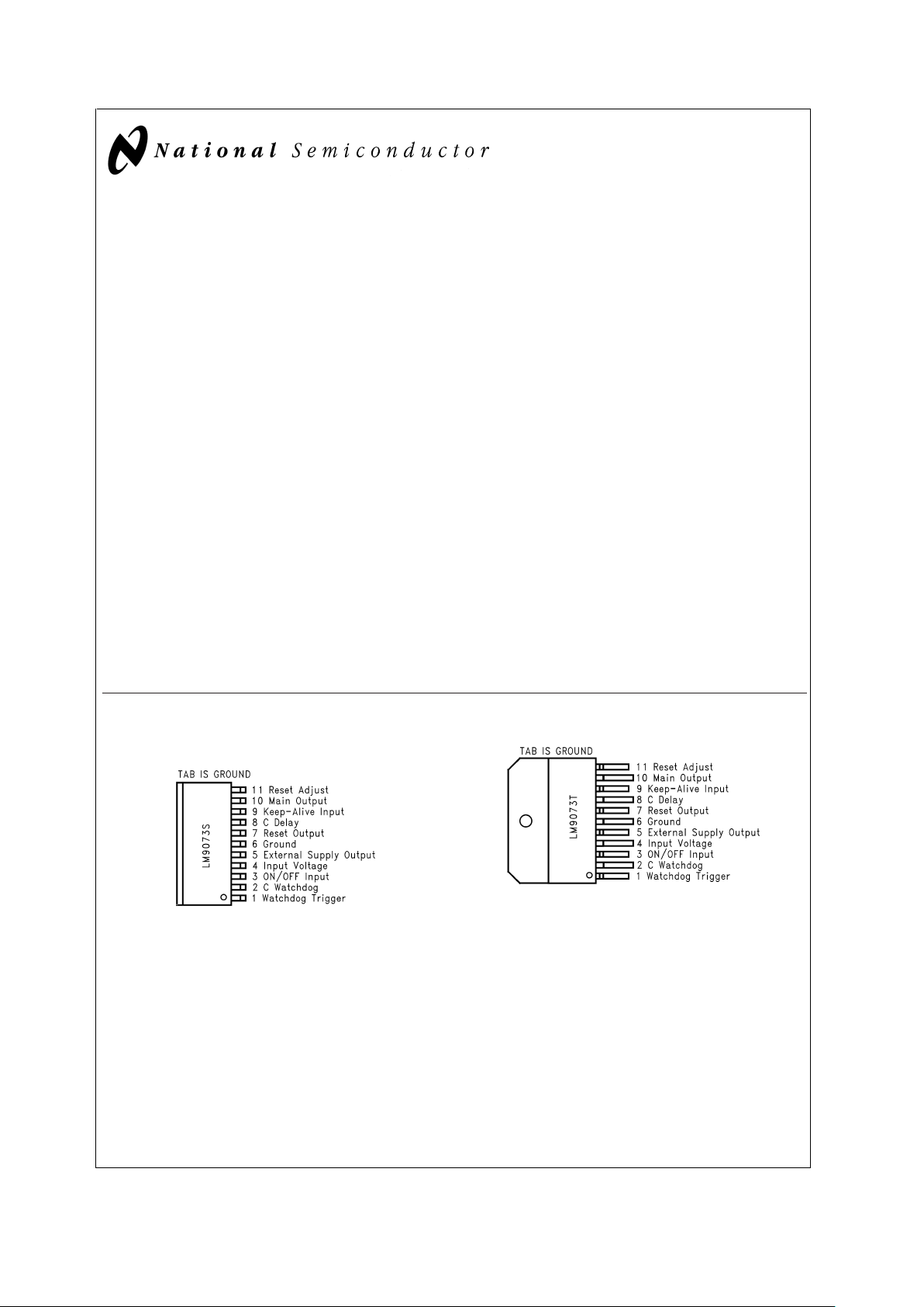
Connection Diagram
11 Lead TO−263 Package
DS101296-1
Top View
Order Number LM9073S
See NS Package Number TS11B
11 Lead TO−220 Package
DS101296-2
Top View
Order Number LM9073T
See NS Package Number TA11B
PRELIMINARY
April 2000
LM9073 Dual High Current Low-Dropout System Regulator
© 2000 National Semiconductor Corporation DS101296 www.national.com
Page 2
Block Diagram
DS101296-3
LM9073
www.national.com 2
Page 3
Absolute Maximum Ratings (Note 1)
If Military/Aerospace specified devices are required,
please contact the National Semiconductor Sales Office/
Distributors for availability and specifications.
Input Voltage −45V to 45V
Input Voltage (transient, t≤400mS) 60V
Forced Output Voltages
Main Output −0.3V to 7V
External Supply Output −0.3V to 27V
ON/OFF Input Voltage(Note 6) −0.3V to 16V
ON/OFF Input Current
±
20mA
Keep Alive In, Reset Out, C
DELAY
,
Reset Adjust,Watchdog Trigger
In, C Watchdog −0.3V to 7V
Junction Temperature 150˚C
Storage Temperature −65˚C to 150˚C
ESD Susceptibility(Note 2) 2000V
Lead temperature (Soldering, 10 Sec) 265˚C
Operating Ratings(Note 1)
Input Voltage Range 6V to 27V
Ambient Temperature Range −40˚C to 125˚C
Thermal Resistance
θ
JC
4˚C/W
θ
JA
43˚C/W
Electrical Characteristics
The following specifications apply for 6V ≤ vIN≤ 19V, t
CASE
= 25˚C unless otherwise specified. C
OUT
≥ 6µF with 0.3Ω≤ESR
≤ 0.3Ω on each regulator output.
Symbol Parameter Conditions
LM9073
Units
Min Max
MAIN REGULATOR
V
MAIN
Output Voltage
10mA ≤ I
LOAD
≤ 700mA 4.9 5.1 V
19V ≤ V
IN
≤ VSD,
5mA ≤ I
LOAD
≤ 700mA
4.8 5.2 V
R
MLOAD
Load Regulation
V
IN
= 16V, 10mA ≤ I
LOAD
≤
700mA
25 mV
R
MLINE
Line Regulation I
LOAD
= 700mA, 8V ≤ VIN≤ 16V 25 mV
V
MDO
Dropout Voltage, VIN−V
MAIN
V
IN
>
5.5V, 10mA ≤ I
LOAD
≤
700mA(Note 5)
1V
V
SD
Overvoltage Shutdown
Threshold
30 36 V
I
MSC
Output Short Circuit Current RL=1Ω 2000 mA
PSRR Ripple Rejection
V
IN
= 9V, 50Hz ≤ freq ≤ 20kHZ,
V
RIPPLE
=4V
P−P
40 dB
External Supply Regulator
V
EXT
Output Voltage 3mA ≤ I
LOAD
≤ 100mA 4.9 5.1 V
19V ≤ V
IN
≤ V
SD
3mA ≤ I
LOAD
≤ 100mA
4.8 5.2 V
R
ELOAD
Load Regulation
V
IN
= 16V, 3mA ≤ I
LOAD
≤
100mA
25 mV
R
ELINE
Line Regulation I
LOAD
= 100mA, 8V ≤ VIN≤ 16V 25 mV
V
EDO
Dropout voltage, VIN−V
EXT
V
IN
>
5.5V, 3mA ≤ I
LOAD
≤
100mA (Note 5)
0.8 V
V
SD
Overvoltage Shutdown
Threshold
30 36 V
I
ESC
Output Short Circuit Current RL=1Ω 250 mA
V
ESC
Output Short Circuit No effect on other functions −0.3 27 V
PSRR Ripple Rejection
V
IN
= 9V, 50Hz ≤ freq ≤ 20kHZ,
V
RIPPLE
=4V
PP
40 dB
Input Current
I
QOFF
Quiescent Input Current with
Both Regulators OFF.
8V ≤ V
IN
≤ 16V 100 µA
16V ≤ V
IN
≤ 42V 10 mA
I
Q
No Load Quiescent Current 8V ≤ VIN≤ 19V, IL= 0mA 15 mA
LM9073
www.national.com3
Page 4
Electrical Characteristics (Continued)
The following specifications apply for 6V ≤ vIN≤ 19V, t
CASE
= 25˚C unless otherwise specified. C
OUT
≥ 6µF with 0.3Ω≤ESR
≤ 0.3Ω on each regulator output.
Symbol Parameter Conditions
LM9073
Units
Min Max
Input Current
IN
ON
Additional Input Current with
both Regulators ON
V
IN
≥ 8V, I
LTOTAL=IMAIN
+
I
LEXT
I
LTOTAL
= 700mA + 100mA =
800mA
1.2
X
I
LTOTAL
LIN
DO
Additional Input Current when in
Dropout
0V
<
V
IN
<
8V, (Note 4)
I
LTOTAL=IMAIN+ILEXT
I
LTOTAL
= 700mA + 100mA =
800mA
1.5
X
I
LTOTAL
Reset Output
V
THRL
Low Switching Threshold
V
MAIN
output controls Reset
Reset Adjust (pin 11 )open
circuited
4.0 4.2 V
Reset Adjust (pin 11) shorted to
ground
4.5 4.7 V
V
THRH
High Switching Threshold V
MAIN
output controls Reset 5.35 5.75 V
V
LOW
Logic Low Output Threshold
1V ≤ V
MAIN
≤ V
THRL
R
RESET
= 50kΩ to V
MAIN
0.4 V
V
HIGH
Logic High Output Threshold
Normal opeation,
V
THRL
≤ V
MAIN≤THRH
,, I
SOURCE
=0
V
MAIN
−50mV
V
MAIN
V
R
P−U
Internal Pull-Up Resistance 2.4 6.0 kΩ
T
DELAY
Reset Delay Interval C
DELAY
= 0.1µF 35 70 mS
T
RISE
Output Rise Time
From 10% V
MAIN
to 90% V
MAIN
C
LRESET
= 50pF
1.5 µS
T
FALL
Output Fall Time
From 90% V
MAIN
to 10% V
MAIN
C
LRESET
= 50pF
0.5 µS
Watchdog
V
TRIGL
Trigger Input Logic Low Voltage .08 V
V
TRIGR
Trigger Input Logic High Level 2 V
T
WD
Watchdog Refresh Window
C
WATCHDOG
= 0.1µF (low
leakage)
I
WATCHDOG
for charging the
watchdog
35 70 mS
T
PW
Watchdog Trigger Pulse Width 10 µS
R
TRIG
Trigger Input Pull-down
Resistance
540kΩ
Control Inputs
V
ON
ON Threshold for ON/OFF Input Rseries = 22kΩ 3.5 4.5 V
V
OFF
OFF Threshold for ON/OFF
Inpu
Rseries = 22kΩ (Note 3) 1.5 2.5 V
I
ON/OFF
ON/OFF Input Current 1.4V ≤ V
ON/OFF
≤ 4.5V 1 12 µA
−0.3V ≤ V
ON/OFF
≤ 7V(Note 6) −1 5 mA
ON
K−A
Turn ON Threshold for Keep
Alive Input
2V
OFF
K−A
Turn OFF Threshold for Keep
Alive Input
(Note 3) 0.8 V
R
P−D
Pull−Down Resistance at Keep
Alive Input
0V ≤ V
K−A
≤ 5V 5 40 kΩ
LM9073
www.national.com 4
Page 5
Electrical Characteristics (Continued)
Note 1:
“Absolute Maximum Ratings”
indicate limits beyond which damage to the device may occur.
“Operating Ratings”
indicate conditions for which the device is
functional, but donot guaranteespecific performance limits.
“Electrical Characteristics”
state DC andAC electrical specificationsunder particulartest conditions which
guarantee specificperformance limits. This assumes that the device is within theOperating Ratings. Specifications are not guaranteed for parameters where no limit
is given, however, the typical value is a good indication of device performance.
Note 2: Human body model, 150 pFcapacitor discharged through a 1.5 kΩ resistor.
Note 3: If either control input is left open circuited the regulators will turn OFF.
Note 4: The input quiescent current will increase when the regulators are in dropout conditions. The amount of additional input current is a direct function of the to
a load current on both outputs. The peak increase in current is limited to 50% of the total load current.
Note 5: The dropoutvoltage specifications actually indicate the saturation voltage of the PNP power transistors used in eachregulator. Over the full load current and
temperature ranges the Main regulator will output at least 4.5V and the External Supply regulator at lease 4.7V with an input voltage of only 5.5V
Note 6: The ON/OFF input is internally clamped to a 7V zener diode through a 1KΩ resistor.
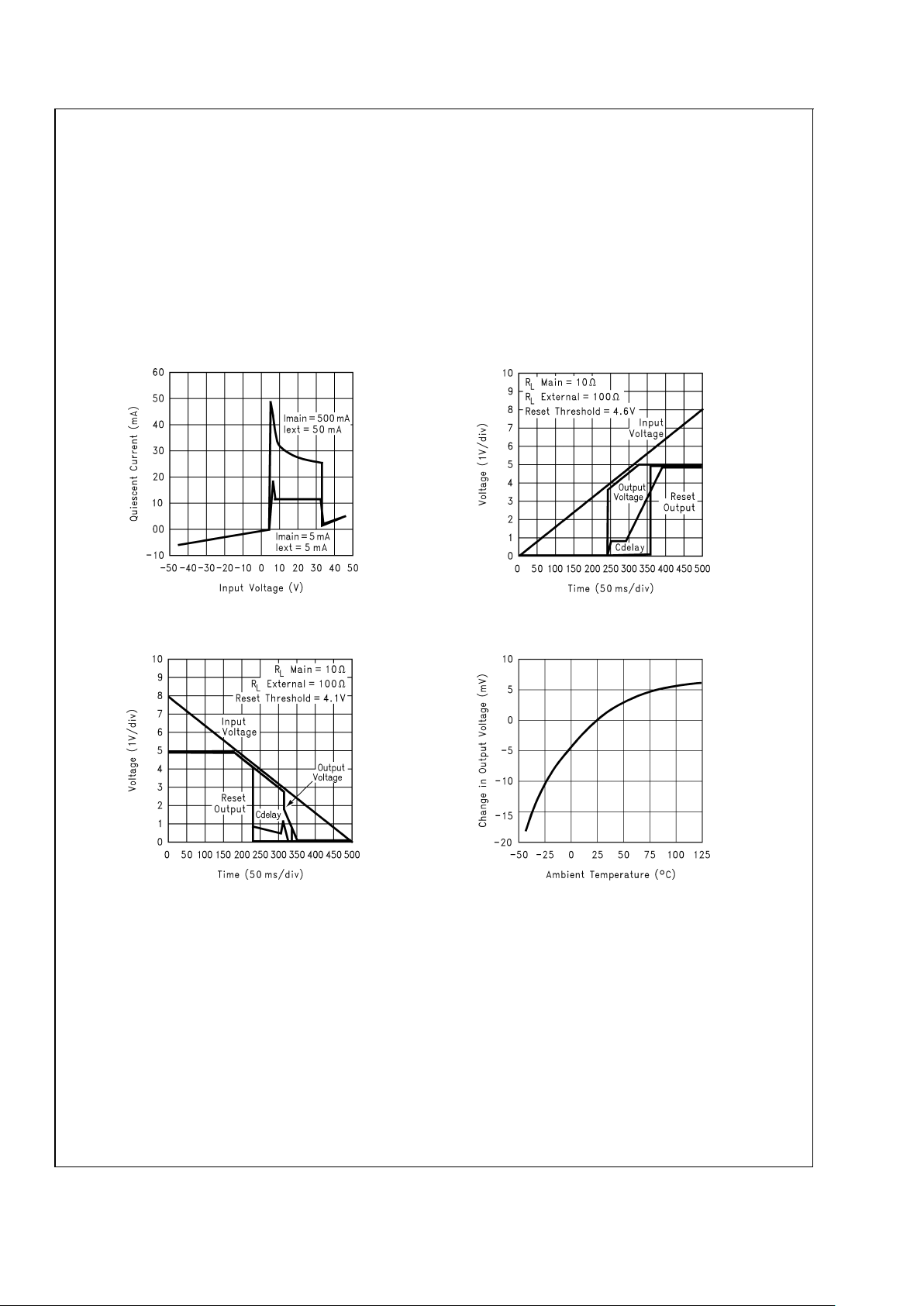
Quiescent Input Current vs. Input Voltage
DS101296-4
Turn-On Characteristic
DS101296-5
Turn-Off Characteristic
DS101296-6
Normalized Output Voltages vs Temperature
DS101296-7
LM9073
www.national.com5
Page 6
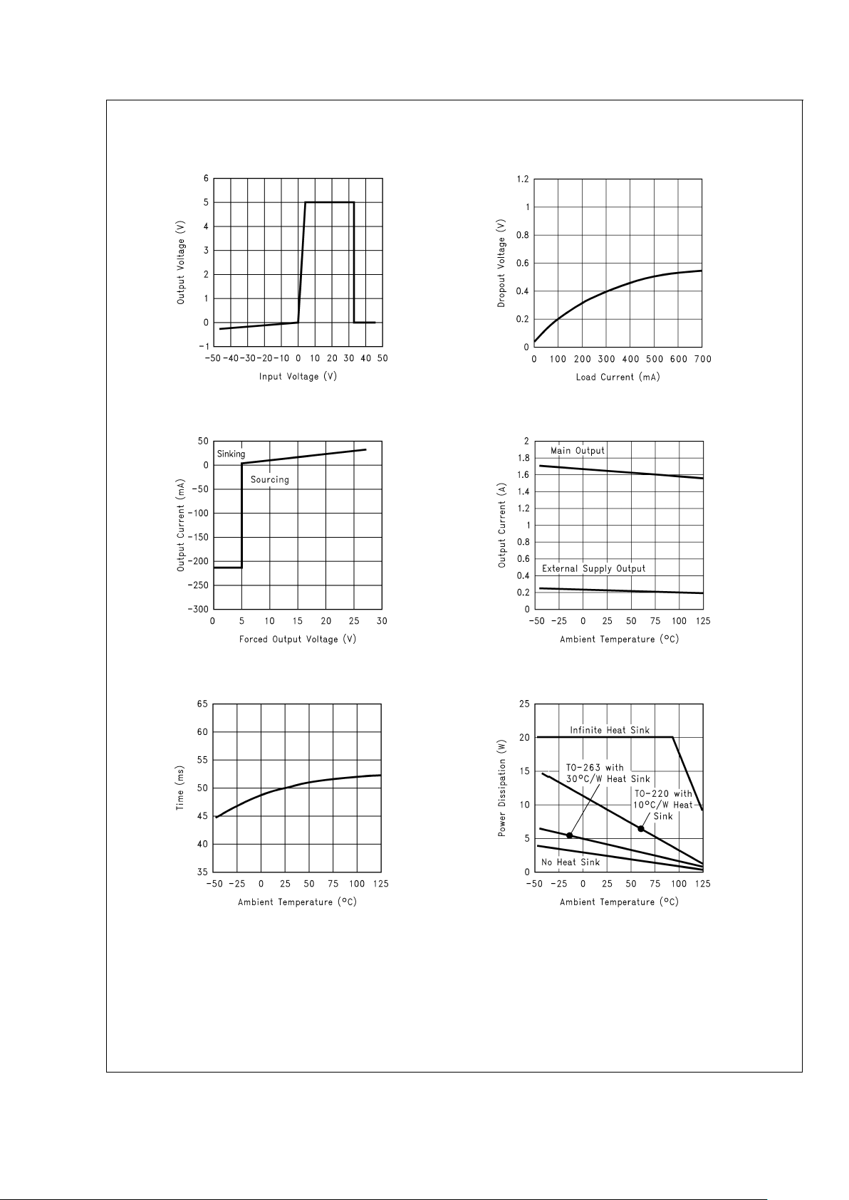
Electrical Characteristics (Continued)
Output Voltages at Input Voltage Extremes
DS101296-8
Main Output Dropout Voltage vs Load Current
DS101296-9
External Supply Output Short Circuit Current
DS101296-10
Output Short Circuit Current vs Temperature
DS101296-11
Watchdog and Reset Delay Time vs Temperature
DS101296-12
Maximum Power Dissipation
DS101296-13
LM9073
www.national.com 6
Page 7

Electrical Characteristics (Continued)
Output Capacitor ESR
DS101296-14
LM9073
www.national.com7
Page 8

Electrical Characteristics (Continued)
Operational Characteristics
DS101296-15
LM9073
www.national.com 8
Page 9

Control Logic Truth Table
ON/OFF Input Keep-Alive Input Main Output Voltage External Supply Output
Voltage
Reset Output Operating Condition
L L 0V 0V 0V OFF, Input curent
<
100µA
Rising Edge L 5V 5V Rising after delay
Outputs turn ON, Power ON
delayed reset
H X 5V 5V 5V Normal ON condition
HX
<
4V or
<
4.5V or
<
5.35V
X0V
Main output pulled out of
regulation,
Reset flag generated.
Threshold depends on Reset
Adjust seting (pin 11)
Falling Edge H 5V 5V 5V
Keep-Alive, Continued normal
operation
L Rising Edge 5V 5V Rising after delay
Outputs turned ON by
Keep-Alive Input
Application Information
Pin Description and Functionality
The LM9073 is a precision dual voltage regulator optimized
for use in powertrain module applications but will also find
use in a wide variety of automotive and industrial applications were precision supply regulation is required in harsh
operating environments. Thefollowing will describe the functionality of each of the package pins.
Input Voltage (pin 4)
The LM9073 has beendesignedto connect directly to the ignition or battery supply in automotive applications. For this
type ofsupply the regulator been designedto withstand up to
+60V and −45V supply transients such asload dump. An overvoltage shut down protection circuit turns OFF both of the
regulator outputs should supply transients exceed typically
+33V to fully protect all load circuitry. This higher threshold
allows normal operationwith 24V
DC
applied to theinput as in
the event when twobatteries are used to start a vehicle. Protection of the system is also provided for inadvertent reverse
polarity battery connections.
The current drain on the supply lineisdirectly proportional to
the load currents on the two voltage regulators. With no load
current on either output the regulator requires 15mA maximum quiescent current for biasing internal circuitry. During
dropout conditions (V
IN
<
5.5V) the additional input current
can rise to 50% of the total load current. With less than 3V
applied to the input, internal biasing circuitry shuts OFF.
When switched OFF the regulator can remain connected to
the battery supply with a current drain of less than 100µA.
Main Output (pin 10)
The Main Outputregulator provides a well controlled (2%tolerance maximum) 5V supply line with a total load current
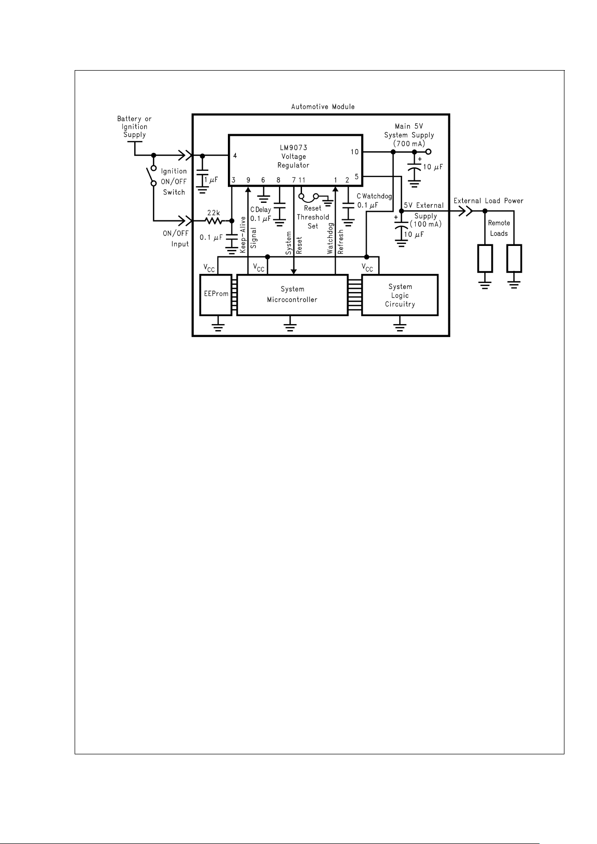
Figure 1. Circuit Block Diagram
DS101296-16
LM9073
www.national.com9
Page 10

Application Information (Continued)
ranging up to 700mA. This relatively high level of output current is sufficient to provide power to a large number of load
circuits in a variety of module applications.
This output has a short to ground current limit between
900mA and 2A. It is not protected for shorts to battery however, but can withstand an output short to a potential of 7
Volts or less.
To maintain stability of this supply line an output bypass capacitor is required. This capacitor must be at least 6µF with
an equivalent series resistance (ESR)between0.3Ω and 3Ω
over temperature.
The Main Output is sensed for the generation of the system
reset output.
External Supply Output (pin 5)
The External Supply Output regulator is a secondary 5V, 2%
tolerance regulated outputof the LM9073. this 100mAoutput
is available to bias sensors and other devices located external to the main system module.
For providing remote power the External Supply Output is
fully protected againstshort circuit connections to the battery
or input supply (up to 27V) and to ground. These shorted
fault conditions donot effect the operation ofthe main supply
nor generate a reset of the system.
Like the mainoutput a bypass capacitor isrequired for stability. This capacitor should be also greater than 6µF with an
ESR between 0.3Ω and 3Ω.
Reset Output (pin 7)
The Reset Output isan active low logic signal provided to reset a system mircocontroller on power up and in the event
that the Main Output falls out of regulation. This output is
guaranteed to provide a logic low level (
<
0.4V) whenever
the Main Output supplyis below a threshold set by the Reset
Adjust pin strapoption (see Reset Adjustsection)or is pulled
above 5.75V. This general reset prevents erratic system operation which may occur with out-of-specification supply potentials.
The Reset Output has an active pull down which can sink up
to 15mA of current and a passive pull-up (through a 4KΩ resistor) to the Main Output to ensure voltage compatibility
with the system supply. Capacitive loading on this reset line
will directly affect the rise time of the reset signal. The Reset
Output will maintain a logic low level with a MainOutput voltage of only 1V. Below 1V the active pull-down device
switches OFF (sink current of only 500µA). At such a low
supply potential, system controllers are generally inoperative.
The Reset Output has a built-in delay time interval which is
programmable by the section of the delay capacitor.
Reset Adjust (pin 11)
The low Vmain threshold voltage for generating a system reset can beshifted by 500mV through the use ofa pin strap to
ground on pin 11. With this pin shorted to ground the threshold is between 4.5V and 4.7V. With this pin left open the
threshold is shifted to between 4.0V and 4.2V. This lower
threshold allows the system to remain operational longer
during power down. The higher threshold ensures that the
system is reset when the nominal 5V supply is low by 10%,
which in some cases can produce uncertain microprocessor
operation.
Delay Capacitor (pin 8)
Figure 2. Reset Generator and Watchdog Circuitry
DS101296-17
LM9073
www.national.com 10
Page 11

Application Information (Continued)
The Delay Capacitor (C
DELAY
) controls a time interval during
which the Reset Output remains low after the Main Output
has established normal operating condition. This feature
holds the system in reset for a time to allow all load circuitry
to properly bias before executing functions. This interval is
applied atpower−up and following anyevent that may trigger
the system reset function.
Figure 2 illustrates the delayed reset generator. Two comparators continuallymonitor the Main Output supply. Window
comparators C1 and C2 detect if the Main Supply is below
4.6V (4.1V with Reset Adjust open circuited) or exceeds
5.5V typically. If this is true (at power−on for example) the
control logic turns ON the discharge transistor and holds
C
DELAY
low (at 0.9V). Comparator C4 then outputs a logic
low system Reset signal within 2µS after detecting the out of
regulation condition.
The Delay Capacitor remains discharged until the window
comparator senses that the Main Output is within normal operating range (C1 and C2 outputs are both low). When this
condition is met, the discharge transistor is turned OFF and
C
DELAY
is charged positively by an internal 6µA current
source. The Reset Output will remain low until the delay capacitor has reached 4V, at which point it will go high and the
system will begin normal operation. This delay time interval
is controlled bythe section of C
DELAY
and can bedetermined
from the following equation:
T
DELAY
= (0.5 x 10⁶)xC
DELAY
A 0.1µF capacitor will produce a typical delay interval of
50mSec.
To ensure a consistent delay time interval, the discharge
transistor is always latched ON by the window comparators,
and can not be switched OFF to start a new delay interval
until C
DELAY
has been discharged to less than or equal to
0.9V. This sets a fixed starting voltage (0.9V) and ending
voltage (4V) for the charging of the Delay Capacitor.
Watchdog Capacitor (pin 2)
The LM9073 also provides a simple system watchdog timer.
The watchdog timer requires the system controller to issue a
pulse at a regular interval (programmable through the selection of Cwatchdog)to provide an indication thatthe system is
properly executing controlling software code. The absence
of a pulse before the watchdog timer comes out could indicate that the system is caught in a infinite loop and the system is reset
The watchdog capacitor is held discharged to ground at any
time that the system is reset. When the reset is released the
capacitor quickly charges to 0.9V (with a charging current of
approximately 50µA) then slowly charges positive with a
charging current of 6µA. If this capacitor ever charges up to
4V or more, a system reset is generated.
The watchdog time intervalisset by the selection of Cwatchdog and can be found from the following equation:
T
WD
= (0.5 x 10⁶) x Cwatchdog
The watchdog timer function can be disabled by grounding
pin 2 or replacing Cwatchdog by a resistor with a value less
than 22kΩ. With this only the reset generator can reset the
system.
Watchdog Trigger (pin 1)
The WatchdogTrigger input acceptsa pulse from the system
controller to refresh the watchdog capacitor and prevent it
from reaching 4V and resetting the system. This positive
pulse must be at least 10µS long and triggers an internal
one-shot pulse. This internal pulse latches ON Qdischarge
Watchdog(figure 2) and discharges Cwatchdog to0.9V. This
latching action ensures a consistent watchdog timer interval
by not allowing the capacitor to charge positively until it has
been discharged to 0.9V.
As shown in Figure 3, each watchdog trigger input pulse resets the timer capacitor. If the watchdog trigger signal does
not refresh the timer before Cwatchdog reaches 4V, a system reset is generated. Once reset, a full reset delay interval
occurs. At the end of this interval the regulator will automatically try to re-startthe system by taking reset high. If the system does not respond properlybyissuing a watchdog trigger
signal in time, the system will once again reset. In this situation the reset output will continually cycle high (re-starting
the system) for the watchdog time interval and low
(re-setting the system) for the reset delay interval.
Figure 3. Watchdog and Reset Operation
DS101296-18
LM9073
www.national.com11
Page 12

Application Information (Continued)
Alow to high transition is required during the watchdog timer
interval at the trigger input. If this line is ever fixed high the
timer will time-out and the system will reset.
ON/OFF Input (pin 3)
The ON/OFF Input enables both the Main and External Supply outputs. In a typical application this input is connected to
the input supply through a series resistor (nominally 22KΩ)
and a switch (Ignition, as an example).When the switch is
closed this input is pulled high and switches ON both regulator outputs. This input is internally clamped to a 7V zener diode through a series 1kΩ resistor. The external series resistor together with an optional 0.1µF capacitor to ground
provide filtering and current limiting to withstand transients
that may appear on the input supply to maintain normal operation of the system.
The switching threshold of the ON/OFF comparator has 2
Voltsof hysteresis to ensure noisefree control of the system.
To turn the regulators ON this input must be taken above 4V.
To turn the system OFF the ON/OFF Input must be open circuited or pulled below 2 Volts.
Keep-Alive Input (pin 9)
This CMOS logic level compatible input provides a system
with the ability to control it’s own ON/OFF sequencing. The
Keep-Alive Input is OR’ed with the ON/OFF Input so either
one can independently control the regulators.
As shown in the Operational Characteristics, a system controller can take the Keep-Alive Input high at any time. If the
ON/OFF switch is opened, this high level on Keep-Alive will
keep the regulators ON and the entire system operational.
This control is useful for providing as much time as necessary for a system to perform ’housekeeping’ chores such as
programming EEPROM with system information prior to
turning itself OFF (by taking the Keep-Alive Input low) and
reverting to the low quiescent current state.
Asecond use of theKeep-Alive Input can befrom other modules which need information from the module powered by
LM9073. Ahigh CMOS logic level (
>
1.25V) on this input will
power up the system as needed independent from the normal ON/OFF switch.
System Keep-Alive Operation
Figure 5 illustrates the basic concept of Keep-Alive operation. The LM9073 provides the regulated supplies to an entire microcontroller based system or module including remote sensors. The system is switched ON or OFF by a
switch connected to the unregulated input supply and the
ON/OFF input, pin 3. When closed the regulators turn ON
and the system is held in a reset state for the duration of the
delayed reset interval controlled by C
DELAY
.
Once normal operation of the system begins, the controller
needs to set an output line connected to the Keep-Alive input, pin 9, high. The system remains in normal operation until switched OFF by opening the ON/OFF switch. With
Keep-Alive high the entire system remains normally biased
and willremain operational until the Keep-Aliveinput is taken
low.
Transistor Q1 is shown as a means to inform the controller
that the ON/OFF switch has been opened.This high level on
an input line tells the controller that the system has been
switched OFF. This indicates the start of the Keep-Alive interval. The system can perform whatever actions required to
obtain the proper OFF state before actually powering down.
These general housekeeping tasks can include putting external devices in the proper OFF condition and storing various system variables in EPROM for example. With the controller in command ofthe Keep-Alive interval these tasks can
take whatever time necessary to complete.
When completed the controller takes the Keep-Alive input to
a low level and the entire system shuts down. The LM9073
powers down to a low quiescent current mode with less than
100µA drawn from the input supply.
Figure 4. Remote ON/OFF Control
DS101296-19
LM9073
www.national.com 12
Page 13

Application Information (Continued)
To initiate the Keep-Alive routine before actual power down,
it isimportant for the system controllerto know when thesystem has been switched OFF. To eliminate any interface between the controller and the ON/OFF switch and potentially
noisy unregulated input supply, and simple logic scheme
shown in Figure 6 can be used. With this circuitry the Reset
output form the LM9073 provides the ON/OFF sensing input
to the controller.
When switched OFF, the main regulator output will fall out of
regulation and generate a low logic level on the Reset output. This input to the controller provides the switch OFF indication and initiates the Keep-Alive interval.
Control of the Keep-Alive duration is set by a logic 1 on the
Keep-Alive output line from the system controller. This high
level prevents the Reset output from resetting the entire system and also gates the Keep-Alive input signal to the
LM9073. The inverted Reset signal provides a logic 1 to the
Keep-Alive input of the LM9073.
The Main output will only drop out of regulation for a very
short time before the Keep-Alive input turns it back on.
The Reset output remains low for the delay time interval.
When it turns high the Main output switches OFF and back
ON again very quickly. This continues until the system controller takes the Keep-Alive output line to a logic low level.
Figure 5. Basic Keep-Alive Operation
DS101296-20
LM9073
www.national.com13
Page 14

Application Information (Continued)
Input Stability
Low dropout voltage regulators which utilize a PNP power
transistor usually exhibit a large increase in current when in
dropout (Vin
<
5.5V). This increase is caused by the saturation characteristics (β reduction) of the PNP transistor. To
significantly minimize this increase in current the LM9073
detects when the PNP enters the saturation and reduces the
operating current.
This reduction in input current can create a stability problem
in applications withhigher load current (
>
200mA). where the
input voltage isapplied through a long length ofwire which in
effect add a significant amount of inductance in series with
the input. The drop in input current may create a positive input voltage transient which may take the PNP out of saturation. If the input voltage is held constant at the threshold
where the PNP is going in and out of saturation, an oscillation may be created.
This is only observed where a large series inductance is
present in the input supply line and when the rise and fall
time of theinputsupply is very slow.If the application and removal of the input voltage changes at a rate greater than
500mV/mS it will move through the dropout region of the
regulator (Vin of 3V to 5.5V) too quickly for an oscillation to
be established.
Figure 6. Simple Logic Configuration to Provide
ON/OFF Sensing
DS101296-21
LM9073
www.national.com 14
Page 15

Application Information (Continued)
In the event that an oscillation is present, input bypassing
can also help de-tune the resonance. Figure 7 illustrates two
input bypassing approaches.The straight forward addition of
a larger valued electrolitic capacitor could suffice. In this
case however,if reverse battery connections arepossibility it
is necessary to add a series protection diode as shown to
prevent damaging the polarized input capacitor.
An alternative input bypassing scheme is also shown. This
eliminates the use of polarized input capacitors and a series
protection diode. The values shown were derivedempirically
in a representative typical application.Appropriate values for
any given application require experimentation.
Thermal Management
The LM9073 is packaged in both a TO-263 surface mount
power package and anarrowlead-pitch TO-220 package. To
obtain operation over the highest possible load current and
input voltage ranges, care must be taken to control the operating temperature of the device. Thermal shutdown protection is built with a threshold above 150˚C Conventional heat
sinking techniques can be used with the TO-220 package.
When applying theTO-263 package on-board heatsinking is
important to prevent thermal shutdown. More copper foil
area under the tab ofthe device will directly reduce the operating junction temperature. Use of a double sided board with
vias between two planes of copper as shown in Figure 8 will
improve performance ad can optimize the PC board surface
area required.
Figure 7. Input Bypassing
DS101296-22
Figure 8. Typical TO-263 PC Board Heatsinking
DS101296-23
LM9073
www.national.com15
Page 16

Application Information (Continued)
Electro-Magnetic Compatibiltiy (EMC)
Systems utilizing theLM9073 will not experience loss ofsupply or false reset signals from the regulator when subjected
to high frequency interference from a standard Bulk Current
Injection test (ISO11452 Part 4 test method). The following
test conditions and configuration (Figure 9) can be used to
verify this performance:
•
Frequency Range 1MHz to 400MHz
•
Modulation 1 (no modulation)
•
Modulation 2 1kHz sine wave, 80% AM
•
Dwell Time 1 second
•
Frequency Steps 1MHz (from 1MHz to 10MHz)
•
2MHz (from 10MHz to 200MHz)
•
20MHz (from 200MHz to 400MHz)
•
Test Method Closed loop current probe
In this test configuration the current injected in to either the
input pin or the tracking output pin is increased until a reset
output is generated. These two pins are the most critical as
they typically will connect to a module through long lengths
of wire most likely to pick up high frequency energy. Figure
10 illustrates examples of test results on the LM9073 with
both types of modulation.
These results are just examples as actual results in any
given application will depend on numerous external factors
such as component selection, pc board layout, etc. The current power ofthe injected signal is expressed indB relativeto
1mA (i.e. 40dBmA = 100mA)
Figure 9. EMC Test Circuit
DS101296-24
Figure 10. Examples of BCI Test
BCI Susceptibility, Modulation 1 (CW)
DS101296-25
BCI Susceptibility, Modulation 2 (CW)
(1kHz, 80% AM Modulation)
DS101296-26
LM9073
www.national.com 16
Page 17

Physical Dimensions inches (millimeters) unless otherwise noted
Order Number LM9073S
NS Package Number TS11B
LM9073
www.national.com17
Page 18

Physical Dimensions inches (millimeters) unless otherwise noted (Continued)
LIFE SUPPORT POLICY
NATIONAL’S PRODUCTS ARE NOT AUTHORIZED FOR USE AS CRITICAL COMPONENTS IN LIFE SUPPORT
DEVICES OR SYSTEMS WITHOUT THE EXPRESS WRITTEN APPROVAL OF THE PRESIDENT AND GENERAL
COUNSEL OF NATIONAL SEMICONDUCTOR CORPORATION. As used herein:
1. Life support devices or systems are devices or
systems which, (a) are intended for surgical implant
into the body, or (b) support or sustain life, and
whose failure to perform when properly used in
accordance with instructions for use provided in the
labeling, can be reasonably expected to result in a
significant injury to the user.
2. A critical component is any component of a life
support device or system whose failure to perform
can be reasonably expected to cause the failure of
the life support device or system, or to affect its
safety or effectiveness.
National Semiconductor
Corporation
Americas
Tel: 1-800-272-9959
Fax: 1-800-737-7018
Email: support@nsc.com
National Semiconductor
Europe
Fax: +49 (0) 180-530 85 86
Email: europe.support@nsc.com
Deutsch Tel: +49 (0) 69 9508 6208
English Tel: +44 (0) 870 24 0 2171
Français Tel: +33 (0) 1 41 91 8790
National Semiconductor
Asia Pacific Customer
Response Group
Tel: 65-2544466
Fax: 65-2504466
Email: ap.support@nsc.com
National Semiconductor
Japan Ltd.
Tel: 81-3-5639-7560
Fax: 81-3-5639-7507
www.national.com
Order Number LM9073T
NS Package Number TA11B
LM9073 Dual High Current Low-Dropout System Regulator
National does not assume any responsibility for use of any circuitry described, no circuit patent licenses are implied and National reserves the right at any time without notice to change said circuitry and specifications.
 Loading...