

Page 1
LM9071
Low-Dropout System Voltage Regulator with Delayed
Reset
General Description
The LM9071 is a 5V, 250 mAlow-dropout voltage regulator.
The regulator features an active low delayed reset output
flag which can be used to reset a microprocessor system on
turn-ON and in the event that the regulator output falls out of
regulation for any reason. An external capacitor programs a
delay time interval before the reset output can return high.
Designed for automotive application the LM9071 contains a
variety of protection features such as reverse battery,
over-voltage shutdown, thermal shutdown, input transient
protection and a wide operating temperature range.
Design techniques have been employed to allow the regulator to remain operational and not generatefalse resetsignals
when subjected to high levels of RF energy (300V/m from
2 MHz to 400 MHz).
Features
n Automotive application reliability
n 3%output voltage tolerance
n Insensitive to radiated RFI
n Dropout voltage less than 800 mV with 250 mA output
current
n Externally programmed reset delay interval
n Thermal shutdown
n Short circuit protection
n Reverse battery protection
n Wide operating temperature range −40˚C to +125˚C
n TO-220 and TO-263 power surface mount power
packages
n Pin for pin compatible with the LM2927, L4947 and
TLE4260
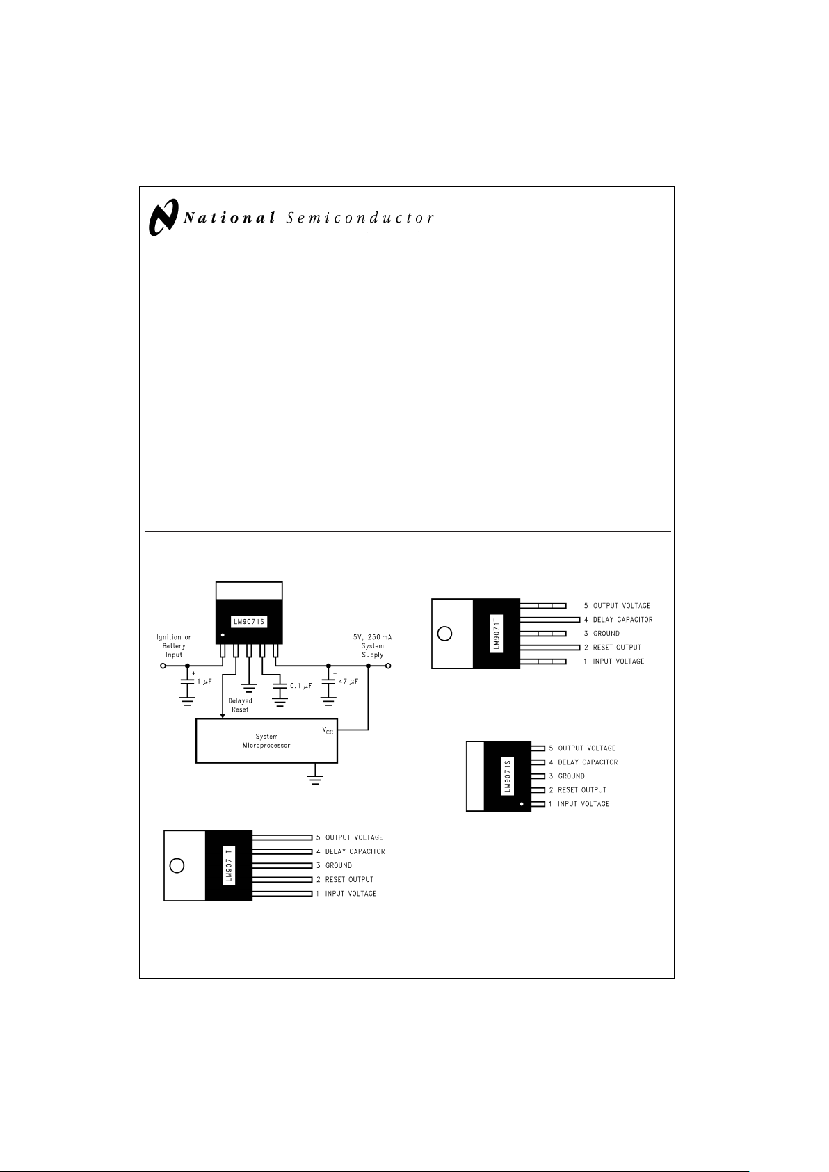
Typical Application and Connection Diagrams (Top View)
DS012832-1
5-Lead TO-220 Package
DS012832-2
Order Number LM9071T
See NS Package Number T05A
5-Lead TO-220 Package
DS012832-3
Order Number LM9071T/Flow LB03
See NS Package Number T05D
5-Lead TO-263 Surface Mount Package
DS012832-4
Tab and Backside metal on all packages internally connected to ground.
Order Number LM9071S
See NS Package Number TS5B
December 1999
LM9071 Low-Dropout System Voltage Regulator with Delayed Reset
© 1999 National Semiconductor Corporation DS012832 www.national.com
Page 2
Absolute Maximum Ratings (Note 1)
DC Input Voltage −26V to +26V
Positive Input Transient (t
<
100 ms) 60V
Negative Input Transient (t
<
1 ms) −50V
Reset Output Sink Current 5 mA
Power Dissipation Internally Limited
Junction Temperature 150˚C
ESD Susceptibility (Note 2) 12 kV, 2 kV
Lead Temperature
(Soldering, 10 seconds) 260˚C
Storage Temperature −50˚C to +150˚C
Operating Ratings (Note 1)
Input Voltage 6V to 26V
Ambient Temperature −40˚C to +125˚C
θjc, TO-220, TO-263 Packages 3˚C/W
θja, TO-220, TO-263 Packages 43˚C/W
Electrical Characteristics
The following specifications apply for V
CC
=
6V to 26V, −40˚C ≤ T
A
≤+125˚C, unless otherwise specified. C
OUT
=
47 µFd with
an ESR
<
3Ω.C
IN
=
1 µFd.
Symbol Parameter Conditions Min Max Units
REGULATOR OUTPUT
V
OUT
Output Voltage 5 mA ≤ I
OUT
≤ 250 mA 4.85 5.15 V
∆V
OUT
Line Line Regulation I
OUT
=
5 mA, 9V ≤ V
IN
≤ 16.5V 25 mV
I
OUT
=
250 mA 50 mV
∆V
OUT
Load Load Regulation V
IN
=
14.4V, 5 mA ≤ I
OUT
≤ 250 mA 60 mV
Iq Quiescent Current I
OUT
=
5mA 4 mA
I
OUT
=
250 mA, V
IN
≥ 8V 25 mA
I
OUT
=
5 mA, V
IN
=
5V 10 mA
I
OUT
=
250 mA, V
IN
=
6V 50 mA
Vdo Dropout Voltage I
OUT
=
5 mA 300 mV
I
OUT
=
250 mA 800 mV
Isc Short Circuit Current R
L
=
1Ω 0.35 1.5 A
RR Ripple Rejection F
ripple
=
120 Hz, V
ripple
=
1 Vrms
I
OUT
=
50 mA
60 dB
OVthr Overvoltage Shutdown
Threshold
27 V
V
O
Transient V
OUT
during Transients VINPeak ≤ 60V, R
L
=
100Ω, τ=100 ms 7 V
RESET OUTPUT
Vth Threshold Voltage ∆V
OUT
Required to Generate a Reset
Output
4.8V ≤ V
OUT
≤ 5.2V
−300 −500 mV
Vlow Reset Output Low Voltage Isink=1.6 mA, V
OUT
>
3.2V 0.4 V
1.4V ≤ V
OUT
≤ 3.2V 0.8 V
Vhigh Reset Output High Voltage 0.8
V
OUT
V
t
delay
Delay Time Cdelay=100 mFd 7.6 35 ms
Idelay Charging Current for Cdelay 10 30 µA
Rpu Internal Pull-up Resistance 12 80 kΩ
Note 1: Absolute Maximum Ratings indicate limits beyond which damage to the device may occur. Operating Ratings indicate conditions for which the device is
intended to be functional, but do not guarantee specific performance limits. For guaranteed specifications and conditions, see the Electrical Characteristics.
Note 2: All pins will survive an ESD impulse of
±
2000V using the human body model of 100 pF discharged through a 1.5 kΩ resistor. In addition the input voltage
pin will withstand ten pulses of
±
12 kV from a 150 pF capacitor discharged through a 560Ω resistor when bypassed with a 22 nF, 100V capacitor.
LM9071
www.national.com 2
Page 3
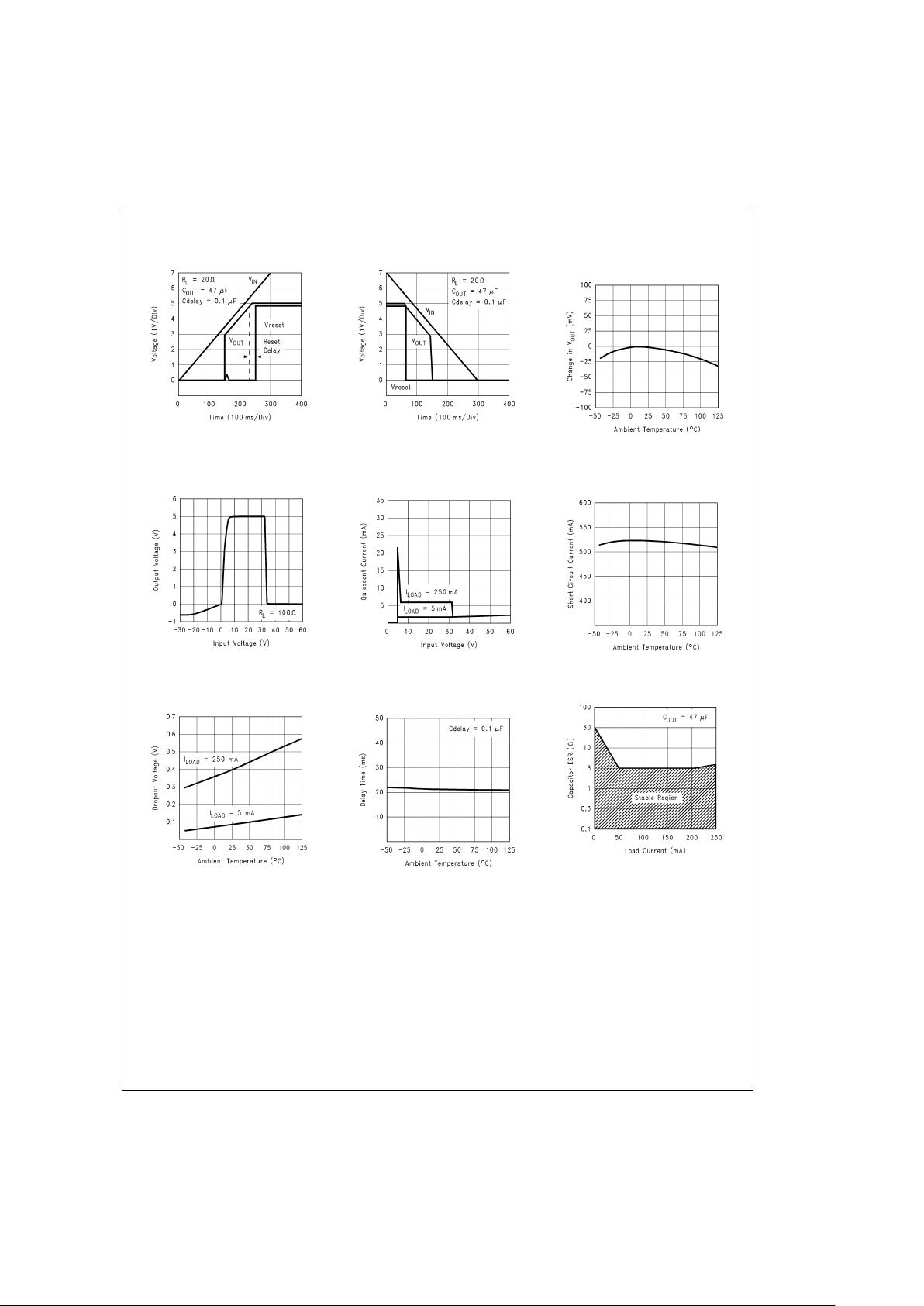
Typical Performance Characteristics (T
A
=
25˚C unless indicated otherwise)
Turn ON Characteristics
DS012832-5
Turn OFF Characteristics
DS012832-6
Normalized Output Voltage
vs Temperature
DS012832-7
Output Voltage at
Input Voltage Extremes
DS012832-8
Quiescent Current vs
Input Voltage
DS012832-9
Short Circuit Current
vs Temperature
DS012832-10
Dropout Voltage vs
Temperature
DS012832-11
Reset Delay Time
vs Temperature
DS012832-12
Output Capacitor ESR
DS012832-13
LM9071
www.national.com3
Page 4

Typical Performance Characteristics (T
A
=
25˚C unless indicated otherwise) (Continued)
Reset Operation and Protection Features
Block Diagram
Maximum Power Dissipation
(TO-220 Package)
DS012832-14
Maximum Power Dissipation
(TO-263 Package)
DS012832-15
DS012832-16
DS012832-17
LM9071
www.national.com 4
Page 5

Application Hints
The LM9071 voltage regulator has been optimized for use in
microprocessor based automotive systems. Several unique
design features have been incorporated to address many
FMEA (Failure Mode Effects Analysis) concerns for fail-safe
system performance.
FAULT TOLERANT FEATURES
While not specifically guaranteed due to production testing
limitations, the LM9071 has been tested and shown to continue to provide a regulated output and, not generate an erroneous system reset signal while subjected to high levels of
RF electric field energy (up to 300 V/m signal strength over
a 2 MHz to 400 MHz frequency range). This is very important
in vehicle safety related applications where the system must
continue to operate normally. To maintain this immunity to
RFI the output bypass capacitor is important (47 µF is recommended).
An output bypass capacitor of at least 10 µF is required for
stability (47 µF is recommended). The ESR of this capacitor
should be less than 3Ω. An input capacitor of 1 µF or larger
is recommended to improve line transient and noise performance.
Conventional load dump protection is built in to withstand up
to +60V and −50V transients. Protection against reverse polarity battery connections is also built in. Witha reversed battery connection the output of the LM9071 will not go more
negative than one diode drop below ground.This willprevent
damage to any of the 5V load circuits.
RESET FLAG
Excessive loading of the output to the point where the output
voltage drops by 300 mV to 500 mV will signal a reset flag to
the micro. This will warn of a V
CC
supply that may produce
unpredictable operation of the system. On power-up and re-
covery from a fault condition the delay capacitor is used to
hold the micro in a reset condition for a programmable time
interval to allow the system operating voltages and clock to
stabilize before executing code. The delay time interval can
be estimated by the following equation:
INPUT STABILITY
Low dropout voltage regulators which utilize a PNP power
transistor usually exhibit a large increase in current when in
dropout (V
IN
<
5.5V). This increase is caused by the saturation characteristics (β reduction) of the PNP transistor. To
significantly minimize this increase in current the LM9071
detects when the PNP enters saturation and reduces the operating current.
This reduction in input current can create a stability problem
in applications with higher load current (
>
100 mA) where
the input voltage is applied through a long length of wire,
which in effect adds a significant amount ofinductance in series with the input. The drop in input current may create a
positive input voltage transient which may take the PNP out
of saturation. If the input voltage is held constant at the
threshold where the PNP is going in and out of saturation, an
oscillation may be created.
This is only observed where a large series inductance is
present in the input supply line and when the rise and fall
time of the input supply isvery slow.If the application and removal of the input voltage changes at a rate greater than
500 mV/µs it will move through the dropout region of the
regulator (V
IN
of 3V to 5.5V) too quickly for an oscillation to
be established.
LM9071
www.national.com5
Page 6

Physical Dimensions inches (millimeters) unless otherwise noted
5-Lead Molded TO-220
Order Number LM9071T
NS Package Number T05A
5-Lead Molded TO-220
Order Number LM9071T/Flow LB03
NS Package Number T05D
LM9071
www.national.com 6
Page 7

Physical Dimensions inches (millimeters) unless otherwise noted (Continued)
LIFE SUPPORT POLICY
NATIONAL’S PRODUCTS ARE NOT AUTHORIZED FOR USE AS CRITICAL COMPONENTS IN LIFE SUPPORT
DEVICES OR SYSTEMS WITHOUT THE EXPRESS WRITTEN APPROVAL OF THE PRESIDENT AND GENERAL
COUNSEL OF NATIONAL SEMICONDUCTOR CORPORATION. As used herein:
1. Life support devices or systems are devices or
systems which, (a) are intended for surgical implant
into the body, or (b) support or sustain life, and
whose failure to perform when properly used in
accordance with instructions for use provided in the
labeling, can be reasonably expected to result in a
significant injury to the user.
2. A critical component is any component of a life
support device or system whose failure to perform
can be reasonably expected to cause the failure of
the life support device or system, or to affect its
safety or effectiveness.
National Semiconductor
Corporation
Americas
Tel: 1-800-272-9959
Fax: 1-800-737-7018
Email: support@nsc.com
National Semiconductor
Europe
Fax: +49 (0) 1 80-530 85 86
Email: europe.support@nsc.com
Deutsch Tel: +49 (0) 1 80-530 85 85
English Tel: +49 (0) 1 80-532 78 32
Français Tel: +49 (0) 1 80-532 93 58
Italiano Tel: +49 (0) 1 80-534 16 80
National Semiconductor
Asia Pacific Customer
Response Group
Tel: 65-2544466
Fax: 65-2504466
Email: sea.support@nsc.com
National Semiconductor
Japan Ltd.
Tel: 81-3-5639-7560
Fax: 81-3-5639-7507
www.national.com
5-Lead Molded TO-263
Order Number LM9071S
NS Package Number TS5B
LM9071 Low-Dropout System Voltage Regulator with Delayed Reset
National does not assume any responsibility for use of any circuitry described, no circuit patent licenses are implied and National reserves the right at any time without notice to change said circuitry and specifications.
 Loading...