

Page 1
TL/H/12317
LM9061 Power MOSFET Driver with Lossless Protection
April 1995
LM9061
Power MOSFET Driver with Lossless Protection
General Description
The LM9061 is a charge-pump device which provides the
gate drive to any size external power MOSFET configured
as a high side driver or switch. A CMOS logic compatible
ON/OFF input controls the output gate drive voltage. In the
ON state, the charge pump voltage, which is well above the
available V
CC
supply, is directly applied to the gate of the
MOSFET. A built-in 15V zener clamps the maximum gate to
source voltage of the MOSFET. When commanded OFF a
110 mA current sink discharges the gate capacitances of
the MOSFET for a gradual turn-OFF characteristic to minimize the duration of inductive load transient voltages and
further protect the power MOSFET.
Lossless protection of the power MOSFET is a key feature
of the LM9061. The voltage drop (V
DS
) across the power
device is continually monitored and compared against an
externally programmable threshold voltage. A small current
sensing resistor in series with the load, which causes a loss
of available energy, is not required for the protection circuitry. Should the V
DS
voltage, due to excessive load current,
exceed the threshold voltage, the output is latched OFF in a
more gradual fashion (through a 10 mA output current sink)
after a programmable delay time interval.
Designed for the automotive application environment the
LM9061 has a wide operating temperature range of
b
40§C
to
a
125§C, remains operational with VCCup to 26V, and
can withstand 60V power supply transients. The LM9061 is
available in an 8-pin small outline package, and an 8-pin
dual in-line package.
Features
Y
Built-in charge pump for gate overdrive of high side
drive applications
Y
Lossless protection of the power MOSFET
Y
Programmable MOSFET protection voltage
Y
Programmable delay of protection latch-OFF
Y
Fast turn-ON (1.5 ms max with gate capacitance of
25000 pF)
Y
Undervoltage shut OFF with V
CC
k
7V
Y
Overvoltage shut OFF with V
CC
l
26V
Y
Withstands 60V supply transients
Y
CMOS logic compatible ON/OFF control input
Y
Surface mount and dual in-line packages available
Applications
Y
Valve, relay and solenoid drivers
Y
Lamp drivers
Y
DC motor PWM drivers
Y
Logic controlled power supply distribution switch
Y
Electronic circuit breaker
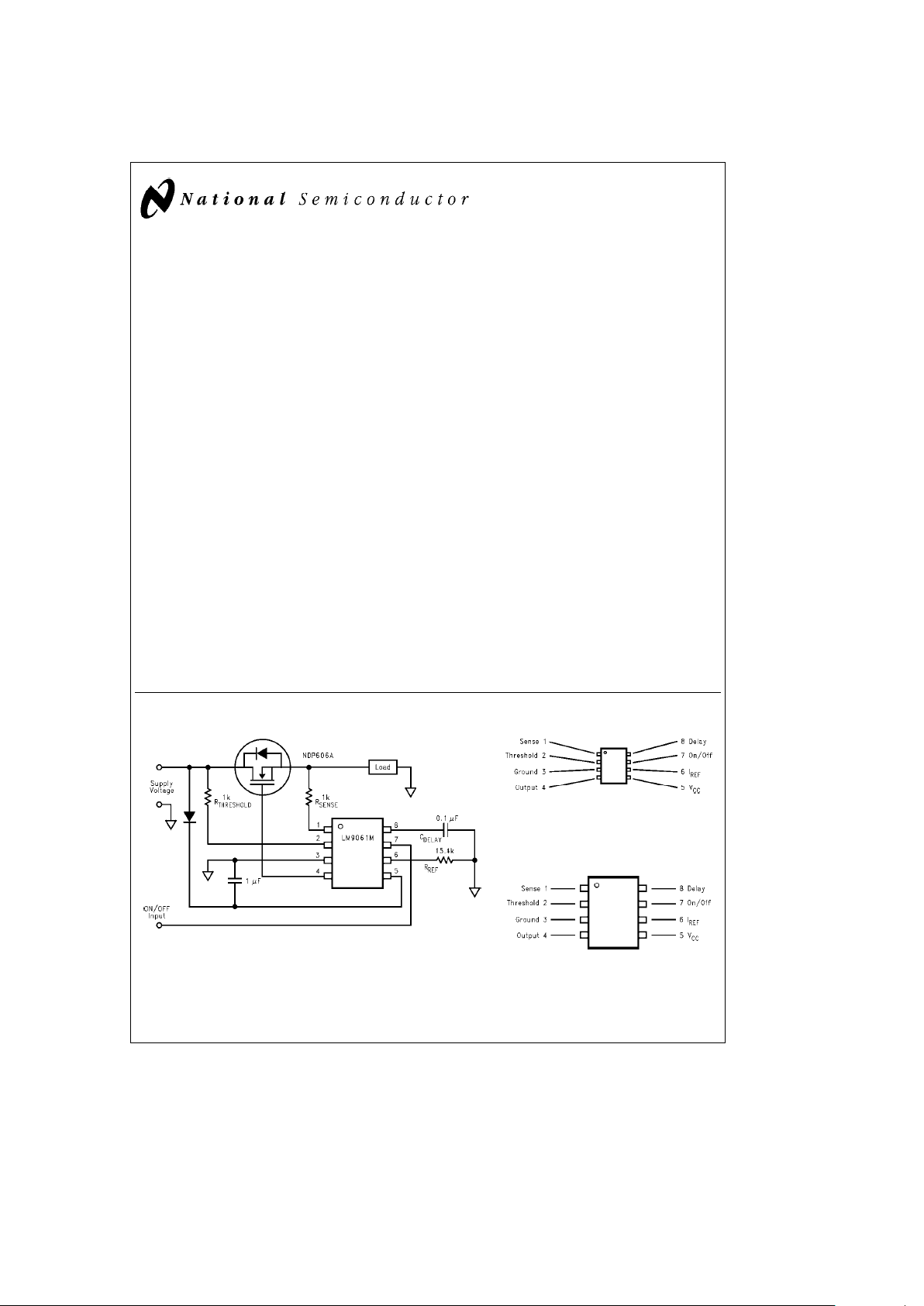
Typical Application
TL/H/12317– 1
Connection Diagrams
TL/H/12317– 3
Top View
Order Number LM9061M
See NS Package Number M08A
TL/H/12317– 2
Top View
Order Number LM9061N
See NS Package Number N08E
C
1995 National Semiconductor Corporation RRD-B30M115/Printed in U. S. A.
Page 2
Absolute Maximum Ratings (Note 1)
If Military/Aerospace specified devices are required,
please contact the National Semiconductor Sales
Office/Distributors for availability and specifications.
Supply Voltage 60V
Reverse Supply Current 20 mA
Output Voltage V
CC
a
15V
Voltage at Sense and Threshold
(through 1 kX)
b
25V toa60V
ON/OFF Input Voltage
b
0.3V to V
CC
a
0.3V
Junction Temperature 150§C
Storage Temperature
b
55§Cto150§C
Lead Temperature (Soldering, 10 seconds) 260
§
C
Operating Ratings (Note 2)
Supply Voltage 7V to 26V
ON/OFF Input Voltage
b
0.3V to V
CC
Ambient Temperature Range
b
40§Cto125§C
Thermal Resistance (i
J-A
)
LM9061M 150§C/W
LM9061N 100
§
C/W
DC Electrical Characteristics
7VsV
CC
s
20V, R
REF
e
15.4 kX,b40§CsT
J
s
a
125§C, unless otherwise specified.
Symbol Parameter Conditions Min Max Units
POWER SUPPLY
I
Q
Quiescent Supply Current ON/OFFe‘‘0’’ 5 mA
I
CC
Operating Supply Current ON/OFFe‘‘1’’,
C
LOAD
e
0.025 mF,
40 mA
Includes Turn-ON
Transient Output Current
ON/OFF CONTROL INPUT
VIN(0) ON/OFF Input Logic ‘‘0’’ V
OUT
e
OFF 1.5 V
VIN(1) ON/OFF Input Logic ‘‘1’’ V
OUT
e
ON 3.5 V
V
HYST
ON/OFF Input Hysteresis Peak to Peak 0.8 2 V
I
IN
ON/OFF Input Pull-Down Current VON/OFFe5V 50 250 mA
GATE DRIVE OUTPUT
V
OH
Charge Pump Output Voltage ON/OFFe‘‘1’’ V
CC
a
7V
CC
a
15 V
V
OL
OFF Output Voltage ON/OFFe‘‘0’’,
0.9 V
I
SINK
e
110 mA
V
CLAMP
Sense to Output ON/OFFe‘‘1’’,
11 15 V
Clamp Voltage V
SENSE
e
V
THRESHOLD
I
SINK(Normal-OFF)
Output Sink Current, ON/OFFe‘‘0’’,
Normal Operation V
DELAY
e
0V, 75 145 mA
V
SENSE
e
V
THRESHOLD
I
SINK(Latch-OFF)
Output Sink Current with V
DELAY
e
7V,
515mA
Protection Comparator Tripped V
SENSE
k
V
THRESHOLD
PROTECTION CIRCUITRY
I
REF
Threshold Pin Reference Current V
SENSE
e
V
THRESHOLD
75 88 m A
V
REF
Reference Voltage 1.15 1.35 V
I
THR(LEAKAGE)
Threshold Pin Leakage Current V
CC
e
Open,
10 mA
7V
s
V
THRESHOLD
s
20V
I
SENSE
Sense Pin Input Bias Current V
SENSE
e
V
THRESHOLD
10 mA
DELAY TIMER
I
DELAY
Delay Pin Source Current 6.74 15.44 mA
V
TIMER
Delay Timer Threshold Voltage 5 6.2 V
I
DIS
Delay Capacitor Discharge Current V
DELAY
e
5V 2 10 mA
V
SAT
Discharge Transistor Saturation Voltage I
DIS
e
1 mA 0.4 V
2
Page 3
AC Timing Characteristics
7VsV
CC
s
20V, R
REF
e
15.4 kX,b40§CsT
J
s
a
125§C, C
LOAD
e
0.025 mF, C
DELAY
e
0.022 mF, unless otherwise
specified.
Symbol Parameter Conditions Min Max Units
T
ON
Output Turn-ON Time C
LOAD
e
0.025 mF
7V
s
V
CC
s
10V, V
OUT
t
V
CC
a
7V 1.5 ms
10V
s
V
CC
s
20V, V
OUT
t
V
CC
a
11V 1.5 ms
T
OFF(Normal)
Output Turn-OFF Time, C
LOAD
e
0.025 mF
Normal Operation V
CC
e
14V, V
OUT
t
25V 4 10 ms
(Note 4) V
SENSE
e
V
THRESHOLD
T
OFF(Latch-OFF)
Output Turn-OFF Time, C
LOAD
e
0.025 mF
Protection Comparator Tripped V
CC
e
14V, V
OUT
t
25V 45 140 ms
(Note 4) V
SENSE
e
V
THRESHOLD
T
DELAY
Delay Timer Interval C
DELAY
e
0.022 mF 8 18 ms
Note 1: Absolute Maximum Ratings indicate the limits beyond which damage to the device may occur.
Note 2: Operating Ratings indicate conditions for which the device is intended to be functional, but may not meet the guaranteed specific performance limits. For
guaranteed specifications and test conditions see the Electrical Characteristics.
Note 3: ESD Human Body Model: 100 pF discharged through 1500X resistor.
Note 4: The AC Timing specifications for T
OFF
are not production tested, and therefore are not specifically guaranteed. Limits are provided for reference purposes
only. Smaller load capacitances will have proportionally faster turn-ON and turn-OFF times.
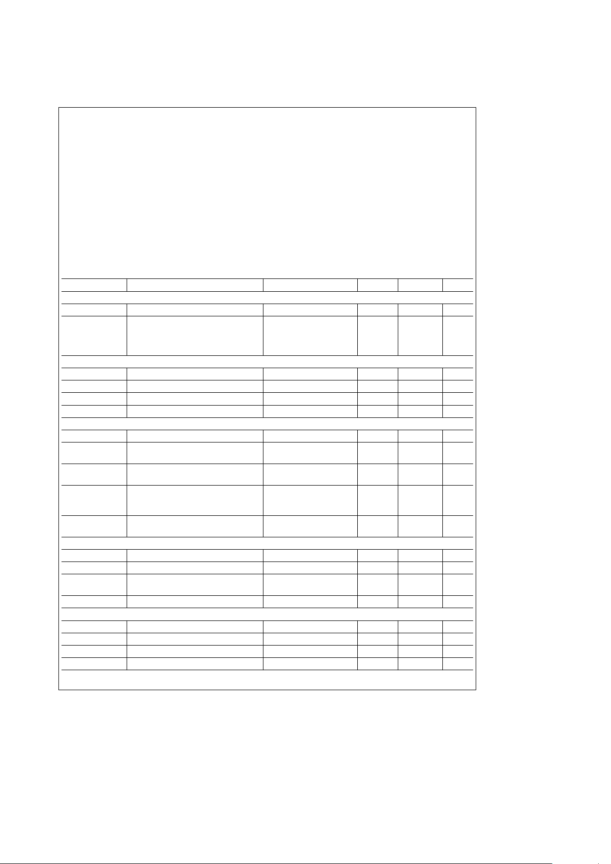
Block Diagram
TL/H/12317– 4
3
Page 4
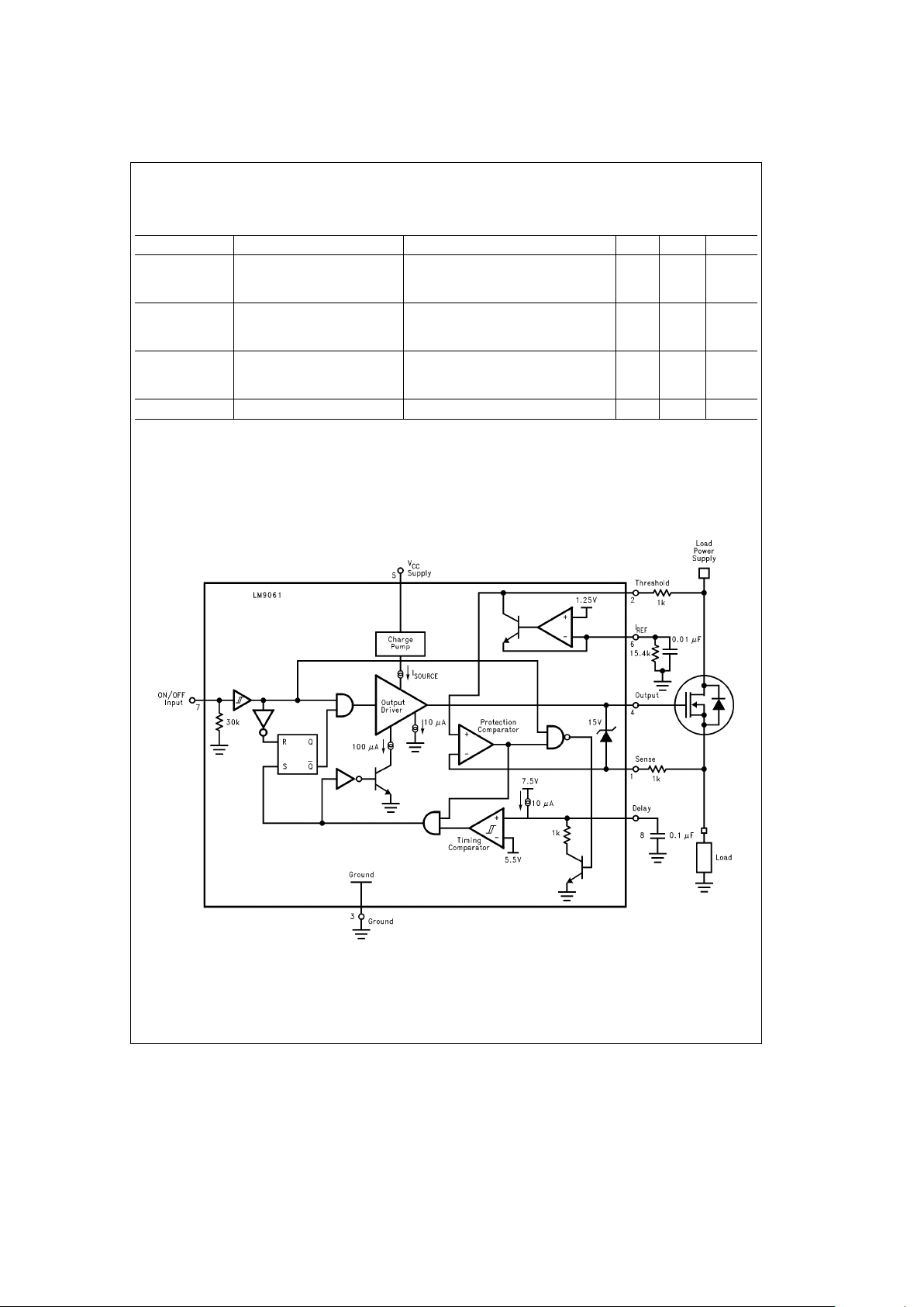
Typical Operating Waveforms
TL/H/12317– 5
4
Page 5
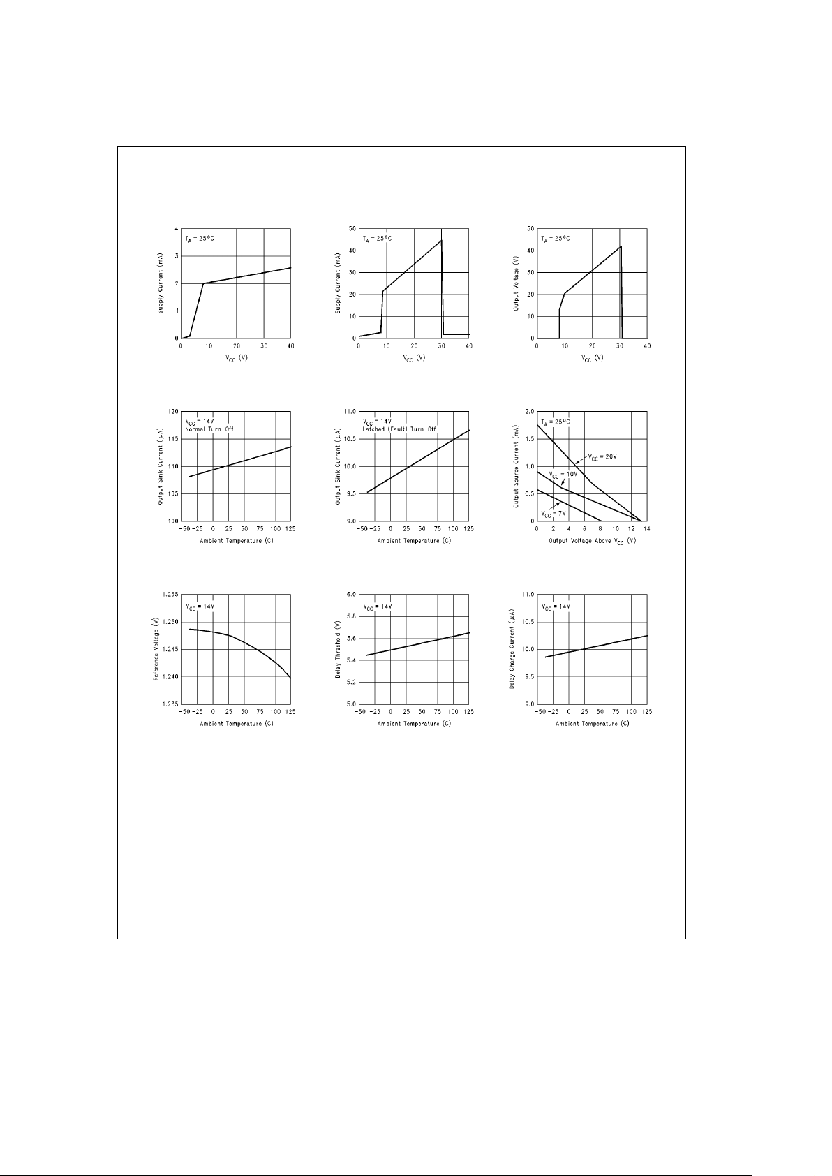
Typical Electrical Characteristics
vs V
CC
Standby Supply Current
vs V
CC
Operating Supply Current
vs V
CC
Output Voltage
vs Temperature
Output Sink Current
vs Temperature
Output Sink Current
vs Output Voltage
Output Source Current
vs Temperature
Reference Voltage
vs Temperature
Delay Threshold
vs Temperature
Delay Charge Current
TL/H/12317– 06
5
Page 6

Typical Electrical Characteristics (Continued)
Timing Definitions
TL/H/12317– 07
Application Hints
BASIC OPERATION
The LM9061 contains a charge pump circuit that generates
a voltage in excess of the applied supply voltage to provide
gate drive voltage to power MOSFET transistors. Any size
of N-channel power MOSFET, including multiple parallel
connected MOSFETs for very high current applications, can
be used to apply power to a ground referenced load circuit
in what is referred to as ‘‘high side drive’’ applications.
Figure 1
shows the basic application of the LM9061.
TL/H/12317– 8
FIGURE 1. Basic Application Circuit
When commanded ON by a logic ‘‘1’’ input to pin 7, the gate
drive output, pin 4, rises quickly to the V
CC
supply potential
at pin 5. Once the gate voltage exceeds the gate-source
threshold voltage of the MOSFET, V
GS(ON)
, (the source is
connected to ground through the load) the MOSFET turns
ON and connects the supply voltage to the load. With the
source at near the supply potential, the charge pump continues to provide a gate voltage greater than the supply to
keep the MOSFET turned ON. To protect the gate of the
MOSFET, the output voltage of the LM9061 is clamped to
limit the maximum V
GS
to 15V.
It is important to remember that during the Turn-ON of the
MOSFET the output current to the Gate is drawn from the
V
CC
supply pin. The VCCpin should be bypassed with a
capacitor with a value of at least ten times the Gate capacitance, and no less than 0.1 mF. The output current into the
Gate will typically be 30 mA with V
CC
at 14V and the Gate at
0V. As the Gate voltage rises to V
CC
, the output current will
decrease. When the Gate voltage reaches V
CC
, the output
current will typically be 1 mA with V
CC
at 14V.
A logic ‘‘0’’ on pin 7 turns the MOSFET OFF. When commanded OFF a 110 mA current sink is connected to the
output pin. This current discharges the gate capacitances of
the MOSFET linearly. When the gate voltage equals the
source voltage (which is near the supply voltage) plus the
V
GS(ON)
threshold of the MOSFET, the source voltage
starts following the gate voltage and ramps toward ground.
Eventually the source voltage equals 0V and the gate continues to ramp to zero thus turning OFF the power device.
This gradual Turn-OFF characteristic, instead of an abrupt
removal of the gate drive, can, in some applications, minimize the power dissipation in the MOSFET or reduce the
duration of negative transients, as is the case when driving
inductive loads. In the event of an overstress condition on
the power device, the turn OFF characteristic is even more
gradual as the output sinking current is only 10 mA (see
Protection Circuitry Section).
6
Page 7

Application Hints (Continued)
TURN ON AND TURN OFF CHARACTERISTICS
The actual rate of change of the voltage applied to the gate
of the power device is directly dependent on the input capacitances of the MOSFET used. These times are important
to know if the power to the load is to be applied repetitively
as is the case with pulse width modulation drive. Of concern
are the capacitances from gate to drain, C
GD
, and from gate
to source, C
GS
.
Figure 2
details the turn ON and turn OFF
intervals in a typical application. An inductive load is assumed to illustrate the output transient voltage to be expected. At time t1, the ON/OFF input goes high. The output,
which drives the gate of the MOSFET, immediately pulls the
gate voltage towards the V
CC
supply of the LM9061. The
source current from pin 4 is typically 30 mA which quickly
charges C
GD
and CGS. As soon as the gate reaches the
V
GS(ON)
threshold of the MOSFET, the switch turns ON and
the source voltage starts rising towards V
CC.VGS
remains
equal to the threshold voltage until the source reaches V
CC
.
While V
GS
is constant only CGDis charging. When the
source voltage reaches V
CC
, at time t2, the charge pump
takes over the drive of the gate to ensure that the MOSFET
remains ON.
The charge pump is basically a small internal capacitor that
acquires and transfers charge to the output pin. The clock
rate is set internally at typically 300 kHz. In effect the charge
pump acts as a switched capacitor resistor (approximately
67k) connected to a voltage that is clamped at 13V above
the Sense input pin of the LM9061 which is equal to the V
CC
supply in typical applications. The gate voltage rises above
V
CC
in an exponential fashion with a time constant depen-
dent upon the sum of C
GD
and CGS. At this time however
the load is fully energized. At time t3, the charge pump
reaches its maximum potential and the switch remains ON.
At time t4, the ON/OFF input goes low to turn OFF the
MOSFET and remove power from the load. At this time the
charge pump is disconnected and an internal 110 mA current sink begins to discharge the gate input capacitances to
ground. The discharge rate (DV/DT) is equal to 110 m A/
(C
GD
a
CGS).
The load is still fully energized until time t5 when the gate
voltage has reached a potential of the source voltage (V
CC
)
plus the V
GS(ON)
threshold voltage of the MOSFET. Be-
tween time t5 and t6, the V
GS
voltage remains constant and
the source voltage follows the gate voltage. With the voltage on C
GD
held constant the discharge rate now becomes
110 mA/C
GD
.
At time t6 the source voltage reaches 0V. As the gate
moves below the V
GS(ON)
threshold the MOSFET tries to
turn OFF. With an inductive load, if the current in the load
has not collapsed to zero by time t6, the action of the
MOSFET turning OFF will create a negative voltage transient (flyback) across the load. The negative transient will
be clamped to
b
V
GS(ON)
because the MOSFET must turn
itself back ON to continue conducting the load current until
the energy in the inductance has been dissipated (at time
t7).
MOSFET PROTECTION CIRCUITRY
A unique feature of the LM9061 is the ability to sense excessive power dissipation in the MOSFET and latch it OFF
to prevent permanent failure. Instead of sensing the actual
current flowing through the MOSFET to the load, which typically requires a small valued power resistor in series with
the load, the LM9061 monitors the voltage drop from drain
to source, V
DS
, across the MOSFET. This ‘‘lossless’’ technique allows all of the energy available from the supply to be
conducted to the load as required. The only power loss is
that of the MOSFET itself and proper selection of a particular power device for an application will minimize this concern. Another benefit of this technique is that all applications use only standard inexpensive (/4W or less resistors.
To utilize this lossless protection technique requires knowledge of key characteristics of the power MOSFET used. In
any application the emphasis for protection can be placed
on either the power MOSFET or on the amount of current
delivered to the load, with the assumption that the selected
MOSFET can safely handle the maximum load current.
TL/H/12317– 9
FIGURE 2. Turn ON and Turn OFF Waveforms
7
Page 8

Application Hints (Continued)
To protect the MOSFET from exceeding its maximum junction temperature rating, the power dissipation needs to be
limited. The maximum power dissipation allowed (derated
for temperature) and the maximum drain to source ON resistance, R
DS(ON)
, with both at the maximum operating ambient temperature, needs to be determined. When switched
ON the power dissipation in the MOSFET will be:
P
DISS
e
V
DS
2
R
DS(ON)
The VDSvoltage to limit the maximum power dissipation is
therefore:
V
DS (MAX)
e
0
P
D (MAX)
c
R
DS(ON) (MAX)
With this restriction the actual load current and power dissipation obtained will be a direct function of the actual
R
DS(ON)
of the MOSFET at any particular ambient temperature but the junction temperature of the power device will
never exceed its rated maximum.
To limit the maximum load current requires an estimate of
the minimum R
DS(ON)
of the MOSFET (the minimum
R
DS(ON)
of discrete MOSFETs is rarely specified) over the
required operating temperature range.
The maximum current to the load will be:
I
LOAD (MAX)
e
V
DS
R
DS(ON) (MIN)
The maximum junction temperature of the MOSFET and/or
the maximum current to the load can be limited by monitoring and setting a maximum operational value for the drain to
source voltage drop, V
DS
. In addition, in the event that the
load is inadvertently shorted to ground, the power device
will automatically be turned-OFF.
In all cases, should the MOSFET be switched OFF by the
built in protection comparator, the output sink current is
switched to only 10 mA to gradually turn OFF the power
device.
Figure 3
illustrates how the threshold voltage for the internal
protection comparator is established.
Two resistors connect the drain and source of the MOSFET
to the LM9061. The Sense input, pin 1, monitors the source
voltage while the Threshold input, pin 2, is connected to the
drain, which is also connected to the constant load power
supply. Both of these inputs are the two inputs to the protection comparator. Should the voltage at the sense input ever
drop below the voltage at the threshold input, the protection
comparator output goes high and initiates an automatic
latch-OFF function to protect the power device. Therefore
the switching threshold voltage of the comparator directly
controls the maximum V
DS
allowed across the MOSFET
while conducting load current.
The threshold voltage is set by the voltage drop across resistor R
THRESHOLD
. A reference current is fixed by a resis-
tor to ground at I
REF
, pin 6. To precisely regulate the reference current over temperature, a stable band gap reference
voltage is provided to bias a constant current sink. The reference current is set by:
I
REF
e
V
REF
R
REF
The reference current sink output is internally connected to
the threshold pin. I
REF
then flows from the load supply
through R
THRESHOLD
. The fixed voltage drop across
R
THRESHOLD
is approximately equal to the maximum value
of V
DS
across the MOSFET before the protection compara-
tor trips.
It is important to note that the programmed reference current serves a multiple purpose as it is used internally for
biasing and also has a direct effect on the internal charge
pump switching frequency. The design of the LM9061 is
optimized for a reference current of approximately 80 mA,
set with a 15.4 kX
g
1% resistor for R
REF
. To obtain the
guaranteed performance characteristics it is recommended
that a 15.4 kX resistor be used for R
REF
.
The protection comparator is configured such that during
normal operation, when the output of the comparator is low,
the differential input stage of the comparator is switched in
TL/H/12317– 11
FIGURE 3. Protection Comparator Biasing
8
Page 9

Application Hints (Continued)
a manner that there is virtually no current flowing into the
non-inverting input of the comparator. Therefore, only I
REF
flows through resistor R
THRESHOLD
. All of the input bias
current, 20 mA maximum, for the comparator input stage
(twice the I
SENSE
specification of 10 mA maximum, defined
for equal potentials on each of the comparator inputs) however flows into the inverting input through resistor R
SENSE
.
At the comparator threshold, the current through R
SENSE
will be no more than the I
SENSE
specification of 10 mA.
To tailor the V
DS (MAX)
threshold for any particular applica-
tion, the resistor R
THRESHOLD
can be selected per the fol-
lowing formula:
V
DS (MAX)
e
V
REF
c
R
THR
R
REF
b
(I
SENSE
c
R
SENSE
)aV
OS
where R
REF
e
15.4 kX,I
SENSE
is the input bias current to
the protection comparator, R
SENSE
is the resistor connect-
ed to pin 1 and V
OS
is the offset voltage of the protection
comparator (typically in the range of
g
10 mV).
The resistor R
SENSE
is optional, but is strongly recommended to provide transient protection for the Sense pin, especially when driving inductive type loads. A minimum value of
1kXwill protect the pin from transients ranging from
b
25V
to
a
60V. This resistor should be equal to, or less than, the
resistor used for R
THRESHOLD
. Never set R
SENSE
to a value
larger than R
THRESHOLD
. When the protection comparator
output goes high, the total bias current for the input stage
transfers from the Sense pin to the Threshold pin, thereby
changing the voltages present at the inputs to the comparator. For consistent switching of the comparator right at the
desired threshold point, the voltage drop that occurs at the
non-inverting input (Threshold) should equal, or exceed, the
rise in voltage at the inverting input (Sense).
In automotive applications the load supply may be the battery of the vehicle whereas the V
CC
supply for the LM9061
is a switched ignition supply. When the V
CC
supply is
switched OFF there is always a concern for the amount of
current drained from the battery. The only current drain under this condition is a leakage current into the Threshold pin
which is less than 10 mA.
A bypass capacitor across R
REF
is optional and is used to
help keep the reference voltage constant in applications
where the V
CC
supply is subject to high levels of transient
noise. This bypass capacitor should be no larger than
0.1 mF, and is not needed for most applications.
DELAY TIMER
To allow the MOSFET to conduct currents beyond the protection threshold for a brief period of time, a delay timer
function is provided. This timer delays the actual latching
OFF of the MOSFET for a programmable interval. This feature is important to drive loads which require a surge of
current in excess of the normal ON current upon start up, or
at any point in time, such as lamps and motors.
Figure 4
details the delay timer circuitry. A capacitor connected from
the Delay pin 8, to ground sets the delay time interval. With
the MOSFET turned ON and all conditions normal, the output of the protection comparator is low and this keeps the
discharge transistor ON. This transistor keeps the delay capacitor discharged. Should a surge of load current trip the
protection comparator high, the discharge transistor turns
OFF and an internal 10 mA current source begins linearly
charging the delay capacitor.
If the surge current, with excessive V
DS
voltage, lasts long
enough for the capacitor to charge to the timing comparator
threshold of typically 5.5V, the output of the comparator will
go high to set a flip-flop and immediately latch the MOSFET
OFF. It will not re-start until the ON/OFF Input is toggled
low then high.
The delay time interval is set by the selection of C
DELAY
and
can be found from:
T
DELAY
e
(V
TIMER
c
C
DELAY
)
I
DELAY
where typically V
TIMER
e
5.5V and I
DELAY
e
10mA.
Charging of the delay capacitor is clamped at approximately
7.5V which is the internal bias voltage for the 10 mA current
source.
MINIMUM DELAY TIME
A minimum delay time interval is required in all applications
due to the nature of the protection circuitry. At the instant
the MOSFET is commanded ON, the voltage across the
MOSFET, V
DS
, is equal to the full load supply voltage because the source is held at ground by the load. This condition will immediately trip the protection comparator. Without
a minimum delay time set, the timing comparator will trip
and force the MOSFET to latch OFF thereby never allowing
the load to be energized.
TL/H/12317– 12
FIGURE 4. Delay Timer
9
Page 10

Application Hints (Continued)
To prevent this situation a delay capacitor is required at pin
8. The selection of a minimum capacitor value to ensure
proper start-up depends primarily on the load characteristics
and how much time is required for the MOSFET to raise the
load voltage to the point where the Sense input is more
positive than the Threshold input (T
START-UP
). Some experimentation is required if a specific minimum delay time characteristic is desired. Therefore:
C
DELAY
e
(I
DELAY
c
T
START-UP
)
V
TIMER
In the absence of a specific delay time requirement, a value
for C
DELAY
of 0.1 mF is recommended.
OVER VOLTAGE PROTECTION
The LM9061 will remain operational with up to
a
26V on
V
CC
.IfVCCincreases to more than typicallya30V the
LM9061 will turn off the MOSFET to protect the load from
excessive voltage. When V
CC
has returned to the normal
operating range the device will return to normal operation
without requiring toggling the ON/OFF input. This feature
will allow MOSFET operation to continue in applications that
are subject to periodic voltage transients, such as automotive applications.
For circuits where the load is sensitive to high voltages, the
circuit shown in
Figure 5
can be used. The addition of a
zener on the Sense input (pin 1) will provide a maximum
voltage reference for the Protection Comparator. The Sense
resistor is required in this application to limit the zener current. When the device is ON, and the load supply attempts
to rise higher than (V
ZENER
a
V
THRESHOLD
), the Protection
comparator will trip, and the Delay Timer will start. If the high
supply voltage condition lasts long enough for the Delay
Timer to time out, the MOSFET will be latched off. The ON/
OFF input will need to be toggled to restart the MOSFET.
TL/H/12317– 13
FIGURE 5. Adding Over-Voltage Protection
REVERSE BATTERY
The LM9061 is not protected against reverse polarity supply
connections. If the V
CC
supply should be taken negative
with respect to ground, the current from the V
CC
pin should
be limited to 20 mA. The addition of a diode in series with
the V
CC
input is recommended. This diode drop does not
subtract significantly from the charge pump gate overdrive
output voltage.
LOW BATTERY
As an additional protection feature the LM9061 incorporates
an Undervoltage Shut-OFF function. If the V
CC
supply to the
package drops below 7V, where it may not be assured that
the MOSFET is actually ON when it should be, circuitry will
automatically turn OFF the power MOSFET.
Figure 6
shows the LM9061 used as an electronic circuit
breaker. This circuit provides low voltage shutdown, overvoltage latch OFF, and overcurrent latch OFF. In the event
of a latch OFF shutdown, the circuit can be reset by shutting
the main supply off, then back on. An optional reset switch
on the ON/OFF pin will allow a ‘‘push-button reset’’ of the
circuit after latching OFF.
TL/H/12317– 14
FIGURE 6. Electronic Circuit Breaker
Scaling of the external resistor value, from VCCto the ON/
OFF input pin, with the internal 30k resistor can be used to
increase the startup voltage. The circuit operation then becomes dependent on the resistor ratio and V
CC
providing an
ON/OFF pin voltage being above the ON threshold rather
than the LM9061 low V
CC
shutdown feature.
DRIVING MOSFET ARRAYS
The LM9061 is an ideal driver for any application that requires multiple parallel MOSFETs to provide the necessary
load current. Only a few ‘‘common sense’’ precautions need
to be observed. All MOSFETs in the array must have identical electrical and thermal characteristics. This can be
solved by using the same part number from the same
10
Page 11

Application Hints (Continued)
manufacturer for all of the MOSFETs in the array. Also, all
MOSFETs should have the same style heat sink or, ideally,
all mounted on the same heat sink. The electrical connection of the MOSFETs should get special attention. With typical R
DS(ON)
values in the range of tens of milli-Ohms, a
poor electrical connection for one of the MOSFETs can render it useless in the circuit.
Figure 7
shows a circuit with four parallel NDP706A
MOSFETs. This particular MOSFET has a typical R
DS(ON)
of 0.013X with a TJof 25§C, and 0.020X with a TJof
a
125§C.
With the V
DS
threshold voltage being set to 500 mV, this
circuit will provide a typical maximum load current of 150A
at 25
§
C, and a typical maximum load current of 100A at
125
§
C. The maximum dissipation, per MOSFET, will be
nearly 20W at 25
§
C, and 12.5W at 125§C. With up to 20W
being dissipated by each of the four devices, an effective
heat sink will be required to keep the T
J
as low as possible
when operating near the maximum load currents.
TL/H/12317– 15
FIGURE 7. Driving Multiple MOSFETs
11
Page 12

Application Hints (Continued)
TL/H/12317– 16
FIGURE 8. Increasing MOSFET Turn On Time
INCREASING MOSFET TURN ON TIME
The ability of the LM9061 to quickly turn on the MOSFET is
an important factor in the management of the MOSFET
power dissipation. Caution should be exercised when attempting to increase the MOSFET Turn On time by limiting
the Gate drive current. The MOSFET average dissipation,
and the LM9061 Delay time, must be recalculated with the
extended switching transition time.
Figure 8
shows a method of increasing the MOSFET Turn
On time, without affecting the Turn Off time. In this method
the Gate is charged at an exponential rate set by the added
external Gate resistor and the MOSFET Gate capacitances.
Although the LM9061 will drive MOSFETs from any manufacturer, National Semiconductor offers a wide range of
power MOSFETs.
Figure 9
shows a small sample of the
devices available.
Part I
D
V
DSSRDS(ON)
Package
NDP706A 75A 60V 0.015X TO-220
NDP706B 70A 60V 0.018X TO-220
NDP708A 60A 80V 0.022X TO-220
NDB708A 60A 80V 0.022X TO-263
NDP606A 48A 60V 0.025X TO-220
NDP606B 42A 60V 0.028X TO-220
NDP608A 36A 80V 0.042X TO-220
NDB608A 36A 80V 0.042X TO-263
NDP508A 19A 80V 0.080X TO-220
NDB508A 19A 80V 0.080X TO-263
NDP408A 11A 80V 0.160X TO-220
NDS9410 7A 30V 0.03X SO-8
NDS9936* 5A 30V 0.05X SO-8
NDS9945* 3.5A 60V 0.10X SO-8
* Dual
FIGURE 9. Recommended DMOS Power MOSFETs
12
Page 13

Physical Dimensions inches (millimeters)
Order Number LM9061M
NS Package Number M08A
13
Page 14

LM9061 Power MOSFET Driver with Lossless Protection
Physical Dimensions inches (millimeters) (Continued)
Order Number LM9061N
NS Package Number N08E
LIFE SUPPORT POLICY
NATIONAL’S PRODUCTS ARE NOT AUTHORIZED FOR USE AS CRITICAL COMPONENTS IN LIFE SUPPORT
DEVICES OR SYSTEMS WITHOUT THE EXPRESS WRITTEN APPROVAL OF THE PRESIDENT OF NATIONAL
SEMICONDUCTOR CORPORATION. As used herein:
1. Life support devices or systems are devices or 2. A critical component is any component of a life
systems which, (a) are intended for surgical implant support device or system whose failure to perform can
into the body, or (b) support or sustain life, and whose be reasonably expected to cause the failure of the life
failure to perform, when properly used in accordance support device or system, or to affect its safety or
with instructions for use provided in the labeling, can effectiveness.
be reasonably expected to result in a significant injury
to the user.
National Semiconductor National Semiconductor National Semiconductor National Semiconductor
Corporation Europe Hong Kong Ltd. Japan Ltd.
1111 West Bardin Road Fax: (
a
49) 0-180-530 85 86 13th Floor, Straight Block, Tel: 81-043-299-2309
Arlington, TX 76017 Email: cnjwge@tevm2.nsc.com Ocean Centre, 5 Canton Rd. Fax: 81-043-299-2408
Tel: 1(800) 272-9959 Deutsch Tel: (
a
49) 0-180-530 85 85 Tsimshatsui, Kowloon
Fax: 1(800) 737-7018 English Tel: (
a
49) 0-180-532 78 32 Hong Kong
Fran3ais Tel: (
a
49) 0-180-532 93 58 Tel: (852) 2737-1600
Italiano Tel: (
a
49) 0-180-534 16 80 Fax: (852) 2736-9960
National does not assume any responsibility for use of any circuitry described, no circuit patent licenses are implied and National reserves the right at any time without notice to change said circuitry and specifications.
 Loading...