

Page 1
TL/H/12372
LM9040 Dual Lambda Sensor Interface Amplifier
August 1995
LM9040
Dual Lambda Sensor Interface Amplifier
General Description
The LM9040 is a dual sensor interface circuit consisting of
two independent sampled input differential amplifiers designed for use with conventional Lambda Oxygen Sensors.
The Lambda Sensor is used for monitoring the oxygen concentration in the exhaust of gasoline engines using catalytic
after treatment and will deliver a voltage signal which is dependent on the air-fuel mixture. The gain of the amplifiers
are internally set and can directly convert the Lambda sensor output voltage to a level suitable for A/D conversion in a
system using a 5V reference.
The input common mode voltage range of each amplifier is
g
2V with respect to the IC ground pin. This will allow the IC
to connect to sensors which are remotely grounded at the
engine exhaust manifold or exhaust pipe.
Each amplifier is capable of independent default operation
should either, or both, of the leads to a sensor become
open circuited.
Noise filtering is provided by an internal switched capacitor
low pass filter as part of each amplifier, and by external
components.
The LM9040 is fully specified over the automotive temperature range of
b
40§Ctoa125§C and is provided in a 14-pin
Small Outline surface mount package.
Features
Y
Single 5V supply operation
Y
Common mode input voltage range ofg2V
Y
Differential input voltage range of 50 mV to 950 mV
Y
Sampled differential input
Y
Switched capacitor low pass filter
Y
Internal oscillator and VBBgenerator
Y
Open input default operation
Y
Cold sensor default operation
Y
Low power consumption (42 mW max)
Y
Gain set by design and guaranteed over the operating
temperature range
Applications
Y
Closed loop emissions control
Y
Catalytic converter monitoring
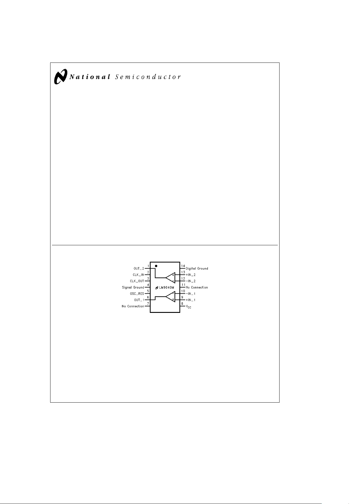
Connection Diagram
TL/H/12372– 1
Top View
Ordering Information
LM9040M
See NS Package Number M14B
C
1995 National Semiconductor Corporation RRD-B30M115/Printed in U. S. A.
Page 2
Absolute Maximum Ratings
If Military/Aerospace specified devices are required,
please contact the National Semiconductor Sales
Office/Distributors for availability and specifications.
Supply Voltage
b
0.3V toa6.0V
Input Voltage Continuous (Note 1)
g
14V
Input Voltage Transient t
s
1 ms (Note 1)
g
60V
ESD Susceptibility (Note 2)
g
2000V
Maximum Junction Temperature 150§C
Storage Temperature Range
b
65§Ctoa150§C
Lead Soldering Information
Vapor Phase (60 Seconds) 215
§
C
Infrared (15 Seconds) 220
§
C
Operating Ratings
Supply Voltage 4.75V to 5.25V
Differential Input Voltage 0V toa1V
Common Mode Voltage
g
2V
Power Dissipation 42 mW
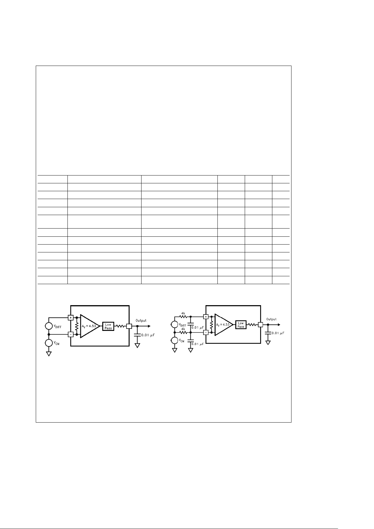
DC Electrical Characteristics
The following specifications apply for V
CC
e
5.0V, V
DIFF
e
500 mV, V
CM
e
0V, R
OSC
e
178 kX,b40§CsT
A
s
a
125§C, DC
Test Circuit
Figure 1
, unless otherwise specified.
Symbol Parameter Conditions Min Max Units
I
CC
Supply Current 4.75VsV
CC
s
5.25V 8.0 mA
Z
DIFF
Differential Input Impedance 4.75VsV
CC
s
5.25V 1.05 1.60 Meg X
Z
IO
Inverting Input to Ground Impedance Non-Inverting Inputs Open 10.00 Meg X
V
OL
Output Low Voltage V
DIFF
e
0V, I
LOAD
e
2.0 mA 100 mV
V
OC
V
OUT
Center One, or Both, Input(s) Open V
CC
#
0.380 V
CC
#
0.425 V
4.75V
s
V
CC
s
5.25V
V
OUT(ERROR)(VOUT
)–(V
DIFF
#
4.53) 50 mVsV
DIFF
s
950 mV, V
CM
e
0V
g
65 mV
V
OH
Output High Voltage V
DIFF
e
5V, I
LOAD
eb
2mAV
CC
b
0.1V V
R
OUT
Output Resistance 1500 3500 X
CMRR
(DC)
DC Common Mode Error
b
2VsV
CM
s
a
2V
g
4.5 mV/V
T
RISE
Output Rise Time C
OUT
e
0.01 mF 1.2 ms
T
FALL
Output Fall Time C
OUT
e
0.01 mF 1.2 ms
F
C
Low Pass Filterb3dB C
OUT
e
0.01 mF 400 700 Hz
Note 1: The input voltage must be applied through external 4 kX input resistors. See
Figure 2
, AC Test Circuit. Amplifier operation will be disrupted, but will not be
destructive.
Note 2: ESD rating is with Human Body Model: 100 pF discharged through a 1500X resistor.
TL/H/12372– 2
FIGURE 1. DC Test Circuit
TL/H/12372– 3
FIGURE 2. AC Test Circuit
2
Page 3
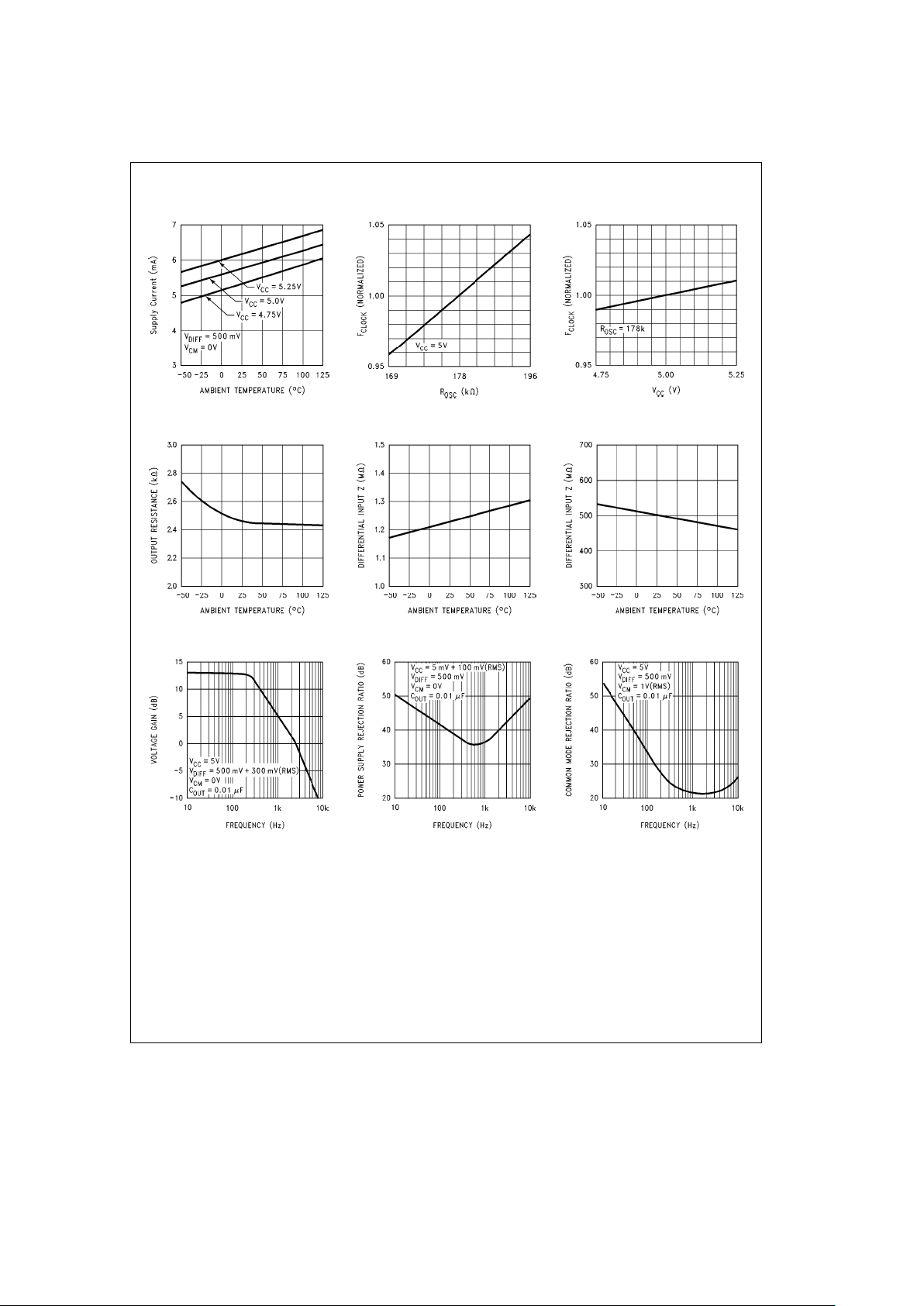
Typical Performance Characteristics
Supply Current vs Temperature
TL/H/12372– 4
F
CLOCK
(Normalized) vs R
OSC
TL/H/12372– 5
F
CLOCK
(Normalized) vs V
CC
TL/H/12372– 6
Output R vs Temperature
TL/H/12372– 7
Z
DIFF
vs Temperature
TL/H/12372– 8
FCvs Temperature
TL/H/12372– 9
Voltage Gain vs Frequency
TL/H/12372– 10
PSRR vs Frequency
TL/H/12372– 11
CMRR vs Frequency
TL/H/12372– 12
3
Page 4

Circuit Description
The LM9040 is fabricated in CMOS technology and is designed to operate from a single, well regulated, 5V supply.
The IC consists of two independent differential amplifiers
which are designed using two-phased switched capacitor
networks (SCN). The differential inputs have a common
mode operating range of 2V above and below ground. The
SCN includes the input sampling, the lowpass filter, cold
sensor bias voltage, and the gain circuitry. Each amplifier
has an independent voltage comparator to detect an open
inverting input pin. Additional support circuitry includes the
oscillator, clock generator, and V
BB
bias generator.
TL/H/12372– 13
FIGURE 3. Simplified Circuit
Oscillator
The device contains an internal oscillator which is used to
drive the internal two-phase clock generator. The oscillator
requires an external resistor value of 178 kX from the
‘‘OSCÐRES’’ pin to device V
CC
. This resistor value determines the charge rate of the internal capacitor, and thus
sets the oscillator frequency. The internal oscillator capacitor is matched to the switched capacitor networks, so that
the absolute capacitance values are not as important as is
the absolute ratios of the capacitors. The oscillator frequency is approximately 200 kHz.
The oscillator resistor should be located as close to the
OSCÐRES pin as possible. Any variation of the oscillator
resistor value, any stray capacitance on the OSCÐRES pin,
or any changes in the supply voltage, will result in a change
in the oscillator frequency. This will directly affect the device
Differential Input Impedance, and Low Pass filter response.
Additional circuitry takes the oscillator signal and generates
two non-overlapping clock signals, and a CLKÐOUT signal.
The clock signals operate at one half the oscillator frequency, or typically 100 kHz. This results in a Nyquist frequency
of typically 50 kHz.
Clock Out/Clock In
For the input stage to work with common mode voltages
below Ground potential, a negative bias voltage (V
BB
)is
needed. The CLKÐOUT pin is used to provide the AC signal needed to drive the internal V
BB
bias generator through
an external coupling capacitor. A minimum coupling capacitor value of 100 pF to a maximum value of 0.1 mF is recommended. The CLKÐIN pin is the input to the V
BB
bias gen-
erator circuitry.
Differential Input Circuit
The input stage can be best described as a switched Sample and Difference circuit (see
Figure 4
). When the input
capacitor C
IN
is switched to the non-inverting input, the in-
put voltage plus the common mode voltage is stored on C
IN
.
When C
IN
is switched to the inverting input, CINwill be discharged by an amount equal to the common mode voltage.
The remaining charge across C
IN
will be equal to the differential input voltage, and a proportional charge will be transferred through the virtual ground via the gain stage.
TL/H/12372– 14
FIGURE 4. Simplified Switched Capacitor Input Circuit
4
Page 5

Differential Input Circuit (Continued)
The differential input impedance is a function of the value of
the input capacitor array and the sampling frequency. The
capacitor C
BIAS
is used to generate a bias voltage across
the Differential Input impedance (Z
DIFF
). This bias voltage is
similar to the Lambda Sensor output voltage at the stoichiometric air-fuel mixture (l
e
1). The bias voltage is set by the
ratio of C
IN
and C
BIAS
, and the value of VCC.
The resulting bias voltage across the Differential Input is
defined as:
V
BIAS
e
V
CC
#
C
BIAS
(C
IN
a
C
BIAS
)
With C
BIAS
e
0.7286 pF, C
IN
e
7.421 pF, F
CLOCK
e
100 kHz, and V
CC
e
5V:
V
BIAS
e
5#7.286E-13
(7.4213E-12a7.286E-13)
V
BIAS
e
447 mV
In effect, the result is the same as forcing a bias current
through the Differential Input impedance.
The bias current is defined as:
I
BIAS
e
V
CC
#
C
BIAS
#
F
CLOCK
I
BIAS
e
364.3 nA
The Differential Input impedance is defined as:
Z
DIFF
e
1
(C
IN
a
C
BIAS
)#F
CLOCK
Z
DIFF
e
1.227 MX
This bias voltage will be developed across the Differential
Input impedance (Z
DIFF
) if there is no other path available
from the non-inverting input pin for I
BIAS
, and the inverting
input has a current path to ground. See
Figure 5
. During
normal operating conditions I
BIAS
will have a negligible ef-
fect on accuracy
TL/H/12372– 15
FIGURE 5. Equivalent Input Bias Circuit
Differential Input Filtering
Since each input is sampled independently, an anti-aliasing
filter is required at the amplifier inputs to ensure that the
input signal does not exceed the Nyquist frequency.
This external low-pass filter is implemented by adding a capacitor (C
DIFF
) across the differential input. See
Figure 6
.
This forms an RC network across the differential inputs in
conjunction with the required external 4 kX resistors and
the differential input impedance (Z
DIFF
). The capacitor selected should be small enough to have minimal effect on
gain accuracy in the application, yet large enough to filter
out unwanted noise. Given that the F
C
of the LM9040 is
typically 500 Hz, the use of a 0.01 mF capacitor will generally provide adequate filtering, with less than
b
0.4 dB of input
attenuation at 500 Hz and approximately
b
28 dB at 50 kHz.
A larger value capacitor can be used if needed, but a value
larger than typically 0.02 mF will begin to dominate the cutoff frequency of the application. This capacitor must be a
low leakage and low ESR type so that circuit performance is
not degraded.
TL/H/12372– 16
FIGURE 6. Differential and Common Mode Filtering
Common Mode Filtering
The differential input sampling of the LM9040 actually reduces the effects of common mode input noise at low frequencies. The time interval between the sampling of the
inverting input and the non-inverting input is one half of a
clock period. A change in the common mode voltage during
this short time interval can cause an error in the charge
stored on C
IN
. This will result in an error seen on the output
voltage. For a sine-wave common mode voltage the minimum common mode rejection is:
CMRR
e
2
#q#
F
CMR
#
(0.5/F
CLOCK
)#4.53
Where F
CMR
is the frequency of the common mode signal,
and F
CLOCK
is the clock frequency.
5
Page 6

Common Mode Filtering (Continued)
For a common mode sine wave signal having a frequency
100 Hz, and with a F
CLOCK
of 100 kHz, the minimum com-
mon mode rejection would be:
CMRR
e
2#3.14159#100#5E-6#4.53
CMRRe0.014eb37 dB
If the common mode sine wave has a peak to peak value of
2V, the maximum voltage error at the output would be:
V
OUT(CM)
e
2V#0.014e28 mV
As this formula shows, the value of V
OUT(CM)
is proportional
to the frequency of the CMR signal. If the frequency is doubled, the value of V
OUT(CM)
is also doubled. The addition of
a small bypass capacitor (C
CM
) from the non-inverting input
to ground will help counter this problem. See
Figure 6
. However, the use of this bypass capacitor creates a new problem in that the differential input is no longer balanced. While
the Lambda sensor is cold (i.e. R
SENSOR
l
10 MegX) there
is little difference in CMR performance. As the Lambda sensor heats to the operating temperature and the sensor resistance decreases, the common mode signal is no longer
applied to both inputs equally. This imbalance causes
V
OUT(CM)
to increase as R
SENSOR
decreases, as the noninverting input will see the full common mode signal, while
the non-inverting input will see an attenuated common
mode signal.
The selection of the value of the CMR bypass capacitor
needs to be balanced with the need for reasonable reduction, or elimination, of common mode signals with both cold
and hot sensors. Since normal operation will need to include consideration of the entire impedance range of the
sensor, a trade off in overall application performance may
be needed.
Generally, the value of the CMR bypass capacitor should be
kept as low as possible, and should not be larger than the
differential input filter capacitor. Values in the range of
0.001 mF to 0.01 mF will usually provide reasonable CMR
results, but optimum results will need to be determined empirically, as the source of common mode signals will be
unique to each application.
Gain and Filter Stage
The signal gain and filter stage is designed to have a DC
gain of 4.53 V/V, with a cut-off frequency of typically
500 Hz. The external 4 kX resistors on each input pin are in
series with the differential input impedance. Together they
form a voltage divider circuit across the input such that the
net DC gain of the application circuit is 4.50 V/V.
TL/H/12372– 17
FIGURE 7. Simplified Gain and Filter Circuit
The internal gain is set by the ratio of C
IN
and CFB:
GAIN
DC
e
C
IN
C
FB
GAIN
DC
e
7.4213 pF
1.6383 pF
e
4.53 V/V
The corner frequency (
b
3 dB) is set by the ratio of CFBand
C
INT
, and by F
CLOCK
:
F
C
e
F
CLOCK
#
C
FB
2
#q#
C
INT
F
C
e
1E5#1.6383E-12
2#3.14159#52.1E-12
e
500 Hz
TL/H/12372– 18
FIGURE 8. Equivalent Gain and Filter Circuit
6
Page 7

Cold Sensor
Typically, a Lambda sensor will have an impedance of less
than 10 kX when operating at temperatures between 300
§
C,
and 500
§
C. When a Lambda sensor is not at operating temperature, its impedance can be more than 10 MegX. Any
voltage signal that may be developed is seriously attenuated. During this high impedance condition the LM9040 will
provide a default output voltage.
TL/H/12372– 19
FIGURE 9. V
OUT
with Cold Lambda Sensor
Each amplifier input has a bias charge applied across the
Differential Input impedance (Z
DIFF
) by means of charge
redistribution through the switched capacitor network. This
bias charge is a ratio of V
CC
, and is typically 447 mV for a
V
CC
value of 5.00V. This will provide an output voltage of
typically 2.025V.
While the Lambda sensor is high impedance, the 447 mV
across Z
DIFF
will be the dominant input signal. As the Lambda sensor is heated, and the sensor impedance begins to
drop, the voltage signal from the sensor will become the
dominate signal.
Output Resistance
With normal operation, each output has typically 2.5 kX of
resistance. This resistance, along with an external capacitor, form a RC low pass filter to remove any clock noise
from the output signal. An external output filter capacitor
value of 0.01 mF is recommended. Additionally, the output
resistance will provide current limiting for the output stage
should it become shorted to Ground or V
CC
.
Any DC loading of the output will cause an error in the measured output voltage. This error will be equal to the I
#
R drop
across the output resistance:
V
ERROR
e
I
LOAD
#
2.5 kX
Open Input Pins Defaults
In any remote sensor application it is desirable to be able to
deal with the possibility of open connections between the
sensor and the control module. The LM9040 is capable of
providing an output voltage scaled to V
CC
should either, or
both, of the wires to the Lambda sensor open. The two
inputs handle the open circuit condition differently. The
LM9040 will provide a default V
OUT
that is typically 2.025V
when V
CC
is at 5V.
For the case of an open connection of the non-inverting
input, the device would react the same as for the Cold Sensor condition. The internal bias voltage across Z
IN
would
cause the output voltage to be at a value defined by V
CC
and the LM9040 DC gain. The inverting input would still be
connected to the Lambda sensor ground, so any common
mode signals would still need to be allowed for in this condition. See
Figure 9
.
For the case of an open connection of the inverting input,
the device output stage switches from the amplifier output
to a resistive voltage divider. In this case, the default V
OUT
is not dependent on the gain stage, and any signal on the
non-inverting input will have no effect on the output. Each
amplifier has a comparator to monitor the voltage on the
inverting input pin. When the voltage on an inverting pin
goes above typically 2.5V, the comparator will switch the
output from the amplifier output to the voltage divider stage.
To fully implement this function requires external pull-up resistors for each of the inverting inputs. To minimize signal
errors due to DC currents through the 4 kX resistors, the
pull-up resistors need to be added in the application circuit
between the 4 kX input resistor and the connection to the
Lambda sensor ground point. A typical pull-up value of
51 kX to V
CC
is recommended. During this condition, the
effective resistance of the output stage will be 3.5 kX typically. See
Figure 10
.
TL/H/12372– 20
FIGURE 10. V
OUT
with Open Inverting Input
7
Page 8

Open Input Pins Defaults (Continued)
In the cases where both the inverting and non-inverting pins
are open, the non-inverting condition (i.e.: voltage divider
across the output) will be the dominant condition.
Any common mode signal seen by inverting input pin should
not be allowed to exceed the Common Mode voltage range.
Exceeding the positive Common Mode voltage limit could
cause the inverting input pin voltage comparator to act as if
the inverting input pin is open. Since the comparator circuit
is not part of the switched capacitor network there is no
frequency limitation on the signal to the comparator. Any
transient on the inverting input pin which goes above the
comparator threshold will immediately cause the output to
switch to the open sensor mode. The output will return to
normal operation when the voltage on the inverting input
falls below the comparator threshold.
Supply Bypassing
For best performance the LM9040 requires a VCCsupply
which is stable and noise free. The same 5V V
REF
supply
used for the A/D converter is the recommended V
CC
supply. During operation the device will generate current spikes
coincident with the clock edges. Inadequate bypassing will
cause excessive clock noise on the outputs, as well as
noise on the V
CC
line. The LM9040 VCCpin should be bypassed with a minimum 0.1 mF capacitor to the Signal
Ground pin, and should be located as close to the device as
possible. Some applications may require an additional
4.7 mF tantalum capacitor, especially if there are several
other switched capacitor devices running off the same 5V
supply line. The Signal and Digital Ground pins should be
tied together as close to the device as possible.
TL/H/12372– 21
FIGURE 11. Typical Application
8
Page 9

9
Page 10

LM9040 Dual Lambda Sensor Interface Amplifier
Physical Dimensions inches (millimeters)
14-Lead (0.300×Wide) Molded Small Outline Package, JEDEC
Order Number LM9040M
NS Package Number M14B
LIFE SUPPORT POLICY
NATIONAL’S PRODUCTS ARE NOT AUTHORIZED FOR USE AS CRITICAL COMPONENTS IN LIFE SUPPORT
DEVICES OR SYSTEMS WITHOUT THE EXPRESS WRITTEN APPROVAL OF THE PRESIDENT OF NATIONAL
SEMICONDUCTOR CORPORATION. As used herein:
1. Life support devices or systems are devices or 2. A critical component is any component of a life
systems which, (a) are intended for surgical implant support device or system whose failure to perform can
into the body, or (b) support or sustain life, and whose be reasonably expected to cause the failure of the life
failure to perform, when properly used in accordance support device or system, or to affect its safety or
with instructions for use provided in the labeling, can effectiveness.
be reasonably expected to result in a significant injury
to the user.
National Semiconductor National Semiconductor National Semiconductor National Semiconductor
Corporation Europe Hong Kong Ltd. Japan Ltd.
1111 West Bardin Road Fax: (
a
49) 0-180-530 85 86 13th Floor, Straight Block, Tel: 81-043-299-2309
Arlington, TX 76017 Email: cnjwge@tevm2.nsc.com Ocean Centre, 5 Canton Rd. Fax: 81-043-299-2408
Tel: 1(800) 272-9959 Deutsch Tel: (
a
49) 0-180-530 85 85 Tsimshatsui, Kowloon
Fax: 1(800) 737-7018 English Tel: (
a
49) 0-180-532 78 32 Hong Kong
Fran3ais Tel: (
a
49) 0-180-532 93 58 Tel: (852) 2737-1600
Italiano Tel: (
a
49) 0-180-534 16 80 Fax: (852) 2736-9960
National does not assume any responsibility for use of any circuitry described, no circuit patent licenses are implied and National reserves the right at any time without notice to change said circuitry and specifications.
 Loading...