

Page 1
LM9011
Electronic Ignition Interface
General Description
The LM9011 is an interface circuit which integrates the timing detection and logic control functions required for an automotive electronic ignition system into one device.
A VRS interface is provided for crankshaft position information via a toothed-wheel.
Four voltage comparators are provided for hardware diagnostics.
An electronic timing interface with output fault diagnostics is
provided to enable a micro-processor to drive an external
four channel ignition spark circuit.
The LM9011 is fully specified over the automotive temperature range of -40˚C to +125˚C, and is available in a 28 pin
Small Outline surface mount package.
Key Specifications
Features
n Single 5V supply operation
n VR Sensor Interface with dynamic hysteresis
n Four Channel Electronic Timing spark driver with output
diagnostics
n Electronic Timing Interface spark driver output voltage
from 5V to 16V
n One Non-Inverting voltage comparator with hysteresis
n Three Inverting voltage comparators with hysteresis
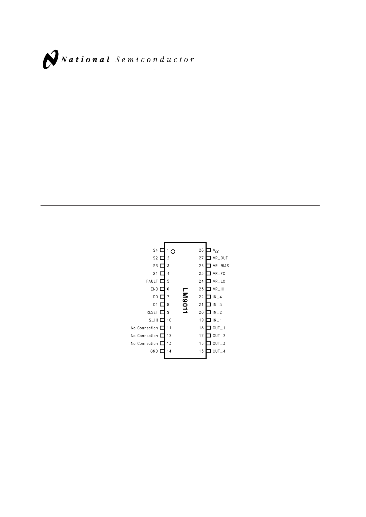
Connection Diagram
Top View
DS101264-1
Ordering Information LM9011M
See NS Package M28B
February 2000
LM9011 Electronic Ignition Interface
© 2000 National Semiconductor Corporation DS101264 www.national.com
Page 2
Absolute Maximum Ratings (Note 1)
Voltage -0.3V to +7.0V
S_HI Voltage -0.3V to 26.5V
VR_HI and VR_LO Inputs +/-3mA
Comparator Inputs -0.3V to +7.0V
Timing Interface Inputs -0.3V to +7.0V
ESD Susceptibility (Note 3) +/-2000V
Maximum Junction Temperature 150˚C
Storage Temperature Range -65˚C to +150˚C
Lead Soldering Information:
Vapor Phase (60 Seconds) 215˚C
Infrared (15 Seconds) 220˚C
Operating Ratings (Note 3)
V
CC
Voltage 4.75V to 5.25V
S_HI Voltage V
CC
to 26V
Sx Outputs -0.3V to S_HI +0.3V
Comparator Inputs
VR_HI and VR_LO Inputs
-0.3V to V
CC
+0.3V
+/-2.75mA
Timing Interface Inputs -0.3V to V
CC
+0.3V
Thermal Resistances (M28B):
Junction to Case (θJ-C) 15˚C/W
Junction to Ambient (θJ-C) 69˚C/W
DC Electrical Characteristics The following specifications apply for V
CC
= 5V, V
RESET=VCC,VS_HI
=
V
CC
, -40˚C ≤ TA≤ +125˚C, Application Circuit Figure 16, unless otherwise specified.
Symbol Parameter Conditions Minimum Maximum Units
I
CC
Supply Current
RESET, IN_4 = V
CC
25 mA
ENB, D0, D1, IN_1, IN_2, IN_3 =
0V
VR_HI = +12.5µA
VR_LO = -12.5µA
Comparators
V
TH
1 Input Threshold VIN_1 Decreasing from VCCto 0V
until V
OUT
_1>VCC/2
V
CC
X 0.435 VCCX 0.485 V
V
TH
2 Input Threshold VIN_2 Decreasing from VCCto 0V
until V
OUT
_2>VCC/2
V
CC
X 0.435 VCCX 0.485 V
V
TH
3 Input Threshold VIN_3 Decreasing from VCCto 0V
until V
OUT
_3>VCC/2
V
CC
X 0.40 VCCX 0.45 V
V
TH
4 Input Threshold VIN_4 Decreasing from VCCto 0V
until V
OUT
_4<VCC/2
V
CC
X 0.45 VCCX 0.50 V
V
HYST
Input Hysteresis All Comparators 150 400 mV
I
BIAS
Input Bias Current IN_1, IN_2, IN_3 = 0V ≤ VIN≤V
CC
IN_4 = 0V ≤ VIN_4 ≤ VCC-1V
750 µA
V
OH
Output High Voltage I
LOAD
= -100µAV VCC-1 V
V
OL
Output Low Voltage I
LOAD
= +100µAV 750 mV
VR Sensor Interface
V
OH
Output High Voltage I
LOAD
= -15µA
VR_HI= -1mA, VR_LO = +1mA
VCC-1 V
V
OL
Output Low Voltage Load = +15µA
VR_HI=+1mA, VR_LO = -1mA
750 mV
I
DIFF(MIN)
Minimum Detect Differential Input
Current (Note 4)
-40˚C ≤ TA≤ +25˚C
T
A
= +85˚C (Note 7)
T
A
= +125˚C
0.5
0.6
1.0
3.0
3.5
5.0
uA Pk-Pk
uA Pk-Pk
uA Pk-Pk
I
HYS
1 Input Hysteresis (Note 4) I
DIFF
= 1mA pk-pk 75 250 uA Pk
I
HYS
2 Input Hysteresis (Note 4) I
DIFF
= 2.5mA pk-pk 185 625 uA Pk
Electronic Timing Interface
V
IH
Input Logic 1 D0, D1, ENB,
RESET
VCCX 0.7 V
V
IL
Input Logic 0 D0, D1, ENB,
RESET
VCCX 0.3 V
I
IH
Input High Current Inputs D0, D1,
RESET
VIN=V
CC
10 µA
I
IH
Input High Current Input ENB VIN=V
CC
125 µA
LM9011
www.national.com 2
Page 3
DC Electrical Characteristics The following specifications apply for V
CC
= 5V, V
RESET
=VCC,V
S_HI=VCC
,
-40˚C ≤ T
A
≤ +125˚C, Application Circuit Figure 16, unless otherwise specified. (Continued)
Symbol Parameter Conditions Minimum Maximum Units
Electronic Timing Interface
I
IL
Input Low Current Inputs D0, D1,
ENB
VIN= 0V -10 µA
I
IL
Input Low Current Input RESET VIN= 0V -125 µA
V
OH
Output High Voltage Outputs S1,
S2, S3, S4
I
LOAD
= -10mA, V
S_HI
= 5V 3.75 V
V
OL
Output Low Voltage Outputs S1,
S2, S3, S4
I
LOAD
= 1mA, V
S_ HI
= 5V 300 mV
V
OH
Output High Voltage Outputs S1,
S2, S3, S4
I
LOAD
= -10mA, V
S_HI
= 16V 14 V
V
OL
Output Low Voltage Outputs S1,
S2, S3, S4
I
LOAD
= 1mA, V
S_HI
=16V 450 mV
V
OH
Output High Voltage Outputs S1,
S2, S3, S4
I
LOAD
= -10mA, V
S_HI
=26V 22 V
V
OL
Output Low Voltage Outputs S1,
S2, S3, S4
I
LOAD
= 1mA, V
S_HI
=26V 600 mV
V
OH
FAULT Pin Output High Voltage I
FAULT
= -100µA, no fault VCC-1 V
V
OL
FAULT Pin Output Low Voltage I
FAULT
= 100µA, any fault 750 mV
V
FAULT
Fault Treshold Voltage Outputs
S1, S2, S3, S4
Sx Output Short Fault VCCX 0.2 VCCX 0.5 V
I
FOL
TRI-STATE Output Current
Outputs S1, S2, S3, S4
V
RESET
= 0V, V
S _HI
=5V
R
LOAD
= 10KΩ
-12 -50 µA
AC Electrical Characteristics
The following specifications apply for VCC= 5V, V
S_HI=VCC,VRESET=VCC
, -40˚C≤TA≤+125˚C. The AC Timing Characteristics
are not production tested. Minimum and Maximum limits are guaranteed by device characterization.
Symbol Parameter Conditions Minimum Maximum Units
Comparators
T
RISE
Output Rise Time 10%to 90%,C
LOAD
= 25pF 5 µs
T
FALL
Output Fall Time 90%to10%,C
LOAD
= 25pF 5 µs
VR Sensor Interface (Note 4)
T
RISE
Output Rise Time 10%to 90%,C
LOAD
= 100pF,
R
LOAD
= 100KΩ
10 µs
T
FALL
Output Fall Time 90%to10%,C
LOAD
= 100pF,
R
LOAD
= 100kΩ
5ms
T
DELAY
Zero Crossing Delay Time (Note6)I
DIFF
= 5µA pk-pk, F
VRS
= 200Hz
I
DIFF
= 50µA pk-pk, F
VRS
=
2.5KHz
1
10
ms
ms
F
MAX
Maximum VRS Frequency C
LOAD
= 100pF, R
LOAD
= 100KΩ
I
DIFF
= 5µA pk-pk
50 KHz
Electronic Timing Interface
T
RISE
1 Sx Output Rise Time Sx Rises10%to 90
%
C
LOAD
= 6.8nF, R
LOAD
= 10KΩ 5µs
C
LOAD
= 12.7nF, R
LOAD
= 10KΩ 8µs
T
FALL
1 Sx Output Fall Time Sx Falls 90%to 10
%
C
LOAD
= 6.8nF, R
LOAD
= 10KΩ 15 µs
C
LOAD
= 12.7nF, R
LOAD
= 10KΩ 25 µs
T
SETUP
SetupTime (Notes 7, 8 and 9) 1 µs
T
HOLD
Hold Time 0.5 µs
LM9011
www.national.com3
Page 4
AC Electrical Characteristics (Continued)
The following specifications apply for VCC= 5V, V
S_HI=VCC,VRESET=VCC
, -40˚C≤TA≤+125˚C. The AC Timing Characteristics
are not production tested. Minimum and Maximum limits are guaranteed by device characterization.
Symbol Parameter Conditions Minimum Maximum Units
Electronic Timing Interface
T
DF
1 Fault Delay Time Sx Output Short to Ground Fault
From ENB=1toFAULT ≤ 10
%
C
FAULT
= 25pF 2 µs
T
DF
2 Fault Delay Time Sx Output Short to Battery Fault
From ENB=0toFAULT ≤ 10
%
C
FAULT
= 25pF 2 µs
T
TRI
TRI-STATE Delay Time From RESET=0toAllSx
Outputs Off
2µs
T
RISE
2 Fault Pin Rise Time 10%to 90%,C
FAULT
= 25pF 5 µs
T
FF(OFF)
False Fault Time From ENB=0toFAULT ≥ 90
%
C
FAULT
= 25pF
C
LOAD
= 6.8nF, R
LOAD
= 10KΩ 25 µs
C
LOAD
= 12.7nF, R
LOAD
= 10KΩ 30 µs
T
FF(ON)
False Fault Time From ENB=1toFAULT ≥ 90
%
C
FAULT
= 25pF
C
LOAD
= 6.8nF, R
LOAD
= 10KΩ 8µs
C
LOAD
= 12.7, R
LOAD
= 10KΩ 10 µs
T
UDF
Undefined Fault Time From ENB = 0 for 8uSec, to Valid
FAULT
C
LOAD
= 6.8nF, R
LOAD
= 10KΩ 20 µs
C
LOAD
= 12.7nF, R
LOAD
= 10KΩ 25 µs
Note 1: Absolute Maximum Ratings indicate the limits beyond which damage may occur.
Note 2: ESD Ratings is with Human Body Model: 100pF discharged through a 1500Ω resistor.
Note 3: Operating ratings indicateconditions for which the device is intended to be functional, but may not meet the guaranteed specificperformance limits. For guar-
anteed specifications and conditions, see the Electrical Characteristics.
Note 4: Tested per VR Sensor Interface test circuit. See figures 8 and 9.
Note 5: Minimum Detect Current is not production tested at +85C. Specifications is guaranteed through device characterization and Test Limits at 25˚C and 125˚C.
Note 6: VR Sensor Interface Tdelay, measured from VR input sine wave zero-crossing to VR_OUT going high. See figure 9.
Note 7: Electronic Timing Interface Tsetup, minimum time between Vcc
>
4.75V and RESET = 1.
Note 8: Electronic Timing Interface Tsetup, minimum time between RESET = 1 and D0 = 1.
Note 9: Electronic Timing Interface Tsetup, minimum time between D0 / D1 = valid and ENB = 1.
LM9011
www.national.com 4
Page 5
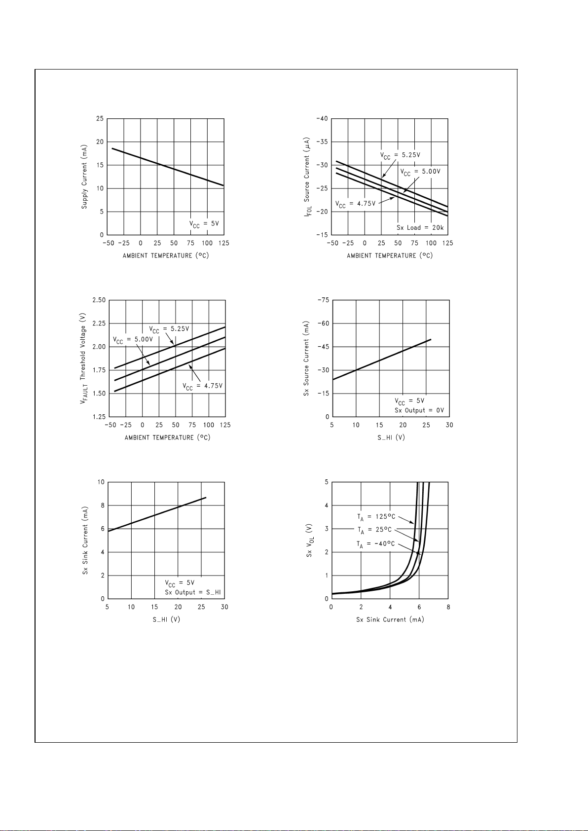
Typical Performance Characteristics
Supply Current vs Temperature
DS101264-3
Ifol Source Current vs Temperature
DS101264-4
VFault Threshold vs Temperature
DS101264-5
Sx Source Current vs S_HI Voltage
DS101264-6
Sx Sink Current vs S_HI Voltage
DS101264-7
Sx Vol vs Sx Sink Current
DS101264-8
LM9011
www.national.com5
Page 6

Typical Performance Characteristics (Continued)
Sx Voh vs Sx Source Current
DS101264-9
VRS Interface Minimum Detect
vs Temperature
DS101264-10
VRS Interface Minimum Detect
vs VR_BIAS
DS101264-11
LM9011
www.national.com 6
Page 7

Timing Diagrams
DS101264-12
FIGURE 1. Electronic Timing Interface Timing Diagram
DS101264-13
FIGURE 2. Fault Pin Timing During Sx Shorted to Ground
DS101264-14
FIGURE 3. Fault Pin Timing During Sx Shorted to Battery
LM9011
www.national.com7
Page 8

Timing Diagrams (Continued)
DS101264-15
FIGURE 4. False FAULT Time for Disabled Sx Output
DS101264-16
FIGURE 5. False FAULT Time for Enabled Sx Output
LM9011
www.national.com 8
Page 9

Timing Diagrams (Continued)
DS101264-17
FIGURE 6. Time for Valid Fault Detection
DS101264-18
FIGURE 7. Electronic Timing Interface Typical Waveforms
LM9011
www.national.com9
Page 10

Timing Diagrams (Continued)
DS101264-19
FIGURE 8. VR Interface Test Circuit
DS101264-20
FIGURE 9. VR Interface Timing Diagram
LM9011
www.national.com 10
Page 11

Circuit Description
VR Sensor Interface
The differential inputs, VR_HI and VR_LO are low impedance inputs with a DC voltage bias of one half of Vcc, Both
inputs require equal value series resistance on their respective pins to convert the VR sensor voltage to a differential input current. The differential input current range is typically
2.5µA peak-to-peak to 2.5mA peak-to-peak. Each input has
active current limiting that will clamp the current at typically
+/-5mA. This is intended for short circuit protection and not
for input signal limiting.
Differential voltages of 500mV peak-to-peak to 500V peakto-peak can be processed with the specified 100KΩ series
resistor on each input. Numerous variables will determine
the output voltage signal from a VR sensor across a frequency range. The input resistors can be scaled from typically 50KΩ to 200KΩ to keep the differential input current
with-in the recommended range for a given VR Sensor output voltage. Bypass capacitors can be added to form a low
pass filter to limit the differential inputsignalatthehigher frequencies.
The VR Sensor interface utilizes a dynamic hysteresis which
will increase the hysteresis level as the input signal from the
VR Sensor increases. The circuit requires two external components to fully implement the hysteresis function: a capacitor on VR_FC to filter and store the peak detector signals;
and a 150KΩ resistor on VR_BIAS to set a reference current
for the hysteresis circuit.Thetypical value range for the peak
detector storage capacitor is 0.1µF to 0.47µF.
The peak detector has an internal 3KΩ (typical) current limiting resistor to Vcc forchargingthe storage capacitor.An external resistor in parallel with the peak detector storage capacitor is used to set the RC discharge rate of the peak
detector capacitor.
For input levels greater than typically 10µA peak-to-peak the
voltage on thepeakdetector output pin VR_FC is used to ac-
tively derive the hysteresis level. The active hysteresis will
typically be 30%of the peak input signal. As the input level
falls below typically 10µA peak-to-peak the hysteresis level
will begin to rise as the static hysteresis level takes effect.
The static hysteresis level is set by the current out of the VR_BIAS pin and is a constant level of typically 1µA peak with
a VR_BIAS resistor of 150KΩ. This static hysteresis level
acts as the minimum detect threshold as there will be no output if the input signal is not greater than the static hysteresis
level.
The VR_BIAS resistor can be scaled from typically 50KΩ to
500KΩ, but the practical range is typically 75KΩ to 300KΩ.
Increasing the resistance (i.e.reducingthe current) will lower
the minimum hysteresis level. Conversely, reducing the resistance will raise the minimum hysteresis level. Since the
VR_BIAS current is modified by the same square root circuit
used for the input signal, the relationship between the VR_BIAS resistor value and the minimum detect level is not linear. For VR_BIAS values greater than 500KΩ, the minimum
detect level is typically determined more by the internal device offsets, and thermal effects.
Voltage Comparators
The circuit includes four general purpose voltage comparators that use an internal reference voltage to set their voltage
thresholds. Three of the comparators have their noninverting inputs tied to the internal reference voltage, and
their inverting-inputs are brought out. The remaining one
comparator has its inverting input tied to the internal voltage
reference, and its non-inverting input is brought out. All four
comparators include hysteresis to improve noise immunity.
The comparator outputs are internally pulled up to V
CC
. Any
un-used comparator should have its input connected to device ground.
DS101264-21
FIGURE 10. VR Sensor Interface Block Diagram
DS101264-22
FIGURE 11. Voltage Comparator Block Diagram
LM9011
www.national.com11
Page 12

Circuit Description (Continued)
DS101264-23
FIGURE 12. Electronic Timing Interface Block Diagram
DS101264-24
FIGURE 13. Output Fault Detection Block Diagram
LM9011
www.national.com 12
Page 13

Circuit Description (Continued)
The Electronic Timing Interface provide signals to the spark
module from themicro-processor. The interfacerequiresfour
input data signals, and provides four output control channels.
The interface also provides one output channel for diagnostic information for any open or shorted loads on S1 to S4.
The RESETpin has an internal pull-up resistor to V
CC
of typically 100KΩ, and the ENB pin has an internal pull-down resistor to ground of typically 100KΩ.
To put the outputs into the TRI-STATE mode at power-on,
the RESET pin should be held low until V
CC
is above 4.75V.
This can be accomplished by micro-processor control, or by
adding a capacitor from the RESET pin to ground.
The RESET pinisused to disable the spark driver outputs by
putting them in a TRI-STATE mode. While in the TRI-STATE
mode the Open Output Fault detection circuitry is active. An
open Output is detected by forcing a small current (I
FOL
)
through the outputs to the loads, and monitoring the voltage
on the output pins rises above the Output Fault Threshold
Voltage(V
FAULT
) the FAULT pin will be forced low. The intent
is to detect an open wire condition, and not necessarily to
detect a local resistance threshold.
Note that if any output has a Short to battery fault, the fault
pin will go low during this TRI-STATE mode. The internal
comparator is unable to discern why an output pin may be
above the Fault Threshold Voltage, only that it is. In any
case, a fault is reported, even if it is not the anticipated fault.
The TRI-STATE mode is a latched condition. For the outputs
to come outofthe TRI-STATE mode, theRESETpin must be
high, and then the data input pin D0 must toggle from a low
state to a high state. The state of the outputs will now be set
by the data inputs D0 and D1, and the ENB input. If ENB is
low when the TRI-STATE mode is cleared, all of the outputs
will go low.
Pins D0 and D1 are used select an output, and ENB will enable the selected output. The outputs have have active pull
up to S_HI, and the active pull down to Ground. The default
not enabled output conditions is low, and the enabled output
condition is high. Only one output can be enabled (high) at a
time. The outputs are not latched in any state and will follow
the input selected with D0 and D1 as long as ENB is high.
The detection of an output shorted to ground, or battery, is
dependent on the status of ENB. While ENB is logical 0, all
of the outputs are forced low and the Short to Battery fault
detection circuitry is active. A Short to Battery is detected by
monitoring the voltage on the output pins. If the voltage on
any output pin is above the Fault Threshold Voltage (V
FAULT
)
the FAULT pin will go low. The output current sink is limited
to typically 8mA. The short to battery condition must be able
to provide enough current to overcome the current limit and
raise the output pin voltage above the V
FAULT
threshold.
When ENB is logical 1, the selected output will be high and
the Short to Ground detection circuitry is active. A Short to
Ground is detected by monitoring the voltage on the output
pins. If the voltage on the selected output pin is below the
Fault Threshold Voltage (V
FAULT
) the FAULT pin will go low.
The output current source is from S_HI limited to typically
25mA to 50mA across the S_HI voltage range. The short to
ground condition must be allow enough resistance to allow
the output pin voltage to fall below the V
FAULT
threshold with
the output sourcing short circuit current. Typically, a short to
ground which has 100 Ohms of resistance, or more, can not
be reliably detected. Typically, a short to ground of 20 Ohms,
or less, can be reliably detected across the entire S_HI voltage range and device operating temperature range. Note
that if any output has a Short to Battery fault, a Short to
Electronic Timing Interface
Inputs Output
RESET ENB D0 D1 S1 S2 S3 S4
0 X X X Tri Tri Tri Tri
10XXLLLL
1100HLLL
1110LHLL
1101LLHL
1111LLLH
FIGURE 14. Truth Table for Electronic Timing Interface
LM9011
www.national.com13
Page 14

Circuit Description (Continued)
Ground cannot be detected. The internal logic is unable to
discern which output pin is above the Fault Threshold Voltage, only that a pin is. Thus, the logical requirement of an Sx
pin voltage above the Fault Threshold voltage is met and no
fault is reported.
The output rise and fall times are basically a function of the
output current drive (source and sink) and the output load
characteristics. Due to the scaling of the output stages, and
variations in the value of S_HI, the fall time will typically be
two to ten times longer than the rise time for a given capacitive load.
Since the output fault detection mode changes immediately
with the status of the ENB pin, and the voltage on the output
pin cannot change instantly,the FAULTpin will go low during
the output transition times. The FAULT pin will stay low until
the output voltage rises above, or falls below, the active fault
threshold. See Figure 15.
When switching the outputs from the active mode to the TRISTATE mode the ENB should be taken low first. This will
take all of the outputs low.Then the RESET pin can be taken
low. This will eliminate false ’open’ faults that will be generated while waiting for the one output that was high, to discharge any capacitance below the V
FAULT
threshold.
DS101264-25
Figure 15. FAULT Pin Output During Normal Operation
LM9011
www.national.com 14
Page 15

Circuit Description (Continued)
DS101264-26
Figure 16. Typical Application
LM9011
www.national.com15
Page 16

Physical Dimensions inches (millimeters) unless otherwise noted
LIFE SUPPORT POLICY
NATIONAL’S PRODUCTS ARE NOT AUTHORIZED FOR USE AS CRITICAL COMPONENTS IN LIFE SUPPORT
DEVICES OR SYSTEMS WITHOUT THE EXPRESS WRITTEN APPROVAL OF THE PRESIDENT AND GENERAL
COUNSEL OF NATIONAL SEMICONDUCTOR CORPORATION. As used herein:
1. Life support devices or systems are devices or
systems which, (a) are intended for surgical implant
into the body, or (b) support or sustain life, and
whose failure to perform when properly used in
accordance with instructions for use provided in the
labeling, can be reasonably expected to result in a
significant injury to the user.
2. A critical component is any component of a life
support device or system whose failure to perform
can be reasonably expected to cause the failure of
the life support device or system, or to affect its
safety or effectiveness.
National Semiconductor
Corporation
Americas
Tel: 1-800-272-9959
Fax: 1-800-737-7018
Email: support@nsc.com
National Semiconductor
Europe
Fax: +49 (0) 180-530 85 86
Email: europe.support@nsc.com
Deutsch Tel: +49 (0) 69 9508 6208
English Tel: +44 (0) 870 24 0 2171
Français Tel: +33 (0) 1 41 91 8790
National Semiconductor
Asia Pacific Customer
Response Group
Tel: 65-2544466
Fax: 65-2504466
Email: ap.support@nsc.com
National Semiconductor
Japan Ltd.
Tel: 81-3-5639-7560
Fax: 81-3-5639-7507
www.national.com
Note: Unless otherwise specified.
1. STANDARDLEAD FINISH TO BE 200 MICROINCHES / 5.08 MICROMETERS MINIMUM LEAD / TIN (SOLDER) ON COPPER.
2. DIMENSION DOES NOT INCLUDE MOLD FLASH.
3. REFERENCE JEDEC REGISTRATION MS-013, VARIATION AE, DATED MAY 1990.
28-LEAD MOLDED PLASTIC SMALL OUTLINE PACKAGE
NS Package Number M28B
LM9011 Electronic Ignition Interface
National does not assume any responsibility for use of any circuitry described, no circuit patent licenses are implied and National reserves the right at any time without notice to change said circuitry and specifications.
 Loading...