

Page 1
APPROVED BY:
DATE
SHARP
LIQUlDCRYSTALDISPL4YGROUP
SHARPCORPORATlON
SPECIFICATION
DEVlCESPECIFICATIONfoor
Passive Matrix Color LCD Module
(640 X 480 dots)
SPECNo. LC98312
FILENo.
ISSU' MAR.30.1998
PAGE 28 Pages
REPREZENTATIVEDIVWON
ENGINEERINGDEPARTMENT
DUTYLCDDEVELOPMENT
CENTER
NARALIQUIDCRYSTAL
DISPLAYGROUP
.~
I
q CUSTOMER~APPROVAL
DATE
BY
Model No.
L
LMSV311
., ,.
,--.y _~ .,
1 ,, '. : :
_,’ :
. . . . . a
) ‘, “’
: ‘,C:
DIVISION~ENERALMANAGER
DUTYLCDDEVELOPMENTCENTER
NAR4LlQtilDCRYSTALDlSPLAYGROUP
SHARPCORPORATION
Page 2
SHARP
DRAWING No.
Page 3
SPEC x0.
.MODEL No. PAGE
SHARP
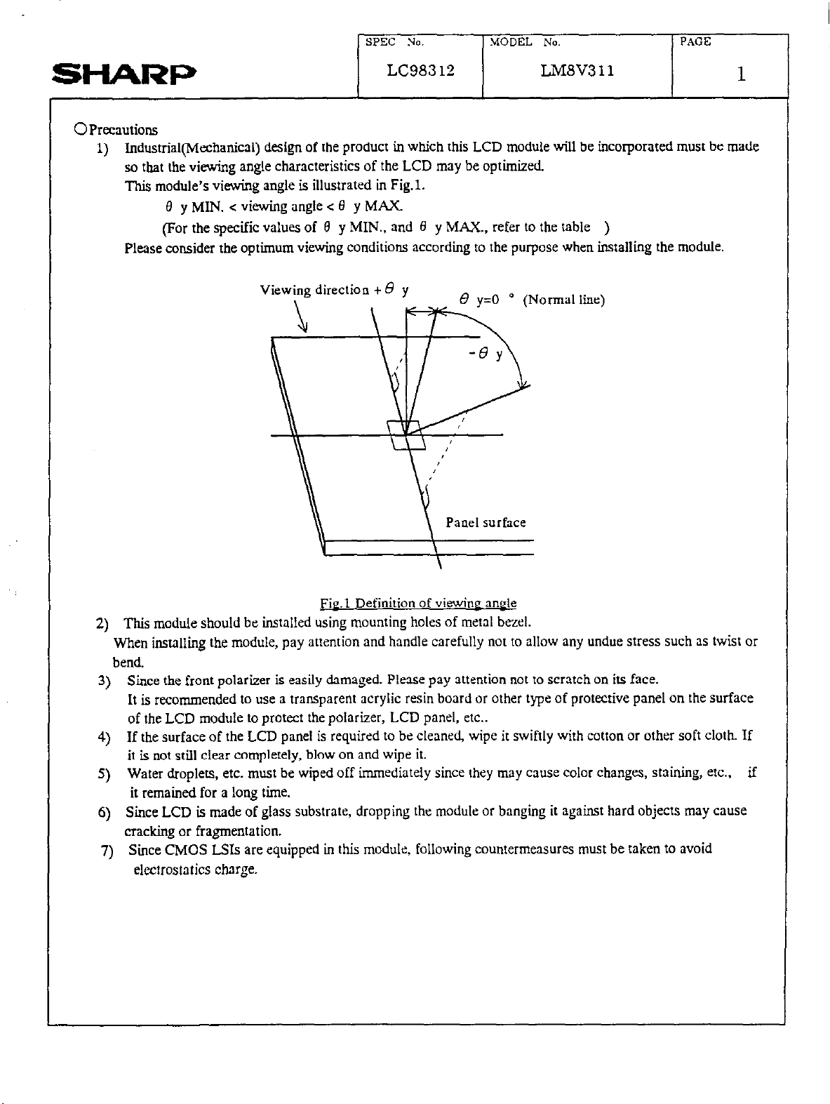
OPrecautions
1) Indusuial(Mechanica1) design of the product in which this LCD module will be incorporated must be made
so that the viewing angle characteristics of the LCD may be optimized.
This module’s vieGig angle is illustrated in Fig.1.
Please consider the optimum viewing conditions according to the purpose when installing the module.
LC983 12
f3 y MIN. < viewing angle < 0 y MAX
(For the specific values of 0 y MIN., and B y MAX., refer to the table )
Viewin;
g direction + 6 y
63 y=O ’ (Normalline)
LYiM8V311
,’
,’
>’
1
Panel surface
a
Fie.1 Definition of viewine anele
2) This module should be installed using mounting holes of metal bezel.
When installing the module, pay attention and handle carefully not to allow any undue stress such as twist or
bend.
3) Since the front polarizer is easily damaged. Please pay attention not to scratch on its face.
It is recommended to use a transparent acrylic resin board or other type of protective panel on the surface
of the LCD module to protect the polarizer, LCD panel, etc..
4) If the surface of the LCD panel is required IO be cleaned, wipe it swiftly with cotton or other soft cloth. If
it is not still clear completely, blow on and wipe it.
5) Water droplets, etc. must be wiped off immediately since they may cause color changes, staining, etc., if
it remained for a long time.
6) Since LCD is made of glass substrate, dropping the module or banging it against hard objects may cause
cracking or fragmentation.
7) Since CMOS LSIs are equipped in this module, following countermeasures most be taken to avoid
electrostatics charge.
Page 4
I
SPEC 210~ MODEI. x0. PAGE
SHARP
1 I operator
Electrostatic shielding clothes shall be had because it is feared that the static electricity is electrified to
human body in case that operator have a insulating garment.
2. Equipment
There is a possibility that the static electricity is charged to equipment which have a function of peeling
or mechanism of friction(EX: Conveyer, soldering iron, working table), so the
countermeasure(electrostaticearth:l X 10’ Q) should be made.
3. Floor
Floor is a important part to leak static electricity which is generated from human body or equipment.
There is a possibility that the static electricity is charged to them without leakage in case of insulating
floor, so the countermeasure(electrostatic earth:1 X 10’ Q) should be made.
4Humidity
Humidity of working room may lower electrostatics generating material’s resistance and have something
to prevent electrifying. So, humidity should be kept over 50 % because humidity less than 50 % may
increase material’s electrostatic earth resistance and it become easy to electrify.
5.Transportationlstorage
The measure should be made for storage materials because there is a possibility that the static electricity,
which electrify to human body or storage materials like container by friction or perling, cause the
dielectric charge.
6. Others
The laminator is attached on the surface of LCD module to prwent from scratches, fouling and dust.
It should be peeled off unhurriedly with using static eliminator.
And also, static eliminator should be installed to prevent LCD module from electrifying at assembling
line.
8) Don’t use any materials which emit gas from epoxy rcsin(amines’ hardener) and silicon adhesive
agent(dealcohol or deoxym) to prevent change polarizer color owing to gas.
9) Since leakage current, which may be caused by routing of CCFT cables, etc., may affect the brightness of
display, the inverter has to be designed taking the leakage current into consideration. Thorough evaluation of
the LCD module/inverter built into its host equipment shall be conducted, therefore, to ensure the specified
brightness.
10) Avoid to expose the module to the direct sun-light, strong ultraviolet light, etc. for a long time.
11) If stored at temperatures under specified storage temperature, the LC may freeze and be deteriorated.
If storage temperature exceed the specified rating. the molecular orientation of the LC may change to that of
a liquid, and they may not revert to their original state. Therefore, the module should be always stored at norm;
room temperature.
12) Disassembling the LCD module can cause permanent damage and should be strictly avoided.
LC98312
LM8V311
countemxasure
2
Page 5
SPEC No. MODEL No. PAGE
1
SHARP
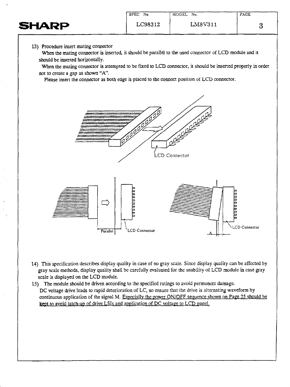
13) Procedure insert mating connector
When the mating connector is inserted it should be parallel to the used connector of LCD module and it
should be inserted horizontally.
when the mating connector is attempted to be fiied to LCD comxctor, it should be inserted properly io order
not to create a gap as shown “A”.
Please insert the coooector as both edge is placed to the connect position of LCD comxctor.
LC98312 LhI8V3 11
3
14) This specification describes display quality in case of no gray scale. Since display quality can be affected by
gray scale methods, display quality shall be carefully evaluated for the usability of LCD module in case gmy
scale is displayed on the LCD module.
15) The module should be driven according to the specified ratings to avoid permamnt damage.
DC voltage drive leads to rapid deteriomtion of LC, so ensure that the drive is alternating waveform by
continuous application of the signal M. ~sneciallv the Dower ON/OFF seauence shown on Page 25 should be
kept to avoid latch-w of drive LSIs and aonlication of DC voltaee to LCD onnel.
Page 6
SPEC No.
1
.MODEL No.
PAGE
SHARP
OConrenrs
l.Application
t.Coostruction and Outline
3.Mechanical Specifications
4Absolute Maximum Ratings
4-LElectrical absolute maximum ratings
4-Z.Enviroment Conditions
S.EIectricaI Specifications
.5-LEIectrical characteristics
.5-Z.Interface signals
6.Module Driving Method
6-LCircuit configuration
6-Z.Display face configuration
6-3.Input data and control signal
7.0ptical Characteristics
&Characteristics of Backlight
9.Suppiy voltage sequence condition
lO.Applicable inspection standard
ll.Lot Number
12.Touch Panel Specifications
LC98312
Page
5
6
7
8
10
16
18
23
25
26
27
LM8V3 11
4
Page 7
SPEC No. .MODEL No.
1
PAGE
SHARP
IApplication
This data sheet is to introduce the specification of L~M8V311. passive Matrix type Color LCD module.
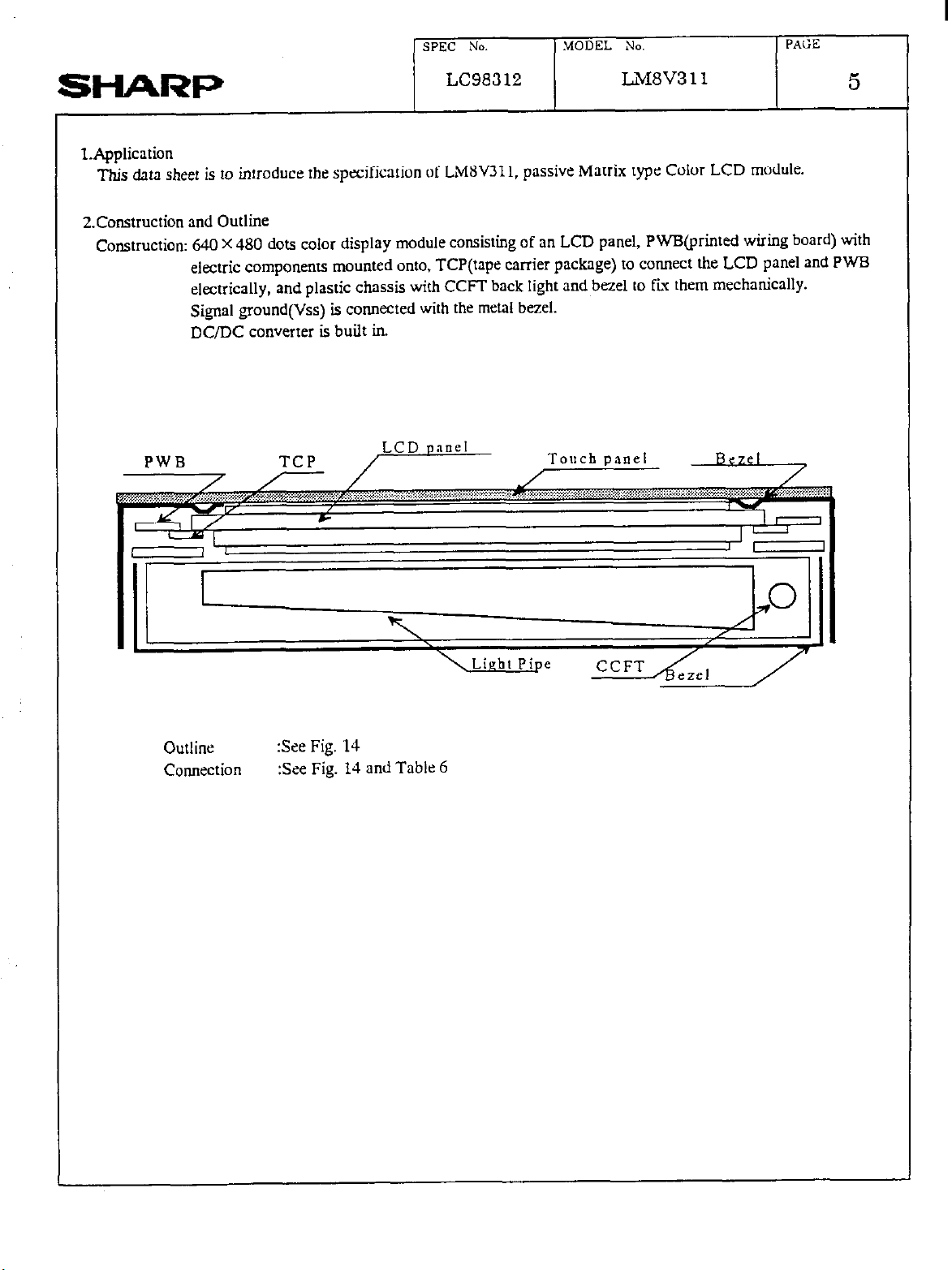
2.Cortstruction and Outline
Construction: 640 X 480 dots color display module consisting of an LCD panel, PWB@rixtted wiring board) with
electric comuonems mounted onto, TCP(tapc carrier package) to connect the LCD panel and PWB
electrically. and plastic chassis with CCFT back light and bezel to fix them mechanically.
Signal ground(Vss) is connected with the metal bezel.
DC/DC converter is built in.
PWB
/ r-------
I-M,
, 1
LC98312 LiiSV311
I I
Touch panel
,
I-
5
I
Outline
Connection
:See Fig. 14
See Fig. 14 and Table 6
,
*O
/
Page 8
SPEC No. .M”“EL No.
PAGti
SHARP
3Mechanical Specification
‘1 Due to the characteristics of the LC material; the colors vary with environmental temperature.
‘2 Negative-type display
Display data “H” : ON - transmission
Display data “L” : OFF -+ light isolation
4.Absolute Maximum Ratings
4-LElectrical absolute maximum ratings
LC983 12 Lh48V311
I I
6
I
PWam~t.X
Supply v0lt~ge(logic)
Input voltage
Vcon voltage
Table
Symbol MIN. MAX. unit
vm-vss
VU+
VCOO 0
0 6.0
-0.3 v,,+o.3
VDD
V
V
V
Remxk
Ta=25 “C
Ta=25 “C
Ta=25 “C
Page 9
SPEC No.
MODEL No.
PACE
SHARP
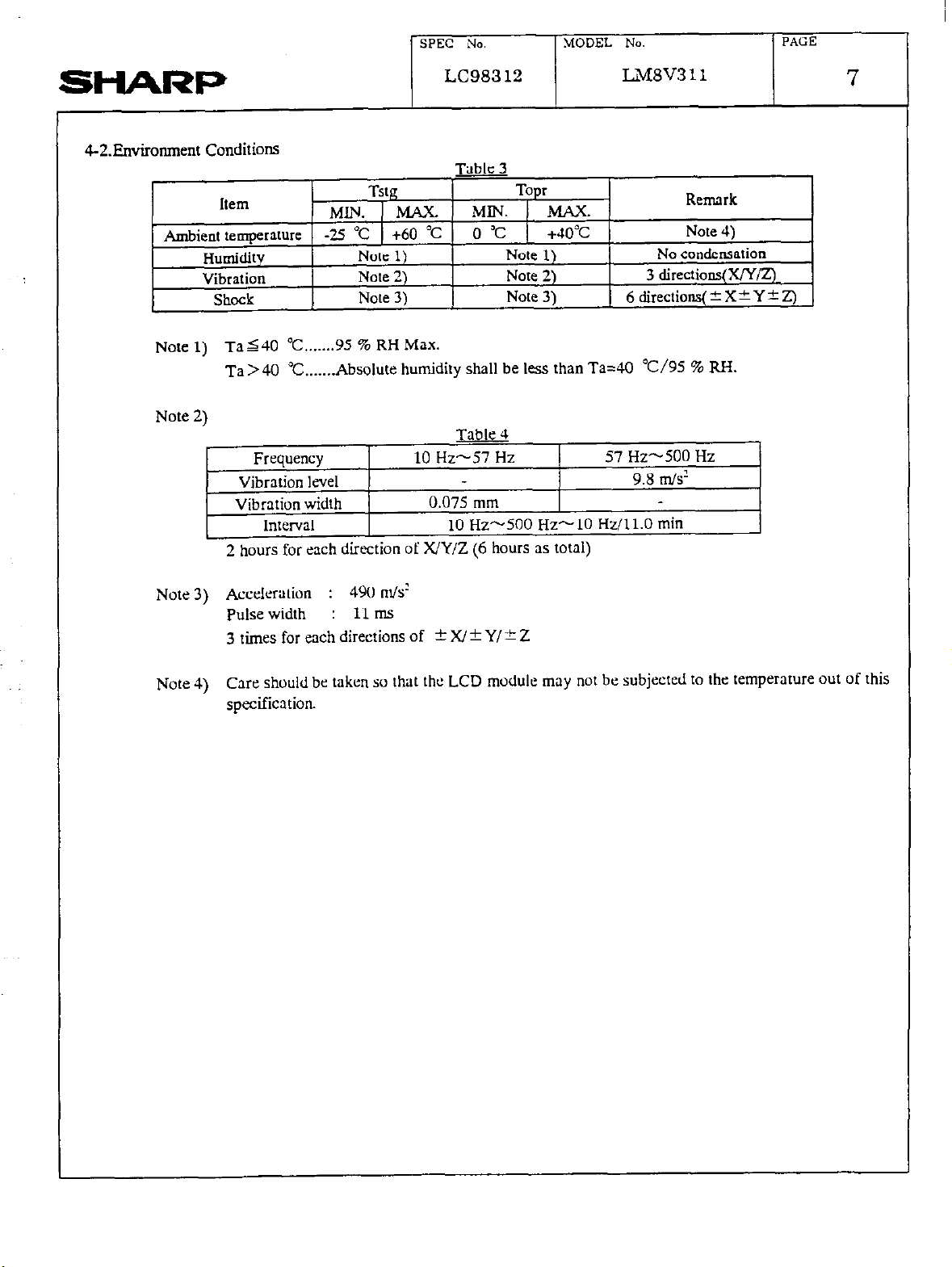
4-Z.Enviromnent Conditions
km
Ambient tempernture
Humiditv
Vibration
Shock Note 3)
Note 1) Ta540 “c . .._... 95 % RH Max.
Note 2)
LC983 12
I
Tsta
MIN. 1 MAX. MIN. ) MAX.
-2s “C 1 +60 “C
Note 1) Note 1)
Note 2) Note 2) 3 directions(XNlZ)
Ta>40 %.......Absolute humidity shall be less than Ta=40 “C/95 % RI%
Frequency 10 Hz-57 Hz 57 Hz-500 Hz
Vibration level 9.8 mls’
Vibralion width
Interval 10 Hz-500 Hz-10 Hz/ll.O min
2 hours for exh direction of WY/Z (6 hours as total)
0 % 1
Note 3)
w
0.075 mm
I
Topr
+JO%
LSfSV3 11
Remark
Note 4)
No condensation
6 directions( * X 2 Y + z)
T
I
7
Note 3) Acceleration : 490 m/s’
Pulse width : llms
3 times for each directions of +X/t Y/+ 2
Note 4) Care should be taken so that the LCD module may not be subjected to the temperature out of this
specification
Page 10

SPEC No. MODE!., No.
PAGE
SHARP
SXlectrical Specifications
5-l.Eiectrical characteristics
PWImtXeI
Supply voltage (Logic)
Contrast adjust voltage
Note 1) Under the following conditions.;
0 Immediately after the rise of V,,
@ Under the situation that DISP signal is on and kept steady : 0.15AX 100 u S
LC983 12 LiiSV3 11
-J-abJ&
Symbol
vm-vss
Vcon -v, Ta = 0 “C--JO%
Ta = O-40 “C (Note 1)
Ta=25 “C
Condilions Min.
VDD= 3.3 Vr. 10 %
PP.
3.0 3.3
0.8 1.95
: 0.6AX 1oms
8
l/tFRM=75 Hz
Max. unit
3.6
2.8
V
V
Note 2)
Note 3)
Frame frequency = 75 Hz, Vcon - Vss =max contrast voltage
Display pattern = all digits ON (DUO-7,DLO-7 = “H”)
q uoooooooonoonnoooo~
cl0000000n00000n0000G
COUOOCOOC!OOOOOOOO@@O
q
ClECIOOOUOOClOCiOUOOClO@
Frame frequency = 75 Hz. Vcon - Vss = max contrast voltage
Display pattern = black/white
00000000000000000000
stripe
pattern
n n n n n n n n n n n n n n n n n n n n
00G00000000000000000
n n n n n n n n n n n n n n n n n n n n
Page 11

SPEC No. ,XODEL No. PAGE
SHARP
Note 4) Contrast adjust voltage “Vcon-VW is transformed into the LCD driving voltage “V,” by following
circuit built in the LCD module.
LCD driving voltage “V,,
range by the temperature compensation circuit.
Temperature compensation circuit built in LCD module have been set obtain the optimum contrast under
following driving conditions.;
Take care that voltage for optimum contrast is changed under the different conditioa
Frame frequency : 75 Hz, Duty ratio : 11244 (an odd number frame), Ta = 25 “c
XThe above is the condition of the module settin?. not the electrical characteristics.
” is adjusted automatically according to the change of ambient temperature
LC98312 LiiSV3
,
I
11
VDD
Control signal
VLCD
vcm-
9
Page 12

SPEC ?Io.
MODEL No. P.GE
SHARP
5-2.lnterface signals
OCNl
LC983 12
Table 6-l
LMSV3 11
10
OCN2
13
I4
Table 6-2
I
NC
VCOD
I I
Contrast xljustment voltage
Page 13

SPEC No.
MODEL No.
PAGE
SHARP
OCCFr
5-3.CoMectors
OLCD
OCCFT
Except
I I
Table&3
Pin No
1
2
3 HV
Used
COM6!CtOr
Correspondable connector
Used coonector
Correspondable connector
above cotmector shall be out of guaranty.
Symbol Description
GND
NC
Ground line (from Invener)
High voltage line (from Inverter)
: CNl 53X1-1510(Molex)
: CNl 51021-lSOO(Molex)
:QZ-19~3FOl(Honda Tsushin kogyo)
:QZ-lY-A3MYL#OZ(Honda Tsushin kogyo)
LC98312
NC
LMSV311
Level
CN2 53261-1410(Molex)
CN2 51021-1400(Molex)
11
Page 14

SPEC No.
MODEL No.
PAGE
SHARP
LC98312
Lw3v3 11
640 x 3 (RGB)
x 480 dots
12
-I\
(480.1) (480,2)
(480,639) (480,640)
_.--_.-_..
m Upper SEG Drcvers . Upper d.ra(DUO-7)
- Lowvsr SEF Drivers .Lowucr data(DLO-7)
Page 15

SPEC No. .MclDEl. No.
P.GE
SHARP
LC98312 LkfSV311
13
1
DL5
E
k?t
DLO
I
-fuI--L---l-rL
l
Electric.4 and optical chnr~ckrislics are spccilied by above condition.
Fk. 3 Data innut riminecharr
Page 16

SPEC No.
.MODEt. No.
PAGE
SHARP
YD At-
LP /
<
t
"IS
i+--+
l-
LC98312
t
FR"
t
H""
3
t
LIE
N
Q&
LAmv3
11
t
L""
14
XCK
DUO-7
DLO-7
<
t
LS
J t
<
t,
-4-t-, ,
LH
V,H = 0.8 v,,,
VIL = 0.2 V,D
tr
Page 17

SPEC No.
,
1
.MODEL No.
PAGE
SHARP
LC98312
Table 7 interface timine rating
IA48V3
Ta=2.5 “c,VDD=3.3 ‘.‘*lO %
11
15
‘1 When LCD module is operated by high speed of XCK(ShiIt clock), (tcr - t,,, -twcKL) /2 is maximum,
‘2 According to our experiments, frame cycle of 8.33 ms Min. or frame frequency of 120 Hz Max. will
demonstrate optimum display quality in terms of Hicker and “shadowing”. But since judgment of display
quality is subjective and display quality such as “shadowing” is pattern dependent, it is recommended
that decision of frame frequency, to which power consumption of the LCD module is proportional, be made
based on your own through testing on the LCD module with every possible patterns displayed on it
:.
X Th
e imervnls
The intervals must be 70 in s Max.
of one LP fall and nrxt must he nlwnvs the sane, and LPs must he innut continuouslv.
Page 18

SPEC No. .MODEL No. PAGE
SHARP
6. Module Driving Method
6-l. Circuit configuration
Fig.10 shows the block diagram of the module’s circuitry.
6-2. Display face configuration
The display consists of 640 X 3(R,G,B) X 480 dots as
The interface is single panel with double drive to be driven at 1/244duty ratio.
6-3. Input data and control signal
The LCD driver is 240 bits LSI, consisting of shift regisrers, latch circuits and LCD driver circuits. Input data
for each row 640 X 3 (R,G,B) will be sequentially transferred in the form of 8 bit parallel data through
shift registers from top left of the display together with clock signal (XCK).
When input of one row 640 X 3 (R,G,B) is completed, the data will be latched in the form of parallel
data corresponding to the signal electrodes by the falling edge of latch signal (LP) then, the corresponding
drive signals will be transmitted to the 640 X 3 lines of column electrodes of the LCD panel by the LCD
drive circuits.
At this time, scan start-up signal (I’D) has been transferred from the scan signal driver to the 1st TOW of scan
electrodes, and the contents of the data signals are displayed on the 1st row of the display face according to
the combinations of voltages applied to the scan and signal electrodes of the LCD. While the data of 1st row
are being displayed, the data of 2nd row arc cntercd. When data for 640 X 3 dots have beon transferred, they
will be latched by the falling edge of LP, switching the display to the 2nd row.
LC98312 LiiSV311
shown
in Fig. 2..
16
Such data input will be repeated up to the 244th row of each display segment, from upper row to lower
rows. to complete one frame of display by time sharing method.
Simultaneously the same scanning sequence occur at the lower panel.
Then data input proceeds to the next display frame.
YD generates scan signal to drive horizontal electrodes.
Since DC voltage. if applied to LCD panel, causes chemical reaction in LC materials, causing deterioration of
the materials, drive wave-form shall be inverted at ewry display frame to prevent the generation of such DC
voltage.
Control signal ,M plays such a role.
Because of the characteristics of the CMOS driver LSI. the power consumption of the display module goes up
with the
To minimize data transfer speed of XCK clock the LSI has the system of transferring 8 bit parallel data
through the 8 lines of shift registers.
Thanks to this system the power consumption of the display module is minimized.
In this circuit configuration, 8 bit display data shall input to data input pins of DUO-7 and DLO-7.
Furthermore, the display module has bus linr system for data input to minimizc the power consumption with
data input terminals of each driver LSI being activated only when relevant data input is fed.
clock
frequency of XCK.
Page 19

SPEC No. MODEL. No. PAGE
SHARP
Data input for column electrodes and chip sekc~ of
The driver LSI at the left end of the display face is first selected, and the adjacent driver LSI right next side
is selected when data of 240 dot (3OXCK) is fed. Ths process is sequentially continued until data is fed to
the driver LSI at the right end of the display face. This process is followed simultaneously both at the top
bottom column
Thus data input will be made through 8 bit bus line sequentially from the left end of the display face.
Since this display module contains no refresh RAM, it requires the above data and timing pulse inputs even for
static display.
The timing chart of input signals are shown in fig. 4 and Table 7
drivers LSI’S.
LC98312 Li’dSV3 11
driver
LSI are made as follows:
17
and
Page 20

SPEC No.
.MOL)EL N”.
I’AC E
SHARP
LC98312 LMSV3 11
1 , ,
7.0ptical Characteristics
Followittg spec are based upon the electrical measuring condirions, on which the contrast of perpendicular
direction(B x= fl y=O ’ )willbeMAX..
Ta = 25 “C, V,,= 3.3V, Vcon-V, = Vma,
Note 1) The viewing angle range is defined as shown Fig.5
18
tex
Note 2)
Note 3)
tex
-BY
-BY
Fir.5 Definition of Viewine AnpIe
Contrast ratio is defied as follows:
Co Luminance(brightness) all pixes “White” at Vmax
= Luminance@tightness) all pixes “dark ” at V~ZLX
Vmax is defied in Fig.7.
The response characleristics of photo-detector output are measured as shown in Fig.9, assuming that input
signals are applied so as to select and deselect the dot to be measured, in the optical characteristics test
method shown in Fig.8.
Page 21

I
SPEC No.
PAGE
SHARP
LC98312
19
Measuring Spot Size : @ 10 mm
B x : Angle from “normal” to viewing surface rotated about the horizontal axis
0 y :
I I
Angle from “normal” to viewing surface rotated about the vertical axis.
Fi.z.6 Optical Characteristics Test Method I
' Vcon-vss (V)
Vmax .
Fie.7 Definition of Vmax
Page 22

SPEC 30.
MODEL No.
PAGE
SHARP
(Response Measurement)
Ta = 25 “C
In dark mom
LCD Module
~, Era
,-
,’
,‘1
%
LC983 12
,’
’ ,’
LTTSV3 11
TOPCON BM7 + quartz fiber
_’
\,? ,\
L
20
(Measuring spot size : ~3 10 mm, Measuring Field : 2 ’ )
Fig. 8 Optical Characteristics Test Method II
Page 23

SPEC No. .MODEL iNo.
PAOE
SHARP
T 1
[Drive waveform]
LC983 12 LM8V3 11
11244 Duty Ratio
21
1
-Non-select
wavefom
[Responce waveform]
2-r
,
Fie.9 Definition of Resmnse time
rd
\
r r: Risetitne
7 d: Decaytime
I
/\
Page 24

SPEC No.
MODEJ. No.
PAGE
SHARP
ILO-DL7
YCK
LP
I
I
I-
Bias generator
Protection circuit
1 DISP
&
LC983 12
LII8V3 11
22
-
,
-
jEG Drivers (Upper)
i b=-
(2,640)
i
R B
m
I
r
240,l)
)
241,t) (241,640)
640 X 480 DOTS LCD PANEL
(24~,fj4_0?
T
1(460,1)
(480,640) 1
I
VSS
VDD
‘:
Converter
Vcon
CCFT
Inverter
,1..--............-.............~-.........-.--..
Temperature
Compensation
ic. 0 Circuit block diwra
I
1
I ?T M
I 1
I
I
SEG Drivers (Lower)
T
I
I
Page 25

SHARP
8.Cbaracteristics of Backlight
The ratings are given on condition that the following conditions are satisfied.
1) Rating(Note)
Parameter
Brightness
2)
Measurement circuit : CXA-LOSOS-VJL(TDK)
3) Measurement equipment :
4) Measurement conditions
4-l. Measurement circuit voltage :
4-2. LCD: All digits WHITE, VDD= 3.3 V, Vcon-VSS = Vmax, DUO-7=“H”(Wbite),DL0-7=“H”(White)
Fmme Frequency 75 Hz
4-3. Ambient temperature : 25 %
Measurement shall he executed 30 minutes after turning on.
5) Used lamp : KCA1344SH(WEST ELECTRIC Co.)
Used cable : UL3579,AWG#26
(NISSEI ELECTRIC CO.,LTD “I- SUMITOMO ELECTRIC INDUSTRIES LTD.)
5-l.
MIN.
38
BM-7 (TOPCON Corporation)
DC = 12.0 V,
LC98312
Table9
TV. MAX.
55
(at IL = 3.0 InArms)
at primary side
LMSV3 11
23
Unit
cd/m’
~a=25 “C
( 1050 VrtIls
Within no conductor closed. (CCFf “my)
*1 It is recommended that IL be not mow than 4.0 mArms so that heat radiatic
may least affect the display quality.
‘2 Power consumption excluded invertrr loss.
‘3 The circuit voltage of the invertcr should be designed to have some margin. because VS may be
increased due to the leak current in use of the LCD module.
‘4 Average life time of CCFf will be decreased when LCD is operating at lower temperature.
. ~
Ta= 0 “C ‘3
h Ta=25 “C
Ta= 0 “C ‘4
h
m of CCm backlight
Page 26

SPEC No.
MODEL No. PAGE
SHARP
5-2. Operating life
(NOTE) Rating are defied as the average brightness inside the viewing area specified in Fig.11.
LC98312 LiiSV3 11
The operating life time is 25 000 hours or more at 3.0 tn.&.
(Operating life with CXA-LOSO5-VJL or equivalent.)
The inverter should meet the following conditions to keep the specified life time of used lamp;
-Since, symmetric waveform without spike in positive and negative
-Output frequency range: 30 kHz-70 kHz
Make sure the operating conditions by executing the bum-in enough time.
The operating life time is defied as having ended when any of the following conditions occur; 25 2 1°C
-when the voltage required for initial discharge has reached 110 % of the initials value.
-When the illuntinence quantity of light has decreased to 50 % of the initials value.
ACTIVE AREA
/
24
1
120
240
360
dots
a,-
_.....
:
320 480 dots
Fie.11 Mcasurine ooints 11-5)
Page 27

SPEC x0. MODEL No.
PACE
SHARP
9.Supply voltage sequence condition
<
&
VDD
YD
LP
YCK
DATA
DISP
VDD
‘VSS”
-
LC98312
I
1500 ms MIN. (NOTE 1)
I I
Interface ttmtttg acttve operation
LM8V311
I
>
e 1s MIN
1
25
(NOTE 1)
(NOTE 2) Before DISP rise up. the signals of YD,LP,XCK,DATA must be input, and the above condition of “a”
Symbol
a 0 ms MIN.
b
c
d
Power ON/OFF cycle time. All signals and power line shall be in accordance with above sequence in
case of power ON/OFF.
must be satisfied. The signals which comply with the interface timing in Fig.3,Fig.4, and table 6, must
be input.
POWER ON
Allowable value
1sMAX.
-
50 m MIN.
100 ns MAX.
10 ms MAX.
( 10 msMIN. )
g
-
Page 28

SPEC No. .MODEL No.
1
PAGE
SHARP
lO.Applicable inspection standard
The LCD module shall meet the following inspection standard : S-U-037
ll.Lot Number
Lot number is shown at the position mentioned in Fig.13 in accordance with the following numbering rule.
Serial number(Missing number exist)
Productloo month(A=Jan.,B=Feb:“.L=Dec.)
pamp’e) L Production year
LC98312 LMSV311
26
m
r
\Model and Serial number
Page 29

SPEC No.
.MODEL No.
PACE
SHARP
12.Touch Panel Specifications
12.1. Rating
12.1.1. Maximum voltage and current: 7V 24mA
X2.1.2. Operating temperature: -10°C
12.1.3. Storage temperature: -40”C270”C(Humidity from 20% to 90%. No dew condensation)
12.2. Electrical Performance
12.2.1. Resistance between terminals:
Direction “X”(Film side) : 350-900 Q(TYP. 480 Q)
Direction “Y’(Glass side): 450-1100 Q(TYP. 630 Q)
12.2.2 Linearity
Direction “x”: 1.5% or less
Direction “Y? 1.5% or less
12.2.3.
12.2.4. Chattering: 1Omsec or less
12.3. Mechanical Performance
12.3.1. Input: finger or special stylus pen
12.32. Activation Force:
Insulation
Input with finger: 80g or less (typ.lSg)
Input with stylus: 8Og or less (typl5g)
resistance: DC 25V and 201M 51 or more
--SO”C(Humidity from 20% to 90%, No dew condensation)
LC983 12 LX8V3
11
27
12.3.3. Surface hardness: Hardness of pencil 3H or more
12.4. Optical Performance
12.4.1. Optical clarity: 77%(MIN.) 79%(TyP.)
12.5. Correspondable connector
04FFS-SP-TF(JST: SMT,Non-ZIF type) or equivalent
Page 30

IC-Ol<O. 6
B :2.5to.l3
68: 1. 5to. 5
A :2.5*0.6
AA:1.5*0.5
3) OBLIQUITY OF DISPLAY AREA
21 TOLERANCE Y-DIRECTION
\TOUCH PANEL 11 TOlERANCE X-DIRECTION
159. 4x120. 1
IUCH PANEL ACTIVE AREA
100. 67fl ( I/F mvmm tenon
Toucti PANEL IIF CABLE
I NTERFAChCiNNECTOR
CN1:53261-1510(MOLEX)
<PIN LAYOUT>
(2) CN2:53261-1410(MOLEx)
I
 Loading...