Page 1

Ordering number: EN 2658A
PMOS LSI
LM8562
Digital Alarm Clock
Overview
The LM8562 is a digital clock-use LSI having features such as
easy setting, two alarms. Since the LM8562 is designed to be
able to direct drive an LED panel of duplex type, the package
in which the LM8562 is placed is a 28-pin shrink DIP with a
small mounting area.
Features
(1) Duplex LED display (LM8560-use LED panel usable)
(2) Two alarms on chip (600Hz, 1200 Hz)
(3) Up, down/fast, slow time setting available (easy setting)
(4) 12/24-hour mode, 50/60 Hz selectable (provided that it is
impossible to select the combination of 24-hour mode and
60 Hz)
(5) On-chip CR oscillator for backup use at the time of power
failure
(6) Power failure indicator
(7) 59-minute alarm/sleep timer
(8) 6-minute snooze function
(9) Radio output function
(10) P-channel ED MOS
(11) Pin 28 dual-in-line shrink package
(12) Wide operating voltage/operating temperature range
V
= –14 to –8 V / –20 to +70°C
DD
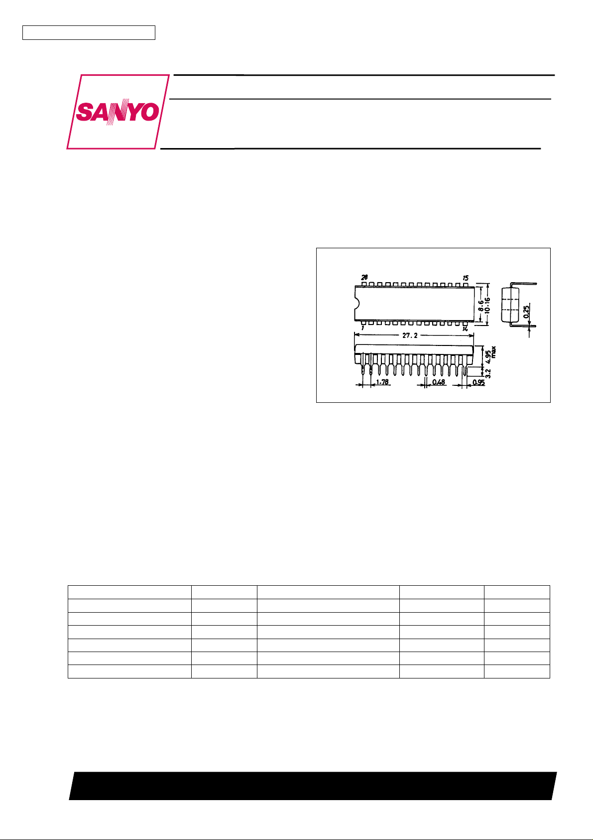
Package Dimensions
unit : mm
3029A-DIP28S
[LM8562]
SANYO : DIP28S
Specifications
Absolute Maximum Ratings at Ta = 25°C, VSS=0V
Parameter Symbol Conditions Ratings Unit
Supply voltage V
Input voltage V
Output voltage V
Allowable power dissipation Pd max Ta = 70°C 0.7 W
Operating temperature Topr –20 to +70 °C
Storage temperature Tstg –55 to +125 °C
max –17.0 to +0.3 V
DD
IN
OUT
–17.0 to +0.3 V
–17.0 to +0.3 V
SANYO Electric Co.,Ltd. Semiconductor Bussiness Headquarters
TOKYO OFFICE Tokyo Bldg., 1-10, 1 Chome, Ueno, Taito-ku, TOKYO, 110 JAPAN
D2897HA (II)/6209TA No.2658-1/7
Page 2

LM8562
Allowable Operating Conditions at Ta = –20 to +70°C, VSS=0V
Parameter Symbol Conditions min typ max Unit
Supply voltage V
Standby voltage V
Input high-level voltage V
Input low-level voltage V
Input high-level voltage V
Input low-level voltage V
Input high-level voltage V
Input mid-level voltage V
Input low-level voltage V
Input high-level voltage V
Input low-level voltage V
DD
ST
1 50/60 Hz INPUT pin VSS–1 V
IH
1 VDD+2 V
IL
2 CR OSC pin VSS–1 V
IH
2V
IL
3 3-level input pins VSS– 0.7 V
IH
IM
3V
IL
4 Input pins other than the above VSS–2 V
IH
4V
IL
Input level hold time tH 10 ms
Input chattering time tC 10 ms
Electrical Characteristics atTa=25±2°C, VSS=0V,VDD= –12 V
Parameter Symbol Conditions min typ max Unit
Output high-level current I
Output OFF-state leakage current I
Output high-level current I
Output OFF-state leakage current I
Output high-level current I
Output OFF-state leakage current I
OH
OF
OH
OF
OH
OF
Operating frequency fop 50/60 Hz INPUT pin DC 2000 Hz
Input high-level current I
Input low-level current I
Input high-level current I
Input low-level current I
Input high-level current I
Input low-level current I
Pull-down resistance R
Pull-up resistance R
Operating current I
Power failure detect circuit V
IH
IL
IH
IL
IH
IL
PD
PU
DD
BU
OSC stability f
OSC accuracy f
OSC frequency f
OSC
Note 1 : The allowable segment current drain is 78 mA max. for AM & 10’SHR ag & de and 39 mA max. for other than AM &
10’SHR ag & de in the range of power dissipation 700 mW.
AM & 10’SHR ag & de pin,
1
V
OUT=VSS
1V
OUT=VDD
Segment output pins other than the
2
above, V
2V
OUT=VDD
ALM-1, ALM-2, RADIO OUTPUT pin,
3
V
OUT=VSS
3V
OUT=VDD
1VIH=V
1VIL=V
2 CR OSC pin, VIH=V
2VIL=V
3 3-level input pins, VIH=V
3VIL=V
3-level input pins, VIN= 1/2 V
VIN= 1/2V
– 2.0 V
OUT=VSS
– 2.0 V
SS
DD
DD
DD
DD
– 2.0 V
SS
SS
DD
Output : No load 2 8 15 mA
VDD=–9V±10% –10 10 %
S
VDD= –9 V –10 10 %
A
R = 180 kΩ, C = 3300 pF 2400 Hz
–14 –8 V
–7.5 V
V
SS
V
SS
+2 V
DD
SS
V
1/2 VDD– 1 1/2 VDD+1 V
DD
VDD+1 V
SS
+2 V
DD
V
32 (Note1) mA
20 µA
16 (Note1) mA
20 µA
2mA
10 µA
10 µA
–10 µA
10 µA
60 µA
20 120 µA
–120 –20 µA
1.0 MΩ
0.8 MΩ
–7.5 –5.0 V
No.2658-2/7
Page 3

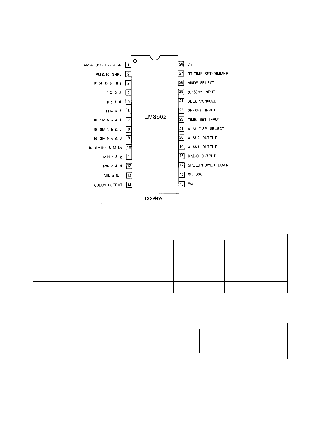
Pin Assignment
LM8562
Pin Functions
1. 3-Level Input Pins
No. Pin Name
17 SPEED/POWER DOWN Test mode Normal Power-down mode
21 ALM-DISP SELECT Alarm 2 display & setting NOP Alarm 1 display & setting
22 TIME SET INPUT Slow-down (AC = fast-down) NOP Slow-up (AC = fast-up)
23 ON/OFF INPUT ON NOP OFF
24 SLEEP/SNOOZE Sleep display & sleep-in NOP Second display & snooze-in
26 MODE SELECT 24-hour mode, 50 Hz 12-hour mode, 50 Hz 12-hour mode, 60 Hz
27 RT-TIME SET/DIMMER Time setting inhibit
Dimmer display
V
SS
NOP : No operation
AC : Pulse input
2. Input/Output Pins
No. Pin Name
18 RADIO OUTPUT — When not used
19 ALM-1 OUTPUT — Alarm1 OFF
20 ALM-2 OUTPUT — Alarm2 OFF
16 CR OSC 1-pin OSC circuit
V
SS
3. Input Pins
No.25 50/60 Hz INPUT = 50 Hz or 60 Hz clock signal input
No.15, 28 V
SS,VDD
= Power supply pin
Input Level
OPEN V
Timer setting inhibit
Normal display
Input Level
DD
Time setting enable
Normal display
V
DD
No.2658-3/7
Page 4

4. Output Pins
LM8562
No. Pin Name
1 AM & 10’SHR ag & de AM 10’SHR ad 10’SHR eg
2 PM & 10’SHR b PM 10’SHR b
3 10’SHRc&HRe HRe 10’SHR c
4 HRb&g HRg HRb
5 HRc&d HRd HRc
6 HRa&f HRf HRa
7 10’SMINa&f 10’SMIN a 10’SMIN f
8 10’SMINb&g 10’SMIN b 10’SMIN g
9 10’SMINc&d 10’SMIN c 10’SMIN d
10 10’SMIN e & MIN e MIN e 10’SMIN e
11 MINb&g MINg MINb
12 MINc&d MINd MINc
13 MINa&f MINf MINa
14 COLON OUTPUT COLON —
12
Drive Phase
Display Mode
Select Pin
ALM-DISP SELECT SLEEP/SNOOZE INPUT 1234
OPEN OPEN Time display
V
DD
V
SS
OPEN (V
OPEN (V
)V
DD,VSS
)V
DD,VSS
OPEN Alarm 1
OPEN Alarm 2
SS
DD
Display Mode
AM/PM
10’s hour
AM/PM
10’s hour
AM/PM
10’s hour
Sleep Unlit 0
second display Unlit Minutes
Hour
Hour
Hour
Digit No.
minutes
minutes
minutes
minutes
seconds
10’s
10’s
10’s
10’s
10’s
Seconds
Minutes
Minutes
Minutes
Minutes
Operation Description
1. Segment Output
The duplex LED panel can be direct driven by 13 segment output pins.
(Compatible with LM8560-use LED panel)
2. Colon Output
LED panel
Colon
The drive phase is phase 1. The colon always flashes at 1 Hz rate.
3. OSC Circuit
By connecting a resistor and a capacitor with the CR INPUT pin, a 2.4 kHz OSC circuit is formed. The clock signal
generated by the 2.4 kHz OSC circuit is used in the following cases.
(1) Used as the clock signal for the time counter, instead of 50/60 Hz INPUT, when the power-down mode is entered.
(2) Alarm sound (1200 Hz or 600 Hz) at the alarm signal output mode
(3) 1/25 duty clock signal while the dimmer is in operation
4. Power-Down Mode
(1) Since the backup OSC circuit holds the current time, the LM8562 starts operating immediately.
(2) The snooze function stops operating.
(3) The RADIO OUTPUT pin is brought to the OFF state.
(4) The control input is inhibited (except the following).
.
OFF INPUT
.
ALARM/SLEEP TIME SET INPUT at the time setting enable mode
No.2658-4/7
Page 5

LM8562
5. Alarm
The LM8562 contains two alarms on a 24-hour basis.
Alarm 1 ..... Superposition of 600 Hz and 1 Hz
Alarm 2 ..... Superposition of 1200 Hz and 1 Hz
6-minutes snooze
The alarm output duration time is 59 minutes. The 59-minute duration counter is common to the alarm 1, alarm2, and sleep
timer.
6. Time Setting, Dimmer
The 3 level input RT-TIME SET/DIMMER INPUT pin provides the following functions.
RT-TIME SET/DIMMER INPUT Pin Input Functions
V
DD
OPEN Time setting inhibit, normal display
V
SS
The 3-level input TIME-SET INPUT pin provides the following operations.
TIME-SET INPUT Pin Input Operations
V
DD
OPEN No operation
V
SS
AC (50/60 Hz or more) Fast-up
DC (20 ms min.) Slow-up
AC (50/60 Hz or more) Fast-down
DC (20 ms min.) Slow-down
Time setting enable, normal display
.
Time, alarm time, sleep timer duration time setting enable
.
Time setting enable (except power-down mode)
Time setting inhibit, dimmer display
.
Display brightness 50 Hz mode: 1/24 duty
60 Hz mode: 1/20 duty
Setting Contents
1 Fast-up/down 50/60 Hz rate
2 Slow-up/down Immediately incremented/decremented ±1 and counted up/down ata2Hzrate 0.5 to 1.0 second later
7. ON/OFF INPUT Pin
The 3-level input ON/OFF INPUT pin acts on the ALM-1, 2 RADIO OUTPUT pins as shown below.
Output Pin ON-State Condition
ALM-1 OUTPUT Alarm 1 setting time = Current time Snooze-in
ALM-2 OUTPUT Alarm 2 setting time = Current time Snooze-in
RADIO OUTPUT ON/OFF INPUT = V
(ON-state indicator : ON state)
Sleep-in
(Sleep indicator : ON state)
8. Sleep, Snooze Timer
The 3-level input SLEEP/SNOOZE INPUT pin operates as shown below.
SS
Pause
Conditions
—
—
OFF-State Conditions
.
ON/OFF INPUT = V
.
ON/OFF INPUT = V
.
Sleep-in
.
59 minutes after the alarm 1 is turned ON
.
ALM-1 OUTPUT = V
.
ON/OFF INPUT = V
.
ON/OFF INPUT = V
.
Sleep-in
.
59 minutes after the alarm 2 is turned ON
.
ALM-2 OUTPUT = V
.
ON/OFF INPUT = V
.
Power-down mode
.
Sleep-in
(On-state indicator : OFF state)
.
ON/OFF INPUT = V
.
ON/OFF INPUT = V
.
Power-down mode
(Sleep indicator : OFF state)
SS
DD
DD
SS
DD
DD
DD
SS
DD
SLEEP/SNOOZE INPUT Pin Input Operation
V
(20 ms min.) Snooze-in & seconds display mode
DD
OPEN No operation
V
(20 ms min.) Sleep mode
SS
.
The alarm stops functioning for 6 to 7 minutes.
.
Seconds display
.
The sleep counter is set to operate for 59 minutes.
.
Counted down automatically ata2Hzrate 1.5 to 2.0 seconds later
.
Fast/slow, up/down time setting available
No.2658-5/7
Page 6

LM8562
9. 50/60 Hz INPUT Pin
The LM8562 contains a Schmitt circuit so that a simple CR filter can be used to remove the noise of commercial frequency
50/60 Hz.
10. 12/24-Hour Mode, 50/60 Hz Select
The 3-level input MODE SELECT pin provides the following combinations.
MODE SELECT Pin Input Select
V
DD
OPEN 12-hour mode & 50 Hz
V
SS
Sample Application Circuit
12-hour mode & 60 Hz
24-hour mode & 50 Hz
No.2658-6/7
Page 7

Block Diagram
LM8562
No products described or contained herein are intended for use in surgical implants, life-support systems,
aerospace equipment, nuclear power control systems, vehicles, disaster/crime-prevention equipment and the like,
the failure of which may directly or indirectly cause injury, death or property loss.
Anyone purchasing any products described or contained herein for an above-mentioned use shall:
1 Accept full responsibility and indemnify and defend SANYO ELECTRIC CO., LTD.,its affiliates, subsidiaries and
distributors and all their officers and employees, jointly and severally, against any and all claims and litigation
and all damages, cost and expenses associated with such use:
2 Not impose any responsibility for any fault or negligence which may be cited in any such claim or litigation on
SANYO ELECTRIC CO., LTD., its affiliates, subsidiaries and distributors or any of their officers and employees
jointly or severally.
Information (including circuit diagrams and circuit parameters) herein is for example only; it is not guaranteed for
volume production. SANYO believes information herein is accurate and reliable, but no guarantees are made or
implied regarding its use or any infringements of intellectual property rights or other rights of third parties.
This catalog provides information as of December, 1997. Specifications and information herein are subject to change without notice.
No.2658-7/7
 Loading...