

Page 1
PRELIMINARY
LM8300/LM8400/LM8500
Four Wire Resistive Touchscreen Controller with
Brownout
General Description
The LM8300/8400/8500 is a 4-wire resistive touch screen
controller. The controller samples and drives the touch
screen without the need of any external hardware. The built
in 10-bit A/D provides a maximum of 500 coordinate pairs
per second (cpps). The data sampled from the touch screen
is sent out on the UART at a speed of 38400 bps.
The controller has a power-saving mode which causes the
controller to self-power down when no touch is detected on
the touch screen for a specified amount of time. In the
Devices included in this datasheet:
Device
LM8300 3, 5 V 2.7 to 2.9 V 3.27 MHz 18
LM8400 3, 5 V No Brownout 3.27 MHz 18
LM8500 5 V 4.17V to 4.5V 3.27, 10 MHz 18
Operating
Voltage
Brownout
Voltage
Operating
Frequency
self-power down mode, the current drawn is typically less
than 2 µA. The device resumes normal operation when a
touch is detected on the touch screen or communication is
detected on the UART. In addition to the self-power down
mode, the controller can be disabled by pulling the SHUTDOWN pin low. The controller resumes normal operation
when the SHUTDOWN pin is tristated or pulled high.
The controller has an internal non-volatile memory storage
element to store configuration data such as calibration points
or controller configurations.
I/O
Pins
Packages Temperature
44 LLP, 44 PLCC,
48 TSSOP
44 LLP, 44 PLCC,
48 TSSOP
44 LLP, 44 PLCC,
48 TSSOP
LM8300/LM8400/LM8500 Four Wire Resistive Touchscreen Controller with Brownout
October 2002
0˚C to +70˚C
0˚C to +70˚C
0˚C to +70˚C
Features
KEY FEATURES
n Supports 4 wire resistive touch panels
n Low power standby current typically less than 2 µA at
5.5V
n Maximum speed of 500 coordinate pairs per second
n Automatic wake up and return to standby
n 10 bit A/D
n On-chip touch screen current drivers - no external driver
required
n UART interface
n Controller configurations are stored in the internal
non-volatile storage element
n Touch pressure can be measured
APPLICATIONS
n Personal Digital Assistants
n Smart Hand-Held Devices
n Touch Screen Monitors
n Point-of-Sales Terminals
n KIOSK
n Pagers
n Cell Phones
COP8™is a trademark of National Semiconductor Corporation.
© 2002 National Semiconductor Corporation DS200372 www.national.com
Page 2
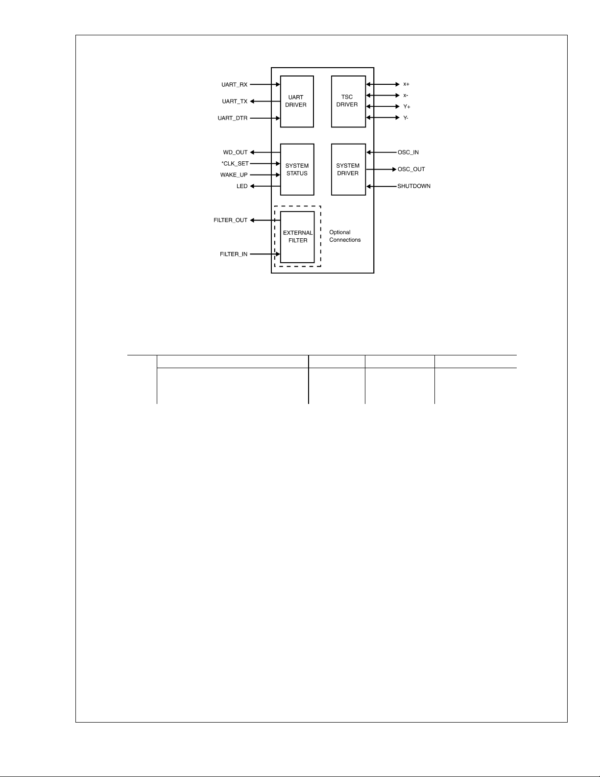
Block Diagram
LM8300/LM8400/LM8500
*
This pin is available in the LM8500. It is unused in the LM8300/LM8400.
Ordering Information
Part Numbering Scheme
LM 8300 H VA 9
Family and Feature Set Indicator No. Of Pins Package Type Temperature
8300 = Low Brownout Voltage
8400 = No Brownout
8500 = High Brownout Voltage
H=44Pin
I=48Pin
LQ = LLP
MT = TSSOP
VA = PLCC
20037201
9 = 0 to +70˚C
www.national.com 2
Page 3

Table of Contents
General Description ............................................................................................................................................ 1
Features ............................................................................................................................................................. 1
Block Diagram .................................................................................................................................................... 2
Ordering Information .......................................................................................................................................... 2
Connection Diagrams ......................................................................................................................................... 4
2.0 Pin Descriptions ........................................................................................................................................... 5
Absolute Maximum Ratings ............................................................................................................................... 7
3.0 Electrical Characteristics .............................................................................................................................. 7
4.0 Functional Description .................................................................................................................................. 8
4.1 General ...................................................................................................................................................... 8
4.2 Advanced Pin Descriptions ....................................................................................................................... 8
4.3 USART Framing Format ............................................................................................................................ 9
4.3.1. Data packet format table .................................................................................................................... 9
4.3.2 Command Bytes .................................................................................................................................. 9
4.3.3 Advanced Command Bytes Descriptions .......................................................................................... 10
5.0 Oscillator .................................................................................................................................................... 12
6.0 Power Save Mode (Low Power Stand-by) ................................................................................................ 13
7.0 Averaging Algorithm ................................................................................................................................... 13
7.1 Delta Algorithm ........................................................................................................................................ 13
7.2 Focus Algorithm ....................................................................................................................................... 13
7.3 Communication Modes ............................................................................................................................ 14
8.0 Brownout Reset .......................................................................................................................................... 14
9.0 Calibration .................................................................................................................................................. 15
9.1 General Calibration Procedures .............................................................................................................. 17
9.2 Calibration Procedures with Coordinates Checking Enabled ................................................................. 18
9.3 Calibration Procedures with Coordinates Checking Disabled ................................................................ 18
Physical Dimensions ........................................................................................................................................ 19
LM8300/LM8400/LM8500
www.national.com3
Page 4
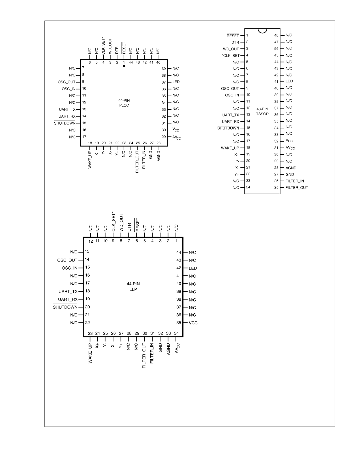
Connection Diagrams
LM8300/LM8400/LM8500
*
This pin is available in the LM8500. It is unused in the LM8300/LM8400.
20037202
Top View
Plastic Chip Package
See NS Package Number V44A
*
This pin is available in the LM8500. It is unused in the LM8300/LM8400.
20037204
Top View
TSSOP Package
See NS Package Number MTD48
*
This pin is available in the LM8500. It is unused in the LM8300/LM8400.
20037203
Top View
LLP Package
See NS Package Number LQA44A
www.national.com 4
Page 5

2.0 Pin Descriptions
Pinouts for 44- and 48-Pin Packages
Pin Name Direction Pin Description 44-Pin LLP 44-Pin PLCC 48-Pin TSSOP
RESET
DTR
WD_OUT
CLK_SET
Unused
Unused
Unused
Unused
1
2
2
2
2
OSC_OUT O Clock oscillator output 14 9 9
OSC_IN I Clock oscillator input 15 10 10
2
Unused
2
Unused
UART_TX O UART transmit pin (inverted for use
UART_RX I UART receive pin (inverted for use
SHUTDOWN I Shutdown pin, puts the device in halt
2
Unused
2
Unused
WAKE-UP I Used to wake up the processor from
X+ I/O Drives the X+ wire, also analog input
Y- I/O Drives the Y- wire, also analog input
X- I/O Drives the X- wire, also analog input
Y+ I/O Drives the Y+ wire, also analog input
2
Unused
2
Unused
FILTER_OUT O Analog output to the filter 30 25 25
FILTER_IN I Analog input from the filter 31 26 26
GND Digital ground 32 27 27
AGND Analog ground 33 28 28
AV
CC
V
CC
2
Unused
2
Unused
2
Unused
2
Unused
2
Unused
2
Unused
2
Unused
I Reset pin, pull low to reset 6 1 1
I
O
I
UART Data terminal ready signal, low
if not ready
Watchdog output, tie to RESET pin
for correct function
Used to set if crystal is 3.3 MHz (low)
or 10 MHz (floating or pulled high)
722
833
944
10 5 5
11 6 6
12 7 7
13 8 8
16 11 11
17 12 12
18 13 13
with standard RS-232 drivers)
19 14 14
with standard RS-232 drivers
20 15 15
mode if pulled low
21 16 16
22 17 17
23 18 18
halt mode with touch on touch screen
24 19 19
when sampling
25 20 20
when sampling
26 21 21
when sampling
27 22 22
when sampling
28 23 23
29 24 24
Analog power supply, connect to filter
34 29 31
for best performance
Digital power supply 35 30 32
XX33
XX34
36 31 35
37 32 36
38 33 37
39 34 38
40 35 39
LM8300/LM8400/LM8500
www.national.com5
Page 6

2.0 Pin Descriptions (Continued)
Pinouts for 44- and 48-Pin Packages (Continued)
Pin Name Direction Pin Description 44-Pin LLP 44-Pin PLCC 48-Pin TSSOP
2
Unused
LED Output Optional LED output, low when
running, high in halt-mode
2
Unused
2
Unused
LM8300/LM8400/LM8500
2
Unused
Note 1: This is available in the LM8500 only.
Note 2: These pins are for future functional expansions.
41 36 40
42 37 41
34246
44347
54448
www.national.com 6
Page 7

LM8300/LM8400/LM8500
Absolute Maximum Ratings (Note 3)
If Military/Aerospace specified devices are required,
please contact the National Semiconductor Sales Office/
Distributors for availability and specifications.
Supply Voltage (V
Voltage at Any Pin −0.3V to V
Total Current into V
)7V
CC
+0.3V
CC
Pin (Source) 200 mA
CC
Total Current out of GND Pin (Sink) 200 mA
Storage Temperature Range −65˚C to +140˚C
ESD Protection Level 2 kV (Human Body
Model)
Note 3: Absolute maximum ratings indicate limits beyond which damage to
the device may occur. DC and AC electrical specifications are not ensured
when operating the device at absolute maximum ratings.
3.0 Electrical Characteristics
TABLE 1. DC Electrical Characteristics (0˚C ≤ TA≤ +70˚C)
Datasheet min/max specification limits are guaranteed by design, test, or statistical analysis.
Parameter Conditions Min Typ Max Units
Operating Voltage 2.7 5.5 V
Power Supply Rise Time 10 50 x 10
Power Supply Ripple (Note 4) Peak-to-Peak 0.1 V
Supply Current (Note 5)
High Speed Mode
CKI = 10 MHz V
CKI = 3.33 MHz V
= 5.5V 11.5 mA
CC
= 4.5V 5 mA
CC
HALT Current with BOR Disabled (Note 6)
High Speed Mode V
Supply Current for BOR Feature V
= 5.5V, CKI=0MHz
CC
= 5.5V 45 µA
CC
<
210µA
High Brownout Trip Level (BOR Enabled) 4.17 4.28 4.5 V
Low Brownout Trip Level (BOR Enabled) 2.7 2.78 2.9 V
Input Levels (V
Logic High 0.8 V
IH,VIL
)
CC
Logic Low 0.16 V
Internal Bias Resistor for the CKI
Crystal/Resonator Oscillator
Hi-Z Input Leakage V
Input Pullup Current V
= 5.5V −0.5 +0.5 µA
CC
= 5.5V, VIN= 0V −50 −210 µA
CC
Port Input Hysteresis 0.25 V
0.3 1.0 2.5 MΩ
CC
Output Current Levels
Outputs X+, X-, Y+, Y-
Source (Note 7) V
Sink (Note 7) V
= 4.5V, VOH= 4.2V −10 mA
CC
V
= 2.7V, VOH= 2.4V −6 mA
CC
= 4.5V, VOL= 0.3V 10 mA
CC
V
= 2.7V, VOL= 0.3V 6 mA
CC
Allowable Sink and Source Current per Pin 20 mA
All Others
Source (Weak Pull-Up Mode) V
Source (Push-Pull Mode) V
Sink (Push-Pull Mode) (Note 7) V
= 4.5V, VOH= 3.8V −10 µA
CC
V
= 2.7V, VOH= 1.8V −5 µA
CC
= 4.5V, VOH= 3.8V −7 mA
CC
V
= 2.7V, VOH= 1.8V −4 mA
CC
= 4.5V, VOL= 1.0V 10 mA
CC
V
= 2.7V, VOL= 0.4V 3.5 mA
CC
Allowable Sink and Source Current per Pin 15 mA
TRI-STATE Leakage V
= 5.5V −0.5 +0.5 µA
CC
Maximum Input Current without Latchup
RAM Retention Voltage, V
(in HALT Mode) 2.0 V
R
Input Capacitance 7pF
6
CC
CC
±
200 mA
ns
V
V
V
V
www.national.com7
Page 8

Note 4: Maximum rate of voltage change must be<0.5 V/ms.
Note 5: Supply and IDLE currents are measured with CKI driven with a
square wave Oscillator, CKO driven 180˚ out of phase with CKI, inputs
connected to V
and outputs driven low but not connected to a load.
CC
Note 6: The HALT mode will stop CKI from oscillating. Measurement of I
HALT is done with device neither sourcing nor sinking current; all inputs tied
to V
; A/D converter and clock monitor and BOR disabled.
CC
Note 7: Absolute Maximum Ratings should not be exceeded.
DD
A/D Converter Electrical Characteristics (0˚C ≤ TA≤ +70˚C) (Single-ended mode only)
Datasheet min/max specification limits are guaranteed by design, test, or statistical analysis.
Parameter Conditions Min Typ Max Units
Resolution 10 Bits
DNL V
LM8300/LM8400/LM8500
DNL V
INL V
INL V
Offset Error V
Offset Error V
Gain Error V
Gain Error V
Input Voltage Range 2.7V ≤ V
CC
CC
CC
CC
CC
CC
CC
CC
=5V
=3V
=5V
=3V
=5V
=3V
=5V
=3V
<
5.5V 0 V
CC
±
1 LSB
±
1 LSB
±
2 LSB
±
4 LSB
±
1.5 LSB
±
2.5 LSB
±
1.5 LSB
±
2.5 LSB
CC
V
Analog Input Leakage Current 0.5 µA
Analog Input Resistance (Note 8) 6k Ω
Analog Input Capacitance 7pF
Operating Current on AV
Note 8: Resistance between the device input and the internal sample and hold capacitance.
CC
AVCC= 5.5V 0.2 0.6 mA
4.0 Functional Description
4.1 General
The LM8300/8400/8500 is a 4-wire resistive touch screen
controller. The primary communication is through the built in
UART operating at a baud rate of 38400. The LM8300/8400/
8500 has the ability to measure pressure on the Z-axis, in
addition to the X-Y coordinates.
The device has the capability to do a 2, 5, and 13 point
calibration. All calibration data is stored in the internal nonvolatile storage element. In addition, all settings pertaining to
the controller are stored internally. This feature negates the
need for external EEPROM.
The device has three built in averaging algorithms: oversampling, delta, and focus. These algorithms help to minimize
noise and A/D variation due to noise. Refer to the averaging
algorithm for a more detail explanation. These algorithms are
implemented on-chip, freeing the main processor from these
tasks. To further minimize noise in extremely noisy environments, the device has the ability to route the signal from the
touch panel to an external filtering stage before A/D conversions are performed.
To minimize power consumption, the device can be put into
power save mode. The device can be set to go into power
save mode automatically or manually by pulling the external
shutdown pin low.
4.2 Advanced Pin Descriptions CLK_SET — This pin is the selection pin used to determine
the operating frequency of the controller. On power up, the
controller polls this pin to determine if the operating frequency is set to 10 MHz or 3.3 MHz. If the pin is left floating
or tied high, then the operating frequency is 10 MHz. If the
pin is tied low, then the operating frequency is set to 3.3
MHz.
Note: This is available on the LM8500 only.
SHUTDOWN — This is the external shut down pin. When
pulled low, the controller goes into power saving mode. This
selection pin state has higher priority than the internal power
save mode settings.
WAKE_UP — This pin is used to wake the controller from
power save mode. When the device is in power save mode,
the pin must be tied to one of X-Y lines coming from the
touch screen panel.
X+ — Connect to X+ terminal of the resistive screen.
X- — Connect to X- terminal of the resistive screen.
Y+ — Connect to Y+ terminal of the resistive screen.
Y- — Connect to Y- terminal of the resistive screen.
Filter_out — Analog output to external filter. The use of the
external filter is controlled by sending a command byte of
$A0 on the UART to the controller.
Filter_in — Analog input from external filter. The use of the
external filter is controlled by sending a command byte of
$A0 on the UART to the controller.
LED — Optional LED output. When the controller is operating in normal (non power save) mode, a low is output to the
pin. When the controller is in power save mode, a high is
output to the pin.
RESET — Reset pin. When pulled low, a manual reset is
executed. For normal operation, this pin must be pulled high.
Under no circumstances should the pin be left floating.
Note: For the LM8400, an external reset must be used as outlined in the
Brownout Reset section.
TTL_TX — UART transmit pin. The signal is inverted for use
with standard RS-232 drivers.
TTL_RX — UART receive pin. The signal is inverted for use
with standard RS-232 drivers.
DTR — Data Terminal Ready signal for the UART. If a low
level is detected on the pin, this signals that the UART is not
ready. If a high level is detected on the pin, this signals that
the UART is ready.
www.national.com 8
Page 9

4.0 Functional Description (Continued)
WD_Out — Watch dog output. For correct operation, this
pin should be connected to the RESET pin.
OSC_OUT — Clock oscillator output pin.
OSC_IN — Clock oscillator input pin
GND — Digital Ground
AGND — Analog ground
— Digital power supply.
DV
CC
— Analog power supply. For best performance, this
AV
CC
pin should be connected to a filter.
Users of the LLP package are cautioned to be aware that the
central metal area and the pin 1 index mark on the bottom of
the package may be connected to GND. See figure below:
20037216
FIGURE 1. LLP Package Bottom View
4.3 USART Framing Format
The device communicates with the touch screen driver using
the UART set at a baud rate of 38400, 8, n, 1.
All communication from the host software and the controller
consists of a command byte and occasionally data byte(s). If
data byte(s) follow a command byte, it must be sent directly
after the command byte. If the device is in the power save
mode, a delay must be inserted between the wake up command and the command byte. Refer to the Power Save
mode section for more details. For every command byte sent
to the controller, an acknowledge byte is sent back and
sometimes data byte(s).
A command byte is distinguished by having the 7th bit of the
command byte set (1). If any data byte(s) is to follow, the 7th
bit of the data byte is reset (0).
Data packets sent to the host software can be either four or
five bytes in length. If the pressure measurement is enabled,
five bytes are sent. If the pressure measurement is not
enabled, four bytes are sent.
The first byte of each data packet is a header byte. This
header byte is used to synchronize and differentiate between
four or five byte packages. If a four byte data package is
sent, the 4th bit of the header byte is reset (0). If a five byte
data package is sent, the 4th bit of the header byte is set (1).
The 6th bit of the second byte of the data packet is used to
indicate the touch state. If the bit is set (1), then a touchdown
or continuous touch is detected. If the bit is reset (0), then a
liftoff is detected.
4.3.1. Data packet format table
Bit 7 Bit 6 Bit 5 Bit 4 Bit 3 Bit 2 Bit 1 Bit 0
Byte 1 1 0 0 L 0 0 0 0
Byte 2 0 S X
Byte 3 0 X9X8X7X6X5X4X
Byte 4 0 Y9Y8Y7Y6Y5Y4Y
Byte 5 0 Z6Z5Z4Z3Z2Z1Z
X1X0Y2Y1Y
2
0
3
3
0
L - Package length. (0 = 4 bytes,1=5bytes)
S - Touch state (0 = liftoff, 1 = touchdown or continuous
touch)
- X position (10 bit value)
X
X
- Y position (10 bit value)
Y
Y
- Z positon (7 bit value), this byte is only transmitted if the
Z
Z
pressure measurement is enabled
4.3.2 Command Bytes
PC
CommandPCByte 1PCByte 2
Read
$B0 $CA $00, $01
TSC
Byte 1
TSC
Byte 2
clock-speed
(3,33MHz,
10MHz)
Read
parameters
$B1 $CA 4.3.3
Advanced
Command
Bytes
Descriptions
Read
software
version
number
$B2 $C7 4.3.3
Advanced
Command
Bytes
Descriptions
Read # of
calibration
$B3 $CA $00, $02,
$05, $0D
points
Read stored
calibration
points
$B4 $CA 4.3.3
Advanced
Command
Bytes
Descriptions
$
Set focus
$B8 $0-$3F $CA
00-$3F
value (# of
pixels on
touch panel)
Set#of
samples per
coordinate (1,
$BA $01, $02,
$04, $08,
$10, $20
$CA $01, $02,
$04, $08,
$10, $20
2, 4, 8, 16,
32)
Set
communication
$BB $01, $02,
$04
$CA $01, $02,
$04
mode
(stream,
touchdown,
liftoff)
LM8300/LM8400/LM8500
www.national.com9
Page 10

4.0 Functional Description (Continued)
PC
CommandPCByte 1PCByte 2
Set max delta
(# of pixels
from
predicted
coordinate)
LM8300/LM8400/LM8500
Set calibration
points
Set minimum
pressure
Toggle
disable/enable
external filter
path
Toggle
disable/enable
self
power-down
Toggle
disable/enable
echo mode
Toggle
disable/enable
pressure
measurements
Toggle
disable/enable
calibration
coordinate
check
Wakeup $A7
Shutdown $A8 $CA
Soft reset $AF $CA $CB, $CC
TSC Replies
Timeout $CF
Re-send $CE
Self test failed $CC
Self test ok $CB
Acknowledge $CA
Calibration
coordinates
ok
Error / buffer
overrun
Software
version
Data transmit $80/$90 Payload
$BC $00-$3F $CA $00-$3F
$BD 4.3.3
Advanced
Command
Bytes
Descriptions
$BE $00-$7F $CA $00-$7F
$A0 $CA $00, $01
$A2 $CA $00, $01
$A3 $CA $00, $01
$A4 $CA $00, $01
$
A5 $CA $00, $01
TSC
Byte 1
$CA 4.3.3
$C4
$C8
$C7 $0-$7F
TSC
Byte 2
Advanced
Command
Bytes
Descriptions
(3/4 bytes)
4.3.3 Advanced Command Bytes Descriptions
Unless otherwise mentioned, all values are in hex.
$B0: Read clock-speed
Reply Byte #1: $CA (Acknowledge)
Byte #2: Clock readout (0 = 3.3MHz, 1 = 10MHz)
CLK_SEL pin tells the firmware which oscillator speed is
used. If the CLK_SEL input pin is floating or pulled high a
10.0MHz oscillator must be connected. If the pin is pulled
low a 3.3MHz oscillator must be connected. This command
enables the driver software to determine which oscillator
speed is used with the touch screen controller, as this determines the maximum coordinate pair per second data rates.
Note: This is available in the LM8500 only.
$B1: Read parameters
Reply Byte #1: $CA (Acknowledge)
Reply Byte #2: First byte in software version number,
year 20 (00-99)
Reply Byte #3: Communication mode (1 = stream, 2 =
touchdown, 4 = liftoff)
Byte #4: Wakeup on touch (0 = disabled, 1 = enabled)
Reply Byte #5: Number of samples (1,2, 4, 8, 16 or
32)
Byte #6: Clock readout (0 = 3.3MHz, 1 = 10MHz)
Byte #7: Second byte in software version number,
month (1-12)
Byte #8: Third byte in software version number, day
(1-31)
Byte #9: Focus value (0-63)
Byte #10: Max delta (0-63)
Byte #11: Number of calibration coordinates (0, 2, 5 or
13)
Byte #12: Toggle-flags:
Bit #5: calibration coordinates check (0=disabled,
1=enabled)
Bit #4: Pressure measurement (0=disabled,
1=enabled)
Bit #3: Echo mode (0=disabled, 1=enabled)
Bit #2: Self Power-Down mode (0=disabled,
1=enabled)
Bit #1: Unused
Bit #0: External filter path (0=disabled, 1=enabled)
Byte #13: Pressure threshold for valid touch
This command allows the user to read all the selected parameters. It is primary intended to aid in debugging. This
command can also be used if a configuration utility needs to
determine the current setting of controller.
www.national.com 10
Page 11

4.0 Functional Description (Continued)
$B2: Read software version number
Reply Byte #1: $C7 (Software version number)
Byte #2: First byte in version number, year 20 (00-99)
Byte #3: Second byte in version number, month (1-12)
Byte #4: Third byte in version number, day (1-31)
$B3: Read # of calibration points
Reply Byte #1: $CA (Acknowledge)
$
Byte #2: (
$
05 — 5 points or$0D — 13 points)
$B4: Read stored calibration points
Reply Byte #1: $CA (Acknowledge)
Byte #2: (
$
05 — 5 points or$0D — 13 points)
Byte #3: X-max (2 MSB for coordinate 1)
Byte #4: X-min (8 LSB for coordinate 1)
Byte #5: Y-max (2 MSB for coordinate 1)
Byte #6: Y-min (8 LSB for coordinate 1)
Continue until all coordinates have been sent. A zero is send
back if calibration has not been performed and there are no
data bytes.
$B8: Set focus value
Byte #2: Focus value (0-63)
Reply Byte #1: $CA (Acknowledge)
Byte #2: Focus value (0-63)
The set focus command allows the setting of different values
to improve touch screen focusing. Focusing is defined as the
ability of the touch screen controller to detect exactly identical coordinate values from measurement to measurement if
the pointer on the touch screen has not moved. The focus
values are equivalent to pixels of touch screen resolution. If
for example a value of 2 is selected, this means that every
coordinate value that is within two pixels of the previously
measured coordinate value is considered to be identical to
that previous value and that in this case the touch screen
controller transmits the previous coordinate information. This
keeps the mouse pointer steady at the point being touched,
rather than "jumping around" the point. A Focus value of zero
disables the focusing algorithm. The default setting is 4.
$BA: Set number of samples per coordinate
Byte #2: Number of samples per coordinate ($01 - 1
samples/coordinate, $02 - 2 samples/coordinate, $04
- 4 samples/coordinate, $08 - 8 samples/coordinate,
$10 - 16 samples/coordinate, $20 - 32
samples/coordinate)
Reply Byte #1: $CA (Acknowledge)
Byte #2: Number of samples per coordinate ($01 - 1
samples/coordinate, $02 - 2 samples/coordinate, $04
- 4 samples/coordinate, $08 - 8 samples/coordinate,
$10 - 16 samples/coordinate, $20 - 32
samples/coordinate)
This command allows the selection of different sample numbers per X, Y, and Z coordinates. The higher the number of
samples per X, Y, and Z coordinates, the better the accuracy,
but the lower the coordinates per second data rate. The
default setting is 8.
$BB: Set communication mode
Byte #2: Communication mode (
touchdown,
00 — no calibration done,$02 — 2 points,
$
00 — no calibration done,$02 — 2 points,
$
$
04 = liftoff)
01 = stream,$02 =
Reply Byte #1: $CA (Acknowledge)
Byte #2: Communication mode (
$
touchdown,
04 = liftoff)
$
01 = stream,$02 =
See the communication modes section for a description of
the stream, touchdown and liftoff modes. This command
selects the communication mode. The default setting is
stream mode.
$BC: Set max delta
Byte #2: Max delta value (0-63)
Reply Byte #1: $CA (Acknowledge)
Byte #2: Max delta value (0-63)
See the averaging algorithms section for a detailed description of this setting. Simply put, this command sets how much
the "coordinate velocity" can change from one coordinate to
the next. The default setting is 8.
$BD: Set calibration points
Byte #2: High nibble: Number of calibration points
$
01 = two,$02 = five,$04 = thirteen)
(
Low nibble: Active calibration cross (1-13 = cross #)
Reply Byte #1: $CA (Acknowledge)
Byte #2: High nibble: Number of calibration points
$
01=two,$02=five,$04=thirtheen)
(
Low nibble: Active calibration cross # (1-13)
Refer to the calibration section for details.
$BE: Set minimum pressure
Byte #2: Minimum pressure value (0-127)
Reply Byte #1: $CA (Acknowledge)
Byte #2: Minimum pressure value (0-127)
This setting controls how high the pressure (Z-axis) must be
in order for samples to be accepted. Setting this value too
low may result in having faulty coordinates accepted. This
value is internally multiplied by two in the controller (due to
the 7-bit limitation in the communication format, which can
not send 8-bit values larger than 127 in one byte). The
default setting is 40.
$A0: Toggle disable/enable external filter path
Reply Byte #1: $CA (Acknowledge)
Byte #2: (0 = now disabled, 1 = now enabled)
This command enable/disable external filter path. The external filter path enabled option will require the addition of a
single external low pass filter (either R/C or active OpAmp
based), which is then applied to the touch screen signal
lines. This option can be used in high noise environments to
significantly improve performance and accuracy of the touch
screen controller.
The default setting is filter path enabled.
$A2: Toggle disable/enable self-power down
Reply Byte #1: $CA (Acknowledge)
Byte #2: (0 = now disabled, 1 = now enabled)
This command can switch between self-power down mode
enable or disabled. Refer to the Power Save Mode section
for details. The default setting is Self-Power Down mode
enabled. If the echo mode is enabled, any command byte
send to the device will be echo back and executed.
$A3: Toggle disable/enable echo mode
Reply Byte #1: $CA (Acknowledge)
Byte #2: (0 = now disabled, 1 = now enabled)
The echo mode is available for debugging purposes. If enabled, the touch screen controller will echo back any data
that is received via the UART interface.
LM8300/LM8400/LM8500
www.national.com11
Page 12

4.0 Functional Description (Continued)
The default setting is Echo mode disabled.
$A4: Toggle disable/enable pressure measurement
Reply Byte #1: $CA (Acknowledge)
Byte #2: (0 = now disabled, 1 = now enabled)
The pressure measurement sets the touch screen to also
sample the Z-axis when reading the X and Y coordinates.
The default setting is pressure measurement enabled.
LM8300/LM8400/LM8500
$A7: Wakeup
There is no reply byte to this command.
When the self-power down mode of the device is enabled,
the touch screen driver must send a wakeup command prior
to any command byte(s). If the self-power down mode of the
TSC is enabled. The wakeup command must also to be sent
if the driver puts the TSC in power-down mode via the
shutdown command.
$A8: Shutdown
Reply Byte #1: $CA (Acknowledge)
When the TSC driver wants the controller to go into power
save mode it sends a shutdown command to the controller.
The driver needs to send a wakeup to the controller before
starting up the communication again.
With the TSC has the self-power-down mode enabled, then
a touchdown on the touch screen will wake-up the TSC from
shutdown mode in addition to sending the wake up command. If the self-power-down mode is disabled, then only the
wakeup command can wake-up the controller from shutdown mode (i.e. wake-up on touchdown is disabled).
$AF: Soft reset (restart the controller)
Reply Byte #1: $CA (Acknowledge)
Byte #2: $CB/$CC (Self test OK/Self test fail)
When the PC driver sends the soft reset command, the
touch screen controller executes a soft reset, which clears
and re-initializes all internal RAM configuration registers
from on-chip FLASH and performs a self-check of internal
RAM and program memory.
CONTROLLER REPLIES
$CF: Timeout.
Communication timeout has occurred, and current command
has been aborted.
$CE: Re-send
Request the TSC driver to resend the last command. This
command is used if the controller does not understand the
received command or a buffer overrun condition occurs.
$CC: Self test fail (done at startup, reset, and after
calibration)
$CB: Self test OK (done at startup, reset, and after
calibration)
$CA: Acknowledge
$C4: Calibration coordinates OK
This is sent if the coordinates are within the predefined
value.
$C8: Error / TX Buffer overrun
This is added to the last place in transmit buffer to signal that
a buffer overrun has occurred.
$C7: Software Version number
Byte #2: High part of version number (0-127)
Byte #3: Low part of version number (0-127)
$80: Format tablet for Z-axis disabled (see Format Table
section for more info.)
Byte #2: Status, low X and low Y
Byte #3: High X
Byte #4: High Y
$90: Format tablet for Z-axis enabled (see Format Table
section for more info.)
Byte #2: Status, low X and low Y
Byte #3: High X
Byte #4: High Y
Byte #5: Z-axis (0-127)
5.0 Oscillator
OSC_IN is the clock input while OSC_OUT is the clock
generator output to the crystal. Table 2 shows the compo-
nent values required for various standard crystal values.
Figure 2 shows the crystal oscillator connection diagram.
20037215
FIGURE 2. Crystal Oscillator
TABLE 2. Crystal Oscillator Configuration,
= 25˚C, VCC=5V
T
A
C1 (pF) C2 (pF)
18 18 10
18–36 18–36 3.27
The crystal and other oscillator components should be
placed in close proximity to the OSC_IN and OSC_OUT pins
to minimize printed circuit trace length.
The values for the external capacitors should be chosen to
obtain the manufacturer’s specified load capacitance for the
crystal when combined with the parasitic capacitance of the
trace, socket, and package (which can vary from 0 to 8 pF).
The guideline in choosing these capacitors is:
Manufacturer’s specified load cap = (C
C
parasitic
C2can be trimmed to obtain the desired frequency. C
should be less than or equal to C1.
CKI Freq.
(MHz)
1*C2
)/(C1+C2)+
2
www.national.com 12
Page 13

LM8300/LM8400/LM8500
6.0 Power Save Mode (Low Power Stand-by)
The power consumption of the controller can be minimized
by enabling the low power stand by mode. The power save
mode can be controlled internally by sending a command of
$A2 to the controller, externally by pulling the SHUTDOWN
pin low, or by issuing a driver shutdown command of $A8.
The self power down mode is enabled/disabled by sending a
command of $A2 to the controller. When enabled, the controller automatically goes into low power stand by if no more
touch activity is detected or if there is no UART communication. The controller automatically comes out of low power
stand by mode when a touch is detected on the touch panel
or if an incoming communication on the UART is detected. In
the low power stand by mode, all activity is disabled, including the oscillator. Also, the LED pin is driven high. To wake
up the controller on the UART, the wake up command byte
must be sent, followed by a minimum time delay of 1ms for
the LM8500 and 3ms for the LM8300/8400 before sending
any command byte. The delay time is needed to allow the
oscillator to restart and stabilize. Table 3 shows the average
startup time for a given operating frequency.
The SHUTDOWN pin will shut down the controller when
pulled low. When the SHUTDOWN pin is pulled low, the
controller will continue to be in the low power stand by mode
until the pin is pulled high or released. While the SHUTDOWN pin is pulled low, all activities are stopped and any
touch or communication will be ignored. Immediately following the SHUTDOWN pin being released or pulled high, the
controller clears the UART transmit and receive buffers and
resumes normal operation.
The controller can be put in the low power stand by mode by
sending a $A8 command to it. Upon receiving this command,
the controller goes into low power stand by mode. If the self
power down mode is enabled and the controller is put into
low power stand by mode, the controller will wake up if the
wake up command ($A7) is received or if a touch is detected
on the touch panel. If the self power down mode is disabled
and the controller is put into low power stand by mode, the
controller can only be woken up if it receives the wakeup
command. After the controller wakes up, the UART transmit
and receive buffers are cleared and resume normal operation.
Samples per coordinate vs. CPPS for LM8300/8400
Samples
per coordinate
1 250
2 220
4 190
8 150
16 100
32 65
Samples per coordinate vs. CPPS for LM8500
Samples
per coordinate
1 500
2 430
4 360
8 270
16 190
32 110
7.1 Delta Algorithm
The delta filter is used to remove large variations in sampled
values due to noise and glitches. The delta filter tries to
predict where the next coordinate could be. This is done by
taking the two previous coordinates and subtracting one
from the other, producing a delta value. This delta value is
then added or subtracted to the last coordinate. The resulting value is the predicted coordinate. If the new sampled
coordinate is close to this predicted value, then the new
value is accepted as valid and is passed to the focus algorithm, provided the focus algorithm is enabled. If the new
sampled coordinate is not close to the predicted coordinate,
then the value is discarded and is stored to be used in the
following delta calculations.
The number by which the new sampled coordinate can differ
from the predicted coordinate is controlled by setting the Set
Max Delta value. The Set Max Delta value can be from a
value of 0-63. The factory default is 8.
Coordinate pairs
per second (CPPS)
Coordinate pairs
per second (CPPS)
TABLE 3. Startup Times
CKI Frequency Startup Time
10 MHz 1–10 ms
3.33 MHz 3–10 ms
7.0 Averaging Algorithm
To achieve better accuracy and noise filtering, each X, Y, and
Z coordinate is oversampled by specific amount. The possible oversampling settings are 1, 2, 4, 8, 16, and 32. The
factory setting is 8. The greater the oversampling, the
greater the accuracy, but the lower the CPPS.
7.2 Focus Algorithm
The focus algorithm removes some inaccuracy and noise
that could cause the coordinate to differ only by a couple of
pixels. The focus algorithm is used to eliminate the "jittering"
effect of the pointer when the pointer is stationary.
The focus algorithm compares the value of the previous
stored value to the value passed from the delta algorithm
and determines if the difference is greater than or equal to
the Set Focus Value. If the difference is greater or equal to
the value in Set Focus Value then the new coordinate is sent
out through the UART and stored as the previous value. If
the difference is less than the Set Focus Value then the
value is discarded and the stored valued is set through the
UART.
The amount of difference between the new coordinate and
the old coordinate is set in the Set Focus Value. This value
can be from 0-63 with a value of 0 disabling the focus
algorithm. The factory default is 4.
www.national.com13
Page 14

7.0 Averaging Algorithm (Continued)
7.3 Communication Modes Liftoff
When set to the liftoff mode, the controller only sends data
through the UART on liftoff. The controller continuously
samples the touchscreen as long as there is a touch detected on the touchscreen but only the last coordinate is sent
out to the UART.
Touchdown
LM8300/LM8400/LM8500
When set to the touchdown mode, the controller only sends
data through the UART on touchdown. The controller continuously samples the touchscreen as long as there is a
touch detected on the touchscreen but only the first coordinate is sent out to the UART.
Streaming
When set to the streaming mode, the controller continuously
sends data through the UART as long as there is a touch
detected on the touchscreen.
8.0 Brownout Reset
The device is initialized when the RESET pin is pulled low or
the On-chip Brownout Reset is activated. The Brownout
Reset feature is not available on the LM8400.
The RESET input initializes the device when pulled low. The
RESET pin must be held low for a minimum of 0.5µs for the
LM8500 and a minimum of 1.5µs for the LM8300/8400 to
guarantee a valid reset. During Power-Up initialization, the
user must ensure that the RESET pin of a device without the
Brownout Reset feature is held low until the device is within
the specified V
with a delay 5 times (5x) greater than the power supply rise
time is recommended. Reset should also be wide enough to
ensure crystal start-up upon power-up. A recommended reset circuit for this device is shown in Figure 3.
voltage. An R/C circuit on the RESET pin
CC
20037205
FIGURE 3. Reset Circuit using External Reset
When enabled, the device generates an internal reset as
V
rises. While VCCis less than the specified brownout
CC
voltage (V
), the device is held in the reset condition for t
bor
= 120-128 µs for the LM8500 and tid= 360-384 µs for the
LM8300. Once the t
reaches zero, the internal reset is
id
released and the controller resume normal operation. This
internal reset will perform the same functions as external
reset. Once V
is above the V
CC
instruction execution begins. If, however, V
the selected V
, an internal reset is generated, and tidis set
bor
and tidreaches zero,
bor
drops below
CC
to 120-128 µs for the LM8500 and 360-384 µs for the
LM8300. The device now waits until V
is greater than V
CC
bor
at which time the countdown starts over. When enabled, the
functional operation of the device, at frequency, is guaranteed down to the V
level.
bor
One exception to the above is that the brownout circuit will
insert a delay of approximately 3 ms on power up or any time
the V
be held in Reset for the duration of this delay before t
count down. This delay starts as soon as the V
drops below a voltage of about 1.8V. The device will
CC
CC
id
starts
rises
above the trigger voltage (approximately 1.8V). This behavior is shown in Figure 4.
In Case 1, V
rises from 0V and the on-chip RESET is
CC
undefined until the supply is greater than approximately
1.0V. At this time the brownout circuit becomes active and
holds the device in RESET. As the supply passes a level of
about 1.8V, a delay of about 3 ms (td) is started and t
id
preset with 120-128 µs for the LM8500 or 360-384 µs for the
LM8300. Once V
starts to count down.
t
id
is greater than V
CC
and td has expired,
bor
Case 2 shows a subsequent dip in the supply voltage which
goes below the approximate 1.8V level. As V
, the internal RESET signal is asserted. When VCCrises
V
bor
drops below
CC
back above the 1.8V level, td is started. Since the power
supply rise time is longer for this case, td has expired before
rises above V
V
CC
greater than V
Case 3 shows a dip in the supply where V
, but not below 1.8V. On-chip RESET is asserted when
V
bor
goes below V
V
CC
goes back above V
and tidstarts immediately when VCCis
bor
.
bor
and tidstarts as soon as the supply
bor
.
bor
drops below
CC
id
,
is
www.national.com 14
Page 15

8.0 Brownout Reset (Continued)
LM8300/LM8400/LM8500
FIGURE 4. Brownout Reset Operation
If the Brownout Reset feature is enabled, the internal reset
will not be turned off until t
counts down to zero. The
id
internal reset will perform the same functions as external
reset. The device is guaranteed to operate at the specified
frequency down to the specified brownout voltage. After the
underflow, the logic is designed such that no additional
internal resets occur as long as V
remains above the
CC
brownout voltage.
The device is relatively immune to short duration negative
going V
transients (glitches). Proper filtering of the V
CC
CC
power supply voltage is essential for proper brownout functionality. Power supply decoupling is vital even in battery
powered systems.
There are two optional brownout voltages. The part numbers
for the three versions of this device are:
LM8500, V
LM8300, V
= high voltage range.
bor
= low voltage range.
bor
LM8400, BOR is disabled.
Refer to the device specifications for the actual V
volt-
bor
ages.
High brownout voltage devices are guaranteed to operate at
10MHz down to the high brownout voltage. Low brownout
voltage devices are guaranteed to operate at 3.33MHz down
to the low brownout voltage. Low brownout voltage devices
are not guaranteed to operate at 10MHz down to the low
brownout voltage.
Under no circumstances should the RESET pin be allowed
to float. If the on chip Brownout Reset feature is being used,
the RESET pin should be connected directly to V
CC
. The
20037206
RESET input may also be connected to an external pull-up
resistor or to other external circuitry. The output of the brownout reset detector will always preset t
to a value between
id
120-128µs for the LM8500 and 360-384µs for the LM8300.
At this time, the internal reset will be generated.
If the BOR feature is disabled, then no internal resets are
generated. In this case, the external RESET must be used.
When BOR is disabled, this on-chip circuitry is disabled and
draws no DC current.
9.0 Calibration
The device supports two, five, and thirteen point calibration.
If desired, the calibration points can be stored internally in
the non-volatile storage element. During calibration time, the
device has the unique ability to check if the calibration points
make sense. For instance, if the desired calibration point
was to be at the upper left hand corner, but by accident, the
actual point detected was at the lower right hand corner, the
device will reject this point. This ensures the calibration
process is not performed incorrectly.
The calibration checking, can be enabled or disabled. If the
calibration checking is enabled, the controller will always
check the current calibration point being done against the
theoretical point and determine if the value is within
the raw A/D values. If this option is desired, the touch screen
driver must perform the calibration according to the calibration mapping for the two, five, and thirteen points as shown
in Figure 5, Figure 6, and Figure 7, respectively. The theoretical values for the two, five, and thirteen points are shown
in Table 4, Table 5, and Table 6 respectively.
±
127 of
www.national.com15
Page 16

9.0 Calibration (Continued)
LM8300/LM8400/LM8500
TABLE 4. Two Points Calibration
Calibration point Theoretical X-value Theoretical Y-value
1 127 127
2 895 895
TABLE 5. Five Points Calibration
Calibration point Theoretical X-value Theoretical Y-value
1 127 127
2 895 895
3 127 895
4 511 511
5 895 127
FIGURE 5. Two Points Calibration Mapping
FIGURE 6. Five Points Calibration Mapping
20037207
20037208
TABLE 6. Thirteen Points Calibration
Calibration point Theoretical X-value Theoretical Y-value
1 127 127
2 895 895
3 127 895
4 511 511
5 895 127
6 895 511
7 511 895
8 127 511
9 511 127
10 623 319
11 623 623
12 319 623
13 319 319
20037209
FIGURE 7. Thirteen Points Calibration Mapping
www.national.com 16
Page 17

9.0 Calibration (Continued)
9.1 General Calibration Procedures
Calibration is invoked by sending a command byte of $BD
followed by a command byte to the device. The command
byte is broken into two parts: the high nibble states the
number of calibration points to performs and the lower nibble
states the active calibration point. For example, to do the first
calibration point for the two point calibration, the command
bytes of $BD and $11 are sent to the device. The device then
echos $BD and $11 back to the TS driver and waits for a
touch on the panel. When a touch is detected, the device
checks to see if the point is within the specified parameters
if the calibration point checking is enabled. If the calibration
point checking is disabled, the device will send a
byte to the TS driver regardless of where the touch was
detected. This calibration point checking can be enabled or
disabled by sending a command byte of $A5 to the device.
When all the calibration points are done, the device will do a
self-test and send a command of $CB for OK or a command
of $CC for failed. If a $CC is received, the TS driver should
issue a warning stating the calibration was not done properly
and redo the calibration procedures. The flowchart for the
calibration procedures is shown in Figure 8.
$
C8 for OK
LM8300/LM8400/LM8500
FIGURE 8. Calibration Procedures with Coordinates Checking Enabled
20037210
www.national.com17
Page 18

9.0 Calibration (Continued)
9.2 Calibration Procedures with Coordinates Checking Enabled
To do TS calibration with coordinates checking enabled, first
ensure the Calibration Coordinates Checking is enabled on
the device. This can be accomplished by sending a command byte of $B1 (Read Parameters command) and checking the 5th bit of the 12th reply byte is set. Alternatively, if the
device is set to Calibration Coordinates Checking enabled
LM8300/LM8400/LM8500
as default, this step can be skipped.
The TS driver sends the command byte to do calibration
($BD). The TS driver should wait for the reply bytes and
ensure it is the same command bytes it sent. The device
waits for a touch to be detected on the panel. Once a touch
is detected, the device checks it against the predetermined
calibration values as noted on Table 4, Table 5 , and Table 6.
If the detected touch is within the predefined value (
the raw A/D value), the device will send a command of $C4
to the TS driver and store the calibration point in the internal
flash. The TS driver can now send a command byte to do the
next calibration point. If the detected touch is not within the
predefined value, the device will send a reply byte of $C8 to
the TS driver. Upon receiving this reply byte, the TS driver
can resend the calibration command for the same calibration
point, go the next calibration point, or abort the calibration
process.
Once all the calibration points are done, the device does a
self-test. If the self-test was not successful, the device will
send a reply byte of $CC to the TS driver. At this point, the
TS driver should either notify the user to redo the calibration
±
127 of
point or automatically redo the calibration again. If the selftest was successful, the device will send a reply byte of $CB
to the TS driver.
9.3 Calibration Procedures with Coordinates Checking Disabled
To do TS calibration with coordinates checking disabled, first
ensure the Calibration Coordinates Checking is disabled on
the device. This can be accomplished by sending a command byte of $B1 (Read Parameters command) and checking the 5th bit of the 12th reply byte is not set. Alternatively,
if the device is set to Calibration Coordinates Checking
disabled as default, this step can be skipped.
The TS driver sends the command byte to do calibration
($BD). The TS driver should wait for the reply bytes and
ensure it is the same command bytes it sent. The device
waits for a touch to be detected on the panel. Once a touch
is detected, the device save the values into the internal flash
and send a reply byte of $C4 to the TS driver. The TS driver
can now send a command byte to do the next calibration
point. Since the Calibration Checking is disabled, the TS
driver should ensure the calibration point is within the range
of the calibration cross.
Once all the calibration points are done, the device does a
self-test. If the self-test was not successful, the device will
send a reply byte of $CC to the TS driver. At this point, the
TS driver should either notify the user to redo the calibration
point or automatically redo the calibration again. If the selftest was successful, the device will send a reply byte of $CB
to the TS driver.
www.national.com 18
Page 19

Physical Dimensions inches (millimeters) unless otherwise noted
LM8300/LM8400/LM8500
LLP Package (LQA)
Order Number LM8300HLQ9 or LM8400HLQ9 or LM8500HLQ9
NS Package Number LQA44A
TSSOP Package (MTD)
Order Number LM8300IMT9 or LM8400IMT9 or LM85009IMT9
NS Package Number MTD48
www.national.com19
Page 20

Physical Dimensions inches (millimeters) unless otherwise noted (Continued)
Plastic Leaded Chip Carrier (VA)
Order Number LM8300HVA9 or LM8400HVA9 or LM8500HVA9
NS Package Number V44A
LIFE SUPPORT POLICY
NATIONAL’S PRODUCTS ARE NOT AUTHORIZED FOR USE AS CRITICAL COMPONENTS IN LIFE SUPPORT
DEVICES OR SYSTEMS WITHOUT THE EXPRESS WRITTEN APPROVAL OF THE PRESIDENT AND GENERAL
COUNSEL OF NATIONAL SEMICONDUCTOR CORPORATION. As used herein:
1. Life support devices or systems are devices or
systems which, (a) are intended for surgical implant
into the body, or (b) support or sustain life, and
whose failure to perform when properly used in
LM8300/LM8400/LM8500 Four Wire Resistive Touchscreen Controller with Brownout
accordance with instructions for use provided in the
2. A critical component is any component of a life
support device or system whose failure to perform
can be reasonably expected to cause the failure of
the life support device or system, or to affect its
safety or effectiveness.
labeling, can be reasonably expected to result in a
significant injury to the user.
National Semiconductor
Americas Customer
Support Center
Email: new.feedback@nsc.com
Tel: 1-800-272-9959
www.national.com
National does not assume any responsibility for use of any circuitry described, no circuit patent licenses are implied and National reserves the right at any time without notice to change said circuitry and specifications.
National Semiconductor
Europe Customer Support Center
Fax: +49 (0) 180-530 85 86
Email: europe.support@nsc.com
Deutsch Tel: +49 (0) 69 9508 6208
English Tel: +44 (0) 870 24 0 2171
Français Tel: +33 (0) 1 41 91 8790
National Semiconductor
Asia Pacific Customer
Support Center
Fax: 65-6250 4466
Email: ap.support@nsc.com
Tel: 65-6254 4466
National Semiconductor
Japan Customer Support Center
Fax: 81-3-5639-7507
Email: nsj.crc@jksmtp.nsc.com
Tel: 81-3-5639-7560
 Loading...