

Datasheet LM8365BCLMFX30, LM8365BALMFX45, LM8365BALMFX22, LM8365BALMF45, LM8365BALMF22 Datasheet (NSC)
...Page 1
LM8365
Micropower Undervoltage Sensing Circuits with
Programmable Output Delay
LM8365 Micropower Undervoltage Sensing Circuits with Programmable Output Delay
March 2003
General Description
The LM8365 series are micropower undervoltage sensing
circuits that are ideal for use in battery powered microprocessor based systems, where extended battery life is a key
requirement.
A range of threshold voltages from 2.0V to 4.5V are available
with an active low, open drain or CMOS, output. These
devices feature a very low quiescent current of 0.65µA typical. The LM8365 series features a highly accurate voltage
reference, a comparator with precise thresholds and built-in
hysterisis to prevent erratic reset operation, a time delayed
output which can be programmed by the system designer,
and guaranteed Reset operation down to 1.0V with extremely low standby current.
These devices are available in the space saving 5-Pin
SOT23 surface mount package. For additional undervoltage
thresholds and output options, please contact National
Semiconductor.
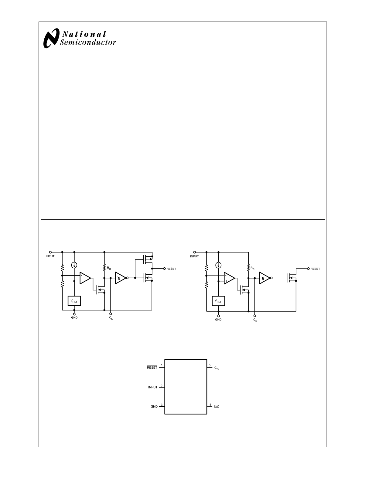
Functional Diagrams
CMOS Output Open Drain Output
Features
n Extremely Low Quiescent Current: 0.65µA, at VIN=
2.87V
n High Accuracy Threshold Voltage (
n Complementary or Open Drain Output
n Programmable output delay by external Capacitor
(100ms typ with 0.1µF)
n Input Voltage Range: 1V to 6V
n Surface Mount Package (5-Pin SOT23)
n Pin for pin compatible with MC33465
±
2.5%)
Applications
n Low Battery Detection
n Microprocessor Reset Controller
n Power Fail Indicator
n Battery Backup Detection
20066013
20066014
Connection Diagram
5-Pin SOT23
Top View
© 2003 National Semiconductor Corporation DS200660 www.national.com
20066012
Page 2
Pin Description
LM8365
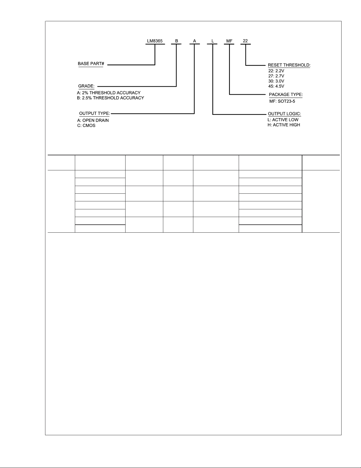
Ordering Information
20066015
Package Part Number Package
Marking
5-Pin
SOT23
LM8365BALMF22
LM8365BALMFX22 3k Units Tape and Reel
LM8365BALMF27
LM8365BALMFX27 3k Units Tape and Reel
LM8365BCLMF30
LM8365BCLMFX30 3k Units Tape and Reel
LM8365BALMF45
LM8365BALMFX45 3k Units Tape and Reel
F08A 2.2V
F07A 2.7V
F02A 3.0V
F06A 4.5V
Threshold Output Type Transport Media NSC Drawing
Open Drain,
Active Low
Open Drain,
Active Low
CMOS, Active
Low
Open Drain,
Active Low
1k Units Tape and Reel
1k Units Tape and Reel
1k Units Tape and Reel
1k Units Tape and Reel
MF05A
www.national.com 2
Page 3
LM8365
Absolute Maximum Ratings (Note 1)
Junction Temperature 125˚C
If Military/Aerospace specified devices are required,
please contact the National Semiconductor Sales Office/
Distributors for availability and specifications.
Supply Voltage −0.3V to 6.5V
RESET Output Voltage
RESET Output Current
−0.3V to 6.5V
70mA
Storage Temperature Range −65˚C to 150˚C
Mounting Temperature
Operating Ratings (Note 1)
Temperature Range −40˚C to 85˚C
Thermal Resistance to Ambient (θ
ESD Tolerance
Human Body Model 2000V
Machine Model 200V
) 265˚C/W
JA
Lead Temp. (Soldering 10 sec) 260˚C
Electrical Characteristics
Unless otherwise specified, all limits guaranteed for TA= 25˚C.
Symbol Parameter Conditions Min
(Note 3)
High to Low State Output
Decreasing)
(V
IN
V
DET−
Detector Threshold Voltage
22 Suffix 2.145 2.2 2.255
27 Suffix 2.633 2.7 2.767
30 Suffix 2.925 3.0 3.075
45 Suffix 4.388 4.5 4.613
V
Increasing
IN
22 Suffix 0.066 0.110 0.154
V
HYS
Detector Threshold Hysteresis
27 Suffix 0.081 0.135 0.189
30 Suffix 0.090 0.150 0.210
45 Suffix 0.135 0.225 0.315
∆Vdet/∆T Detector Threshold Voltage
Temperature Coefficient
V
OH
V
OL
I
OL
I
OH
I
CD
R
D
V
IN
RESET Output Voltage (CMOS Output: I
SOURCE
= 1mA)
-2.1 VIN-1.0
V
IN
(Open Drain or CMOS Output:
= 1mA)
I
SINK
RESET Output Sink Current VIN= 1.5V, VOL= 0.5V 1.0 2.5 mA
RESET Output Source Current VIN= 4.5V, VOL= 2.4V 1.0 7.0 mA
Delay Pin Output Sink Current VIN= 1.5V, VCD= 0.5V 0.2 1.8 mA
Delay Resistance 0.5 1.0 2.0 MΩ
Operating Input Voltage Range 1.0 6.0 V
22 Suffix
= 2.10V 0.57 0.8
V
IN
V
= 4.20V 0.71 1.3
IN
27 Suffix
V
= 2.60V 0.62 0.9
IN
V
= 4.70V 0.75 1.3
I
IN
Quiescent Input Current
IN
30 Suffix
V
= 2.87V 0.65 0.9
IN
V
= 5.00V 0.77 1.3
IN
45 Suffix
V
= 4.34V 0.70 1.0
IN
V
= 6.00V 0.85 1.4
IN
Note 1: Absolute Maximum Ratings indicate limits beyond which damage to the device may occur. Operating Ratings indicate conditions for which the device is
intended to be functional, but specific performance is not guaranteed. For guaranteed specifications and the test conditions, see the Electrical Characteristics.
Note 2: Typical values represent the most likely parametric norm.
Note 3: All limits are guaranteed by testing or statistical analysis.
Typ
(Note 2)
±
100 PPM/˚C
0.25
Max
(Note 3)
V
IN
0.5 V
Units
V
V
µA
www.national.com3
Page 4

Typical Performance Characteristics
LM8365
Input Current vs. Input Voltage
LM8365BALMF45
Reset Output Sink Current vs. Input Voltage
LM8365BALMF27
Reset Output Voltage vs. Input Voltage
LM8365BALMF45
20066001 20066002
Reset Output Source Current vs. Input Voltage
LM8365BCLMF30
20066003 20066004
Reset Output Sink Current vs. Reset Output Voltage
LM8365BALMF45
20066005
www.national.com 4
C
Sink Current vs. Input Voltage
D
LM8365BALMF27
20066006
Page 5

Typical Performance Characteristics (Continued)
C
C
Sink Current vs. CDVoltage
D
D
LM8365
Delay Pin Threshold Voltage vs. Temperature
LM8365BALMF27
20066007
Detector Threshold Voltage vs. Temperature
LM8365BALMF45 Delay Resistance vs. Temperature
20066009
Output Time Delay vs. Capacitance
20066008
20066010
20066011
www.national.com5
Page 6

Application Notes
The propagation delay time for the LM8365 is measured
LM8365
using a 470kΩ pull-up resistor connected to from the RESET
output pin to 5V in addition to a 10pF capacitive load connected from the same pin to GND. Figure 1 shows the timing
diagram for the measurement for the propagation delay.
is equal to the sum of the detector threshold, V
V
DET+
and the built in hysteresis, V
from High-to-Low and t
HYS.tD1
D2
is the propagation time
is the propagation from
DET−
Low-to-High.
,
FIGURE 1. Propagation Delay Timing Diagrams
The LM8365 ultra-low current voltage detector was designed
to monitor voltages and to provide an indication when the
monitored voltage, V
, dropped below a precisely trimmed
IN
threshold voltage. The voltage detector of the LM8365 drives
a time delay generator that may be programmed for fixed
lengths of time depending on the application needs. This
characteristic is displayed in the typical operating timing
diagram in Figure 2.V
is the voltage that is being moni-
IN
tored and as it decreases passed the precisely trimmed
threshold V
the Active Low RESET output drops to a
DET−
Logic Low state and the CDpin drops to 0V. During this state
the external capacitor connected to the C
pin is immedi-
D
ately discharged by an internal N-Channel MOSFET. When
increases above the threshold V
V
IN
capacitor connected to the C
DET+(VDET−+VHYS
pin starts to charge up to V
D
) the
20066016
through an internal pull-up resistor RD. Once the capacitor
has charged up past the internal Delay Pin Threshold, which
is typically 0.675 V
, the RESET output will revert back to
IN
it’s original state. The LM8365 has built-in hysteresis to help
prevent erratic reset operation when the input voltage
crosses the threshold.
The LM8365 has a wide variety of applications that can take
advantage of it’s precision and low current consumption to
monitor Input voltages even though it was designed as a
reset controller in portable microprocessor based systems. It
is a very cost effective and space saving device that will
protect your more expensive investments of microprocessors and other devices that need a guaranteed supply voltage and time delay for proper operation.
IN
www.national.com 6
Page 7

Application Notes (Continued)
LM8365
FIGURE 2. Timing Waveforms
20066017
www.national.com7
Page 8

Typical Applications
LM8365
Microprocessor Reset Circuit
Battery Charge Indicator Using LM8365BCLMF30
20066018
20066019
Missing Pulse Detector or Frequency Detector Using LM8365BALMF45
www.national.com 8
20066020
Page 9

Physical Dimensions inches (millimeters)
unless otherwise noted
LM8365 Micropower Undervoltage Sensing Circuits with Programmable Output Delay
5-Pin SOT23-5
NSC Package Number MF05A
LIFE SUPPORT POLICY
NATIONAL’S PRODUCTS ARE NOT AUTHORIZED FOR USE AS CRITICAL COMPONENTS IN LIFE SUPPORT
DEVICES OR SYSTEMS WITHOUT THE EXPRESS WRITTEN APPROVAL OF THE PRESIDENT AND GENERAL
COUNSEL OF NATIONAL SEMICONDUCTOR CORPORATION. As used herein:
1. Life support devices or systems are devices or
systems which, (a) are intended for surgical implant
into the body, or (b) support or sustain life, and
whose failure to perform when properly used in
accordance with instructions for use provided in the
2. A critical component is any component of a life
support device or system whose failure to perform
can be reasonably expected to cause the failure of
the life support device or system, or to affect its
safety or effectiveness.
labeling, can be reasonably expected to result in a
significant injury to the user.
National Semiconductor
Americas Customer
Support Center
Email: new.feedback@nsc.com
Tel: 1-800-272-9959
www.national.com
National Semiconductor
Europe Customer Support Center
Fax: +49 (0) 180-530 85 86
Email: europe.support@nsc.com
Deutsch Tel: +49 (0) 69 9508 6208
English Tel: +44 (0) 870 24 0 2171
Français Tel: +33 (0) 1 41 91 8790
National Semiconductor
Asia Pacific Customer
Support Center
Fax: +65-6250 4466
Email: ap.support@nsc.com
Tel: +65-6254 4466
National Semiconductor
Japan Customer Support Center
Fax: 81-3-5639-7507
Email: jpn.feedback@nsc.com
Tel: 81-3-5639-7560
National does not assume any responsibility for use of any circuitry described, no circuit patent licenses are implied and National reserves the right at any time without notice to change said circuitry and specifications.
 Loading...