

Page 1
LM833
Dual Audio Operational Amplifier
LM833 Dual Audio Operational Amplifier
August 1997
General Description
The LM833 is a dual general purpose operational amplifier
designed with particular emphasis on performance in audio
systems.
This dual amplifier IC utilizes new circuit and processing
techniques to deliver low noise, high speed and wide bandwidth without increasing external components or decreasing
stability. The LM833 is internally compensated for all closed
loop gains and is thereforeoptimizedforallpreampand high
level stages in PCM and HiFi systems.
The LM833 is pin-for-pin compatible with industry standard
dual operational amplifiers.
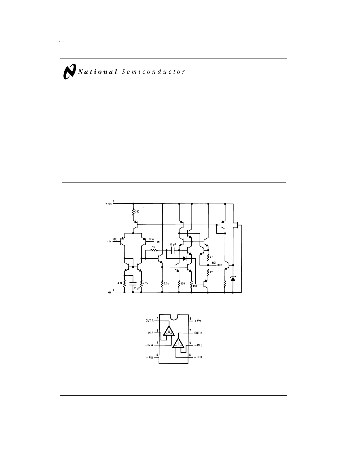
Schematic Diagram (1/2 LM833)
Features
n Wide dynamic range: 140dB
n Low input noise
voltage: 4.5nV/
n High slew rate: 7 V/µs (typ); 5V/µs (min)
n High gain bandwidth: 15MHz (typ); 10MHz (min)
n Wide power bandwidth: 120KHz
n Low distortion: 0.002
n Low offset voltage: 0.3mV
n Large phase margin: 60˚
n Available in 8 pin MSOP package
√
Hz
%
DS005218-1
Connection Diagram
DS005218-2
Order Number LM833M, LM833N or LM833MM
© 1999 National Semiconductor Corporation DS005218 www.national.com
See NS Package Number
M08A, N08E or MUA08A
Page 2
Absolute Maximum Ratings (Note 1)
If Military/Aerospace specified devices are required,
please contact the National Semiconductor Sales Office/
Distributors for availability and specifications.
Supply Voltage V
CC–VEE
Differential Input Voltage (Note 3) V
Input Voltage Range (Note 3) V
Power Dissipation (Note 4) P
Operating Temperature Range T
Storage Temperature Range T
IC
D
OPR
STG
I
36V
±
30V
±
15V
500 mW
−40z85˚C
−60z150˚C
Soldering Information
Dual-In-Line Package
Soldering (10 seconds) 260˚C
Small Outline Package
(SOIC and MSOP)
Vapor Phase (60 seconds) 215˚C
Infrared (15 seconds) 220˚C
See AN-450 “Surface Mounting Methods and Their Effect
on Product Reliability” for other methods of soldering
surface mount devices.
ESD tolerance (Note 5) 1600V
DC Electrical Characteristics (Notes 1, 2)
=
(T
25˚C, V
A
Symbol Parameter Conditions Min Typ Max Units
V
OS
I
OS
I
B
A
V
V
OM
V
CM
CMRR Common-Mode Rejection Ratio V
PSRR Power Supply Rejection Ratio V
I
Q
=
±
15V)
S
Input Offset Voltage R
=
10Ω 0.3 5 mV
S
Input Offset Current 10 200 nA
Input Bias Current 500 1000 nA
Voltage Gain R
Output Voltage Swing R
Input Common-Mode Range
Supply Current V
=
2kΩ,V
L
=
10 kΩ
L
=
R
2kΩ
L
=
IN
=
15
S
=
0V, Both Amps 5 8 mA
O
=
±
10V 90 110 dB
O
±
12V 80 100 dB
z
5V, −15z−5V 80 100 dB
±
12
±
10
±
12
±
13.5 V
±
13.4 V
±
14.0 V
AC Electrical Characteristics
=
(T
25˚C, V
A
Symbol Parameter Conditions Min Typ Max Units
SR Slew Rate R
GBW Gain Bandwidth Product f=100 kHz 10 15 MHz
=
±
S
15V, R
=
2kΩ)
L
=
2kΩ 5 7 V/µs
L
Design Electrical Characteristics
=
(T
25˚C, V
A
The following parameters are not tested or guaranteed.
Symbol Parameter Conditions Typ Units
/∆T Average Temperature Coefficient 2 µV/˚C
∆V
OS
THD Distortion R
e
n
i
n
PBW Power Bandwidth V
f
U
φ
M
www.national.com 2
=
±
15V)
S
of Input Offset Voltage
Input Referred Noise Voltage R
=
2kΩ,f=20
L
=
V
3 Vrms, A
OUT
=
100Ω,f=1 kHz 4.5
S
z
20 kHz 0.002
=
1
V
Input Referred Noise Current f=1 kHz 0.7
=
27 V
O
pp,RL
=
2kΩ, THD ≤ 1
%
120 kHz
Unity Gain Frequency Open Loop 9 MHz
Phase Margin Open Loop 60 deg
Input Referred Cross Talk f=20
z
20 kHz −120 dB
%
Page 3
Design Electrical Characteristics (Continued)
Note 1:
Absolute Maximum Ratings
tional, but do not guarantee specific performance limits.
antee specific performance limits. This assumes that the device is within the Operating Ratings. Specifications are not guaranteed for parameters where no limit is
given, however, the typical value is a good indication of device performance.
Note 2: All voltages are measured with respect to the ground pin, unless otherwise specified.
Note 3: If supply voltage is less than
Note 4: This is the permissible value at T
Note 5: Human body model, 1.5 kΩ in series with 100 pF.
indicate limits beyond which damage to the device may occur.
±
15V, it is equal to supply voltage.
A
Electrical Characteristics
≤ 85˚C.
state DC and AC electrical specifications under particular test conditions which guar-
Operating Ratings
indicate conditions for which the device is func-
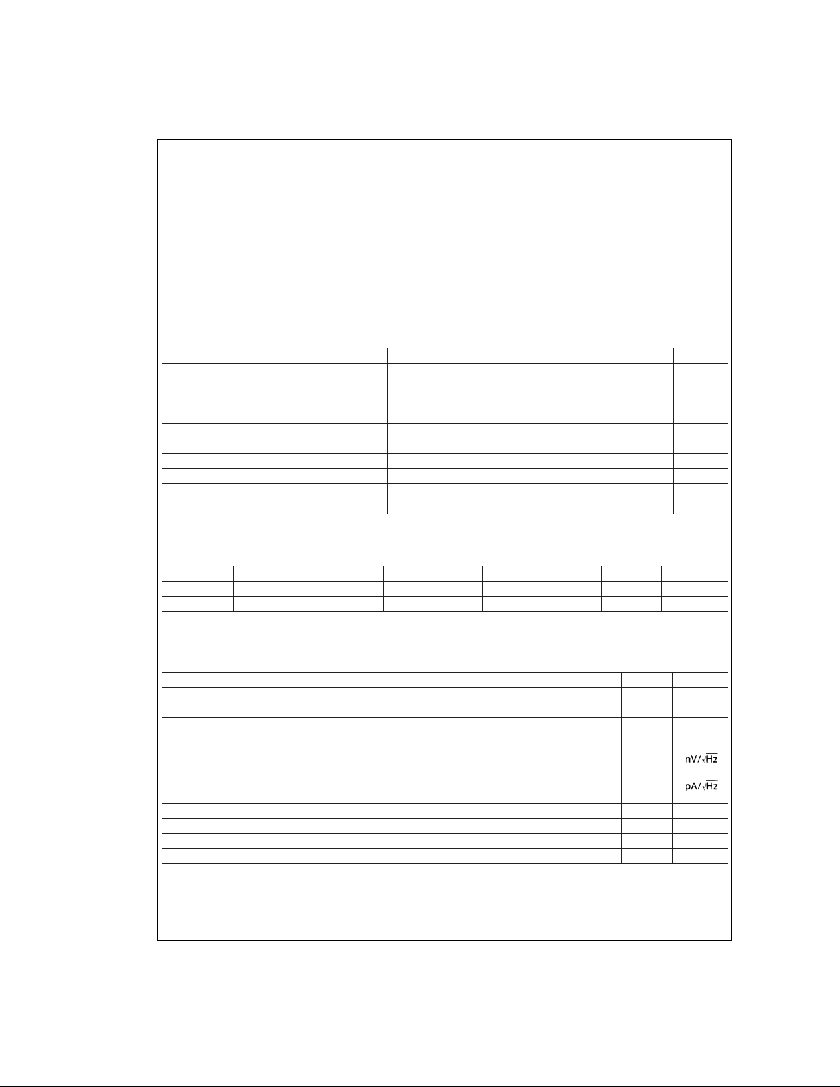
Typical Performance Characteristics
Maximum Power
Dissipation
vs Ambient Temperature
Supply Current vs
Supply Voltage
DS005218-4
DS005218-7
Input Bias Current vs
Ambient Temperature
DC Voltage Gain
vs Ambient Temperature
DS005218-5
DS005218-8
Input Bias Current vs
Supply Voltage
DS005218-6
DC Voltage Gain
vs Supply Voltage
DS005218-9
Voltage Gain & Phase
vs Frequency
DS005218-10
Gain Bandwidth Product
vs Ambient Temperature
DS005218-11
Gain Bandwidth
vs Supply Voltage
DS005218-12
www.national.com3
Page 4
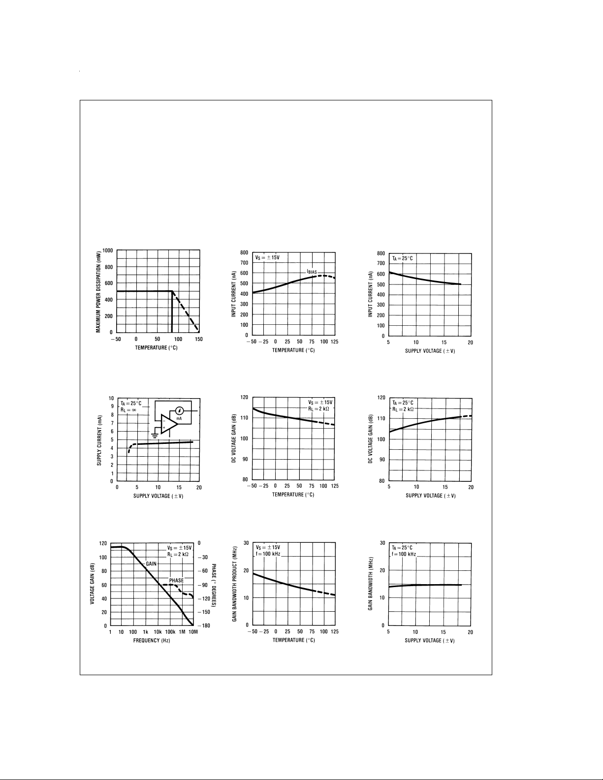
Typical Performance Characteristics (Continued)
Slew Rate vs
Ambient Temperature
CMR vs Frequency
Maximum
Output Voltage vs
Supply Voltage
DS005218-13
DS005218-19
Slew Rate vs
Supply Voltage
Distortion vs Frequency
Maximum
Output Voltage vs
Ambient Temperature
DS005218-14
DS005218-20
Power Bandwidth
DS005218-15
PSRR vs Frequency
DS005218-18
DS005218-16
www.national.com 4
DS005218-17
Page 5
Typical Performance Characteristics (Continued)
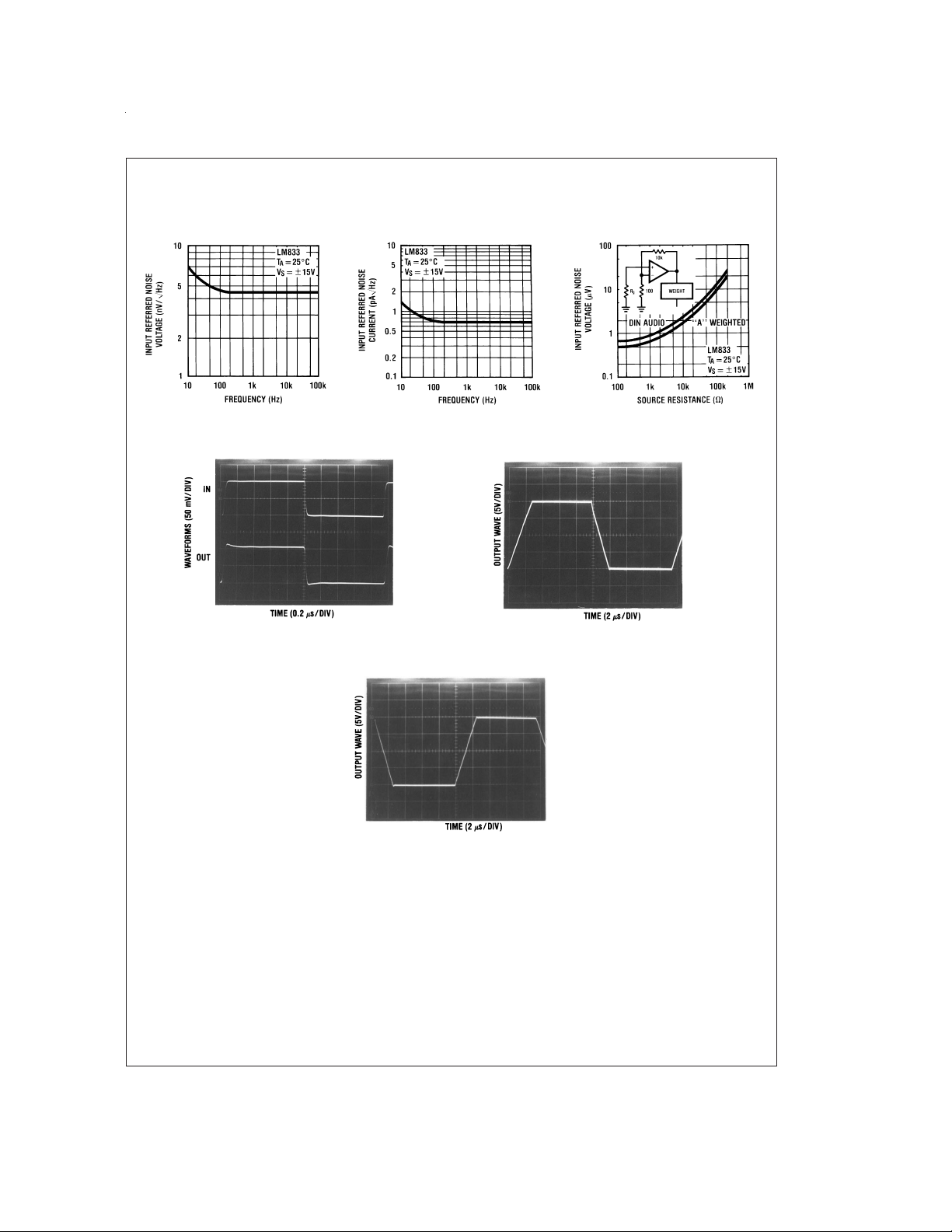
Spot Noise Voltage
vs Frequency
Noninverting Amp
Inverting Amp
DS005218-21
Spot Noise Current
vs Frequency
DS005218-24
DS005218-22
Noninverting Amp
Input Referred Noise Voltage
vs Source Resistance
DS005218-23
DS005218-25
Application Hints
The LM833 is a high speed op amp with excellent phase
margin and stability. Capacitive loads up to 50 pF will cause
little change in the phase characteristics of the amplifiers
and are therefore allowable.
DS005218-26
Capacitive loads greater than 50 pF must be isolated from
the output. The most straightforward way to do this is to put
a resistor in series with the output. This resistor will also prevent excess power dissipation if the output is accidentally
shorted.
www.national.com5
Page 6

Noise Measurement Circuit
Complete shielding is required to prevent induced pick up from external sources. Always check with oscilloscope for power line noise.
RIAA Preamp Voltage Gain, RIAA
Deviation vs Frequency
Input Referred Noise Voltage: e
Total Gain: 115 dB@f=1 kHz
Flat Amp Voltage Gain vs
Frequency
DS005218-28
=
V0/560,000 (V)
n
DS005218-29
DS005218-27
www.national.com 6
Page 7

Typical Applications
NAB Preamp
Adder/Subtracter
=
A
34.5
V
F=1 kHz
=
0.38 µV
E
n
A Weighted
DS005218-30
NAB Preamp Voltage Gain
vs Frequency
DS005218-31
Balanced to Single Ended Converter
=
V
V1+V2−V3−V4
O
DS005218-33
Sine Wave Oscillator
DS005218-34
=
V
V1–V2
O
DS005218-32
www.national.com7
Page 8

Typical Applications (Continued)
Second Order High Pass Filter
(Butterworth)
DS005218-35
Illustration is f
Illustration is f
=
1 kHz
0
Second Order Low Pass Filter
(Butterworth)
DS005218-36
=
1 kHz
0
www.national.com 8
Page 9

Typical Applications (Continued)
State Variable Filter
DS005218-37
Illustration is f
=
1 kHz, Q=10, A
0
=
1
BP
2 Channel Panning Circuit (Pan Pot)
AC/DC Converter
DS005218-38
Line Driver
DS005218-39
DS005218-40
www.national.com9
Page 10

Typical Applications (Continued)
Illustration is:
=
f
L
=
f
H
32 Hz, f
11 kHz, f
=
320 Hz
LB
=
1.1 kHz
HB
Tone Control
DS005218-41
RIAA Preamp
=
A
35 dB
v
=
0.33 µV
E
n
S/N=90 dB
f=1 kHz
A Weighted
A Weighted, V
@
f=1 kHz
www.national.com 10
=
10 mV
IN
DS005218-42
DS005218-3
Page 11

Typical Applications (Continued)
Illustration is:
V0=101(V2 − V1)
Balanced Input Mic Amp
DS005218-43
www.national.com11
Page 12

Typical Applications (Continued)
10 Band Graphic Equalizer
DS005218-44
fo(Hz) C
1
32 0.12µF 4.7µF 75kΩ 500Ω
64 0.056µF 3.3µF 68kΩ 510Ω
125 0.033µF 1.5µF 62kΩ 510Ω
250 0.015µF 0.82µF 68kΩ 470Ω
500 8200pF 0.39µF 62kΩ 470Ω
1k 3900pF 0.22µF 68kΩ 470Ω
2k 2000pF 0.1µF 68kΩ 470Ω
4k 1100pF 0.056µF 62kΩ 470Ω
8k 510pF 0.022µF 68kΩ 510Ω
16k 330pF 0.012µF 51kΩ 510Ω
=
Note 6: At volume of change
Q=1.7
Reference: “AUDIO/RADIO HANDBOOK”, National Semiconductor, 1980, Page 2–61
±
12 dB
C
2
R
R
1
2
www.national.com 12
Page 13

Physical Dimensions inches (millimeters) unless otherwise noted
Molded Small Outline Package (M)
Order Number LM833M
NS Package Number M08A
Molded Dual-In-Line Package (N)
Order Number LM833N
NS Package Number N08E
www.national.com13
Page 14

Physical Dimensions inches (millimeters) unless otherwise noted (Continued)
LM833 Dual Audio Operational Amplifier
8-Lead (0.118” Wide) Molded Mini Small Outline Package
Order Number LM833MM
NS Package Number MUA08A
LIFE SUPPORT POLICY
NATIONAL’S PRODUCTS ARE NOT AUTHORIZED FOR USE AS CRITICAL COMPONENTS IN LIFE SUPPORT
DEVICES OR SYSTEMS WITHOUT THE EXPRESS WRITTEN APPROVAL OF THE PRESIDENT AND GENERAL
COUNSEL OF NATIONAL SEMICONDUCTOR CORPORATION. As used herein:
1. Life support devices or systems are devices or
systems which, (a) are intended for surgical implant
into the body, or (b) support or sustain life, and
whose failure to perform when properly used in
accordance with instructions for use provided in the
2. A critical component is any component of a life
support device or system whose failure to perform
can be reasonably expected to cause the failure of
the life support device or system, or to affect its
safety or effectiveness.
labeling, can be reasonably expected to result in a
significant injury to the user.
National Semiconductor
Corporation
Americas
Tel: 1-800-272-9959
Fax: 1-800-737-7018
Email: support@nsc.com
www.national.com
National Semiconductor
Europe
Fax: +49 (0) 1 80-530 85 86
Email: europe.support@nsc.com
Deutsch Tel: +49 (0) 1 80-530 85 85
English Tel: +49 (0) 1 80-532 78 32
Français Tel: +49 (0) 1 80-532 93 58
Italiano Tel: +49 (0) 1 80-534 16 80
National Semiconductor
Asia Pacific Customer
Response Group
Tel: 65-2544466
Fax: 65-2504466
Email: sea.support@nsc.com
National Semiconductor
Japan Ltd.
Tel: 81-3-5639-7560
Fax: 81-3-5639-7507
National does not assume any responsibility for use of any circuitry described, no circuit patent licenses are implied and National reserves the right at any time without notice to change said circuitry and specifications.
 Loading...