

Page 1
August 2007
LM8333
Mobile I/O Companion Supporting Key-Scan, I/O
Expansion, PWM, and ACCESS.bus Host Interface
1.0 General Description
The LM8333 Mobile I/O Companion offloads the burden of
keyboard scanning from the host, while providing extremely
low power consumption in both operational and standby
modes. It supports keypad matrices up to 8 × 8 in size (plus
another 8 special-function keys), for portable applications
such as cellphones, PDAs, games, and other handheld applications.
Key press and release events are encoded into a byte format
and loaded into a FIFO buffer for retrieval by the host processor. An interrupt output (IRQ) is used to signal events such
as keypad activity, a state change on either of two interruptcapable general-purpose I/O pins, or an error condition. Interrupt and error codes are available to the host by reading
dedicated registers.
Four general-purpose I/O pins are available, two of which
have interrupt capability. A pulse-width modulated output
based on a host-programmable internal timer is also available, which can be used as a general-purpose output if the
PWM function is not required.
To minimize power, the LM8333 automatically enters a lowpower standby mode when there is no keypad, I/O, or host
activity.
The device is packaged in a 32–pin Leadless Leadframe
package (LLP) and a 49-pin MICRO-ARRAY . Both are chipscale packages.
2.0 Features
■
8 × 8 standard keys
■
8 special function keys (SF keys) providing a total of 72
keys for the maximum keyboard matrix
■
ACCESS.bus (I2C-compatible) communication interface
to the host
■
Four general purpose host programmable I/O pins with
two optional (slow) external Interrupts
■
16 byte FIFO buffer to store key pressed and key released
events
■
Error control with error reports on (FIFO overrun, Keypad
overrun, invalid command)
■
Host programmable PWM
■
Host programmable active time and debounce time
3.0 Applications
■
Mobile phones
■
Personal Digital Assistants (PDAs)
■
Smart handheld devices
■
Personal media players
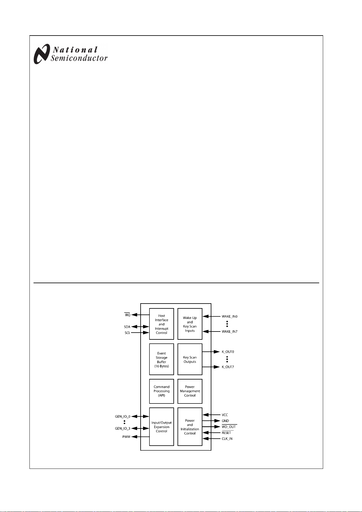
4.0 Block Diagram
20210601
I2C® is a registered trademark of Phillips Corporation.
© 2007 National Semiconductor Corporation 202106 www.national.com
LM8333 Mobile I/O Companion Supporting Key-Scan, I/O Expansion, PWM, and ACCESS.bus
Host Interface
Page 2
5.0 Ordering Information
NSID Spec. No. of Pins Package Type Temperature Package Method
LM8333FLQ8X NOPB 32 LLP −40 to + 85°C 2500 pcs Tape & Reel
LM8333FLQ8Y NOPB 32 LLP −40 to + 85°C 250 pcs Tape & Reel
LM8333GGR8 NOPB 49 Micro-array −40 to + 85°C 1000 pcs Tape & Reel
NOPB = No PB (No Lead)
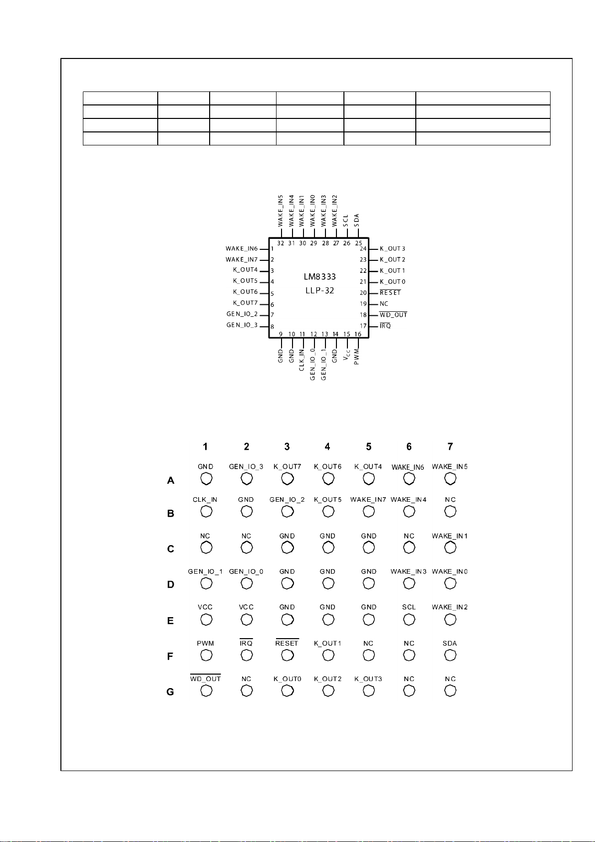
6.0 Pin Assignments
20210649
Top View
Leadless Leadframe Package
See NS Package Number LQA32A
20210602
Top View
MICRO-ARRAY Package
See NS Package Number GRA49A
www.national.com 2
LM8333
Page 3

Table of Contents
1.0 General Description ......................................................................................................................... 1
2.0 Features ........................................................................................................................................ 1
3.0 Applications .................................................................................................................................... 1
4.0 Block Diagram ................................................................................................................................ 1
5.0 Ordering Information ........................................................................................................................ 2
6.0 Pin Assignments ............................................................................................................................. 2
7.0 Signal Descriptions .......................................................................................................................... 4
8.0 Typical Application ........................................................................................................................... 5
8.1 FEATURES .................................................................................................................................. 5
8.2 I/O EXPANSION OPTIONS ............................................................................................................ 5
8.3 WATCHDOG TIMER ..................................................................................................................... 5
8.4 HALT MODE ................................................................................................................................ 5
8.4.1 ACCESS.bus Activity ................................................................................................................ 5
8.5 KEYPAD SCANNING ..................................................................................................................... 6
8.6 COMMUNICATION INTERFACE ..................................................................................................... 6
8.6.1 Interrupts Between the Host and LM8333 ..................................................................................... 6
8.6.2 Interrupt Sources ...................................................................................................................... 6
9.0 Device Operation ............................................................................................................................ 6
9.1 EVENT CODE ASSIGNMENT ......................................................................................................... 6
9.2 I/O EXPANSION ........................................................................................................................... 7
9.2.1 PWM Output with Programmable Duty Cycle ................................................................................ 7
9.2.2 General-Purpose I/O (GPIO) ...................................................................................................... 8
9.2.3 External Interrupts .................................................................................................................... 8
9.3 HOST COMMAND EXECUTION ..................................................................................................... 9
9.3.1 Command Structure .................................................................................................................. 9
9.4 HOST WRITE COMMANDS ......................................................................................................... 10
9.5 HOST READ COMMANDS ........................................................................................................... 10
9.6 WAKE-UP FROM HALT MODE ..................................................................................................... 11
10.0 Interrupts .................................................................................................................................... 11
10.1 INTERRUPT CODE ................................................................................................................... 11
10.2 ERROR CODE .......................................................................................................................... 11
10.3 STATUS CODES ....................................................................................................................... 12
10.4 INTERRUPT PROCESSING ....................................................................................................... 12
10.5 COMMAND EXECUTION SUMMARY .......................................................................................... 13
11.0 Absolute Maximum Ratings ........................................................................................................... 14
12.0 DC Electrical Characteristics ......................................................................................................... 14
13.0 AC Electrical Characteristics ......................................................................................................... 15
14.0 Physical Dimensions .................................................................................................................... 17
3 www.national.com
LM8333
Page 4

7.0 Signal Descriptions
Name 32 Pins 49 Pins I/O Description
WAKE_IN0 29 D7 Input Wake-up input/Keyboard scanning input 0
WAKE_IN1 30 C7 Input Wake-up input/Keyboard scanning input 1
WAKE_IN2 27 E7 Input Wake-up input/Keyboard scanning input 2
WAKE_IN3 28 D6 Input Wake-up input/Keyboard scanning input 3
WAKE_IN4 31 B6 Input Wake-up input/Keyboard scanning input 4
WAKE_IN5 32 A7 Input Wake-up input/Keyboard scanning input 5
WAKE_IN6 1 A6 Input Wake-up input/Keyboard scanning input 6
WAKE_IN7 2 B5 Input Wake-up input/Keyboard scanning input 7
K_OUT0 21 G3 Output Keyboard scanning output 0
K_OUT1 22 F4 Output Keyboard scanning output 1
K_OUT2 23 G4 Output Keyboard scanning output 2
K_OUT3 24 G5 Output Keyboard scanning output 3
K_OUT4 3 A5 Output Keyboard scanning output 4
K_OUT5 4 B4 Output Keyboard scanning output 5
K_OUT6 5 A4 Output Keyboard scanning output 6
K_OUT7 6 A3 Output Keyboard scanning output 7
GEN_IO_0 12 D2 I/O General-purpose I/O 0
GEN_IO_1 13 D1 I/O General-purpose I/O 1
GEN_IO_2 7 B3 I/O General-purpose I/O 2
GEN_IO_3 8 A2 I/O General-purpose I/O 3
SDA 25 F7 I/O ACCESS.bus data signal
SCL 26 E6 Input ACCESS.bus clock signal
IRQ 17 F2 Output Interrupt request output
PWM 16 F1 Output Pulse-width modulated output
WD_OUT 18 G1 Output Watchdog timer output (connect to RESET input)
RESET 20 F3 Input Reset input
CLK_IN 11 B1 Input Clock input (connect to ground through a 68k ohm resistor)
VCC 15 E1, E2 n.a. Vcc
GND 9, 10, 14 A1, B2, C3,
C4, C5, D3,
D4, D5, E3,
E4, E5
n.a. Ground
NC 19 B7, C1, C2,
C6, F5, F6,
G2, G6, G7
n.a. No connect
www.national.com 4
LM8333
Page 5
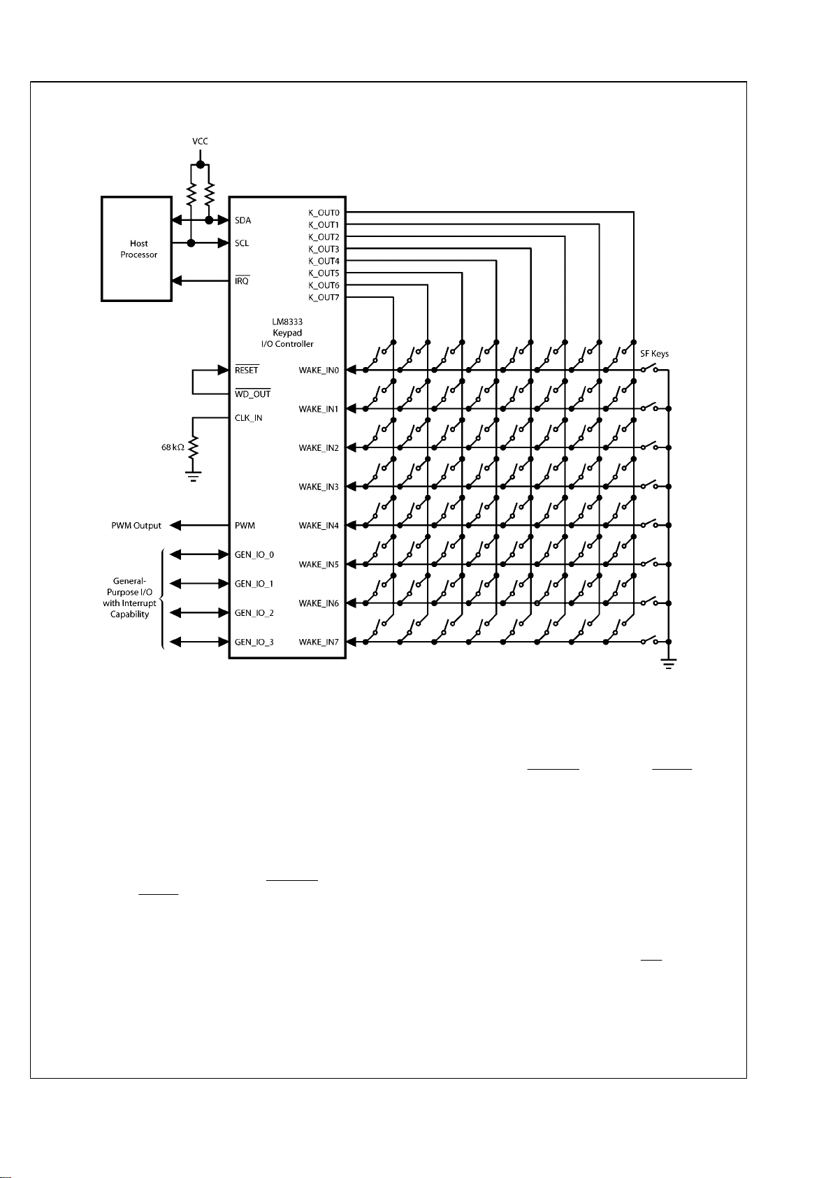
8.0 Typical Application
20210603
FIGURE 1. Typical Keypad Configuration
8.1 FEATURES
The following features are supported:
•
8 x 8 standard keys.
•
8 special function keys (SF keys) with wake-up capability
by forcing a WAKE_INx pin to ground. Pressing a SF key
overrides any other key in the same row.
•
A total of 72 keys can be scanned.
•
ACCESS.bus (I2C-compatible) interface for
communication with the host.
•
The watchdog timer is mandatory, so WD_OUT
must be
connected to RESET.
8.2 I/O EXPANSION OPTIONS
•
One host-programmable PWM output which also may be
used as a general-purpose output.
•
Four host-programmable general-purpose I/O pins,
GEN_IO_0, GEN_IO_1, GEN_IO_2, and GEN_IO_3.
GEN_IO_0 and GEN_IO_1 can also be configured for
“slow” interrupts, in which any transition will trigger a
hardware interrupt event to the host.
8.3 WATCHDOG TIMER
The watchdog timer is always enabled in hardware. To use
the timer, connect the WD_OUT
output to the RESET input.
8.4 HALT MODE
The fully static architecture of the LM8333 allows stopping the
internal RC clock in Halt mode, which reduces power consumption to the minimum level.
Halt mode is entered when no key-press, key-release, or
ACCESS.bus activity is detected for a certain period of time
(by default, 500 milliseconds). The mechanism for entering
Halt mode is always enabled in hardware, but the host can
program the period of inactivity which triggers entry into Halt
mode.
The LM8333 will remain in Active mode as long as a key
event, or any other event, which causes the IRQ output to be
asserted is not resolved.
8.4.1 ACCESS.bus Activity
When the LM8333 is in Halt mode, any activity on the
ACCESS.bus interface will cause the LM8333 to exit from
Halt mode. However, the LM8333 will not be able to acknowl-
5 www.national.com
LM8333
Page 6
edge the first bus cycle immediately following wake-up from
Halt mode. It will respond with a negative acknowledgement,
and the host should then repeat the cycle.
The LM8333 will be prevented from entering Halt mode if it
shares the bus with peripherals that are continuously active.
For lowest power consumption, the LM8333 should only
share the bus with peripherals that require little or no bus activity after system initialization.
8.5 KEYPAD SCANNING
The LM8333 starts new scanning cycles at fixed time intervals
of about 4 ms. If a change in the state of the keypad is detected, the keypad is rescanned after a debounce delay.
When the state change has been reliably captured, it is encoded and written to the FIFO buffer.
If more than two keys are pressed simultaneously, the pattern
of key closures may be ambiguous, so pressing more than
two keys asserts the Error Flag condition and the IRQ output
(if enabled). The host may attempt to interpret the events
stored in the FIFO or discard them.
The SF keys connect the WAKE_INx pins directly to ground.
There can be up to eight SF-keys. If any of these keys are
pressed, other key presses that use the same WAKE_INx pin
will be ignored.
8.6 COMMUNICATION INTERFACE
The two-wire ACCESS.bus interface is used to communicate
with a host. The ACCESS.bus interface is fully compliant with
the I2Cbus standard. The LM8333 operates as a bus slave at
speeds up to 400 kHz.
An ACCESS.bus transfer starts with a byte that includes a 7bit slave device address. The LM8333 responds to a fixed
device address. This address is 0xA2, when aligned to the
MSB (7-bit address mapped to bits 7:1, rather than bits 6:0).
Bit 0 is a direction bit (0 on write, 1 on read).
Because it is a slave, the LM8333 never initiates an
ACCESS.bus cycle, it only responds to bus cycles initiated by
the host. The LM8333 may signal events to the host by asserting the IRQ interrupt request.
8.6.1 Interrupts Between the Host and LM8333
The IRQ output is used to signal unresolved interrupts, errors,
and key-events to the host.
The host can use an available GEN_IO_0 or GEN_IO_1 pin
to interrupt (or wake-up) the LM8333, if it is not being used for
another function. The host can also wake-up the LM8333 by
sending a Start Condition on the ACCESS.bus interface.
Note:
The LM8333 it will not be able to acknowledge the first byte received
from the host after wake-up. In this case, the host will have to resend
the slave address.
8.6.2 Interrupt Sources
The IRQ
output is asserted on these conditions:
•
Any new key-event.
•
Any error condition, which is indicated by the error code.
•
Any enabled interrupt on either of the GEN_IO_0 or
GEN_IO_1 pins that can be configured as external
interrupt inputs. When enabled, any rising or falling edge
triggers an interrupt.
The IRQ output remains asserted until the interrupt code is
read.
9.0 Device Operation
9.1 EVENT CODE ASSIGNMENT
After power-on reset, the LM8333 starts scanning the keypad.
It stays active for a default time of about 500 ms after the last
key is released, after which it enters a standby mode to minimize power consumption (<2 µA standby current).
Table 1 lists the codes assigned to the matrix positions encoded by the hardware. Key-press events are assigned the
codes listed in Table 1, but with the MSB set. When a key is
released, the MSB of the code is clear.
TABLE 1. Keypad Matrix Code Assignments
K_OUT0 K_OUT1 K_OUT2 K_OUT3 K_OUT4 K_OUT5 K_OUT6 K_OUT7 SF Keys
WAKE_IN0 0x01 0x02 0x03 0x04 0x05 0x06 0x07 0x08 0x09
WAKE_IN1 0x11 0x12 0x13 0x14 0x15 0x16 0x17 0x18 0x19
WAKE_IN2 0x21 0x22 0x23 0x24 0x25 0x26 0x27 0x28 0x29
WAKE_IN3 0x31 0x32 0x33 0x34 0x35 0x36 0x37 0x38 0x39
WAKE_IN4 0x41 0x42 0x43 0x44 0x45 0x46 0x47 0x48 0x49
WAKE_IN5 0x51 0x52 0x53 0x54 0x55 0x56 0x57 0x58 0x59
WAKE_IN6 0x61 0x62 0x63 0x64 0x65 0x66 0x67 0x68 0x69
WAKE_IN7 0x71 0x72 0x73 0x74 0x75 0x76 0x77 0x78 0x79
The codes are loaded into the FIFO buffer in the order in
which they occurred. Table 2 shows an example sequence of
events, and Figure 2 shows the resulting sequence of event
codes loaded into the FIFO buffer.
www.national.com 6
LM8333
Page 7

TABLE 2. Example Sequence of Events
Event Number Event Code Event on Input Matrix Node Description
1 0xF1 Wake_INP7 K_OUT0 Key is pressed
2 0xB6 Wake_INP3 K_OUT5 Key is pressed
3 0x71 Wake_INP7 K_OUT0 Key is released
4 0x36 Wake_INP3 K_OUT5 Key is released
5 0xB4 Wake_INP3 K_OUT3 Key is pressed
6 0x34 Wake_INP3 K_OUT3 Key is released33
7 0x91 Wake_INP1 K_OUT0 Key is pressed
8 0x00 NA NA Indicates end of stored events
20210604
FIGURE 2. Example Event Codes Loaded in FIFO Buffer
9.2 I/O EXPANSION
In addition to keypad scanning, the LM8333 supports various
I/O expansion options.
9.2.1 PWM Output with Programmable Duty Cycle
The PWM pin may be used either as a pulse-width modulated
output driven by a 16-bit timer or as a general-purpose output
pin. In the PWM mode, the low time (TLO) and high time
(THI) are programmable between 1 × tC and 65K × tC cycles
in which tC is the cycle time (nominally 1 microsecond), as
shown in Figure 3. The period TPD is the sum of THI and TLO.
The PWM_LO command writes TLO, and the PWM_HI command writes THI. Operational modes of the PWM pin are
controlled by the PWM_CTL command. Before activating the
PWM output, the TLO and THI times must be initialized. Figure
4 shows the command formats.
20210605
FIGURE 3. Programmable PWM
20210606
FIGURE 4. PWM Control Commands for Arbitrary Duty Cycle
7 www.national.com
LM8333
Page 8

TABLE 3. Summary of PWM Control Bits
OUT_DIR Bit PWM_DIR Bit MOD BIT Description
0 1 0 Drive output low
1 1 0 Drive output high
0 0 0 TRI-STATE® mode
X X 1 PWM timer output
9.2.2 General-Purpose I/O (GPIO)
Figure 5 shows the commands to write, read and control the
general-purpose I/O port pins, GEN_IO_0, GEN_IO_1,
GEN_IO_2, and GEN_IO_3.
All general-purpose I/O pins can be programmed as inputs or
outputs as shown in Table 4. The GEN_IO_0 and GEN_IO_1
pins provide an additional capability for programmable wakeup.
20210607
FIGURE 5. General-Purpose I/O Control Commands
Table 4 shows the pin configuration for all four combinations
of control bit settings (data output and direction) for the general-purpose I/O pins. GEN_IO_3 cannot be put into the high
impedance (Hi-Z) input mode. When programmed as an input, it can only be configured as an input with a weak pullup.
TABLE 4. General Purpose I/O Pin Configuration
GEN_IO_DIR Bit GEN_IO_OUT Bit Direction State
0 0 Input Hi-Z
0 1 Input Weak Pullup
1 0 Output Drive Low
1 1 Output Drive High
9.2.3 External Interrupts
When the GEN_IO_0 or GEN_IO_1 pins are configured as
inputs, a SET_EXT_INT command (0xD1) can be used to
enable receiving external interrupts on either or both of these
pins. Setting the EX_0 or EX_1 bits in the data byte of the
SET_EXT_INT command (as shown in Figure 6) enables the
corresponding pin as an external interrupt input. When enabled as an interrupt input, any rising or falling edge causes
the IRQ
output to be asserted. If the LM8333 was in Halt
mode, it also wakes up into Active mode.
20210608
FIGURE 6. SET_EXT_INT Command Data Byte
When both GEN_IO_0 and GEN_IO_1 are configured as interrupt inputs, bits 1 and 2 of the interrupt code indicate which
input asserted the interrupt. However, if only one of
GEN_IO_0 or GEN_IO_1 is configured as an interrupt input,
both bits 1 and 2 of the interrupt code will be set when an
interrupt occurs.
www.national.com 8
LM8333
Page 9

TABLE 5. Interface Commands for Controlling the LM8333
Function Cmd Dir Data Bits Data Description
FIFO_READ 0x20 R 128
Event Codes from
FIFO
Read an event from the FIFO.
Maximum 14 event codes stored in the FIFO.
MSB = 1: key pressed.
MSB = 0: key released.
RPT_FIFO_READ 0x21 R 128
Event Codes from
FIFO
Repeats a FIFO read without advancing the FIFO pointer,
for example to retry a read after an error.
Maximum 14 event codes stored in the FIFO.
MSB = 1: key pressed.
MSB = 0: key released.
DEBOUNCE 0x22 W 8 nnnn nnnn
Default is 10 ms. Valid range 1–255.
Time ~ n × 3 ms
GEN_IO_IN 0x30 R 8 0000 nnnn Read port data.
GEN_IO_OUT 0x31 W 8 0000 nnnn
Specify port mode. (Drive 0 or 1 when the port is configured
as an output; select Hi-Z or pullup when the port is
configured as an input.)
GEN_IO_DIR 0x32 W 8 0000 nnnn Select port direction (input or output).
PWM_HI 0x40 W 16
(n+1) × t
C
Sets the low pulse time of the PWM signal.
PWM_LO 0x41 W 16
(n+1) × t
C
Sets the high pulse time of the PWM signal.
PWM_CTL 0x42 W 8 0000 0nnn Activate, reactivate, or stop PWM.
READ_INT 0xD0 R 8 0000 nnnn
Reads the interrupt code, acknowledges the interrupt,
deasserts the IRQ output, and clears the code.
SET_EXT_INT 0xD1 W 8 0000 00nn
Enables/disables external interrupts on GEN_IO_0 and
GEN_IO_1.
READ_STAT 0xE0 R 8 000n nnnn Status Information.
SCAN_REQ 0xE3 W 8
Requests rescanning the keypad (for example, after an
error was reported).
ACTIVE 0xE4 W 8 nnnn nnnn
Specifies the time after the last event during which the
LM8333 stays active before entering Halt mode. The active
time must be greater than the debounce time.
Default is 500 msec
Valid range for n is 1–255
Time ~ n × 3 msec.
READ_ERROR 0xF0 R 8 0nnn nnnn Reads and clears the error code.
9.3 HOST COMMAND EXECUTION
9.3.1 Command Structure
All communication with the LM8333 over the ACCESS.bus
interface is initiated by the host, usually in response to an in-
terrupt request (IRQ low) asserted by the LM8333. Figure 7
shows a sequence of Start conditions, slave addresses,
READ_INT command (0xD0), acknowledge cycles, data
bytes, and Stop condition for reading the interrupt code.
20210609
FIGURE 7. Typical Command Sequence from Host
9 www.national.com
LM8333
Page 10

Every transfer is preceded by a Start condition (S) or a Repeated Start condition (RS). The latter occurs when a command follows immediately upon another command without an
intervening Stop condition (P). A Stop condition indicates the
end of transmission. Every byte is acknowledged (A) by the
receiver.
The first byte in a write from the host to the LM8333 is 0xA2,
and the first byte in a read is 0xA3. This byte is composed of
a 7-bit slave address in bits 7:1 and a direction bit in bit 0. The
direction bit is 0 on writes from the host to the slave and 1 on
reads from the slave to the host.
The second byte sends the command. The commands are
listed in Table 5. In the example, the READ_INT command
(0xD0) reads the interrupt code.
The slave address is repeated in the third byte, with the direction bit set to 1. The Start (or Repeated Start) condition
must be repeated whenever the slave address or the direction
bit is changed. In this case, the direction bit is changed.
The data is sent from the slave to the host in the fourth byte.
When the master is the receiver, it sends a negative acknowledgement (NA) to indicate the end of the data.
9.4 HOST WRITE COMMANDS
Some host commands include one or more data bytes written
to the LM8333. Figure 8 shows a SET_EXT_INT command,
which consists of an address byte, a command byte, and one
data byte.
The first byte is composed of a 7-bit slave address in bits 7:1
and a direction bit in bit 0. The state of the direction bit is 0 on
writes from the host to the slave and 1 on reads from the slave
to the host.
The second byte sends the command. The commands are
listed in Figure 9. The SET_EXT_INT command is 0xD1.
The third byte send the data, in this case configuring
GEN_IO_0 as an external interrupt input.
20210610
FIGURE 8. Host Write Command
9.5 HOST READ COMMANDS
Some host commands include one or more data bytes read
from the LM8333. Figure 9 shows a READ_INT command
which consists of an address byte, a command byte, a second
address byte, and a data byte.
The first address byte is sent with the direction bit driven low
to indicate a write transaction of the command to the LM8333.
The second address byte is sent with the direction bit undriven
(pulled high) to indicate a read transaction of the data from
the LM8333.
The Start (or Repeated Start) condition must be repeated
whenever the slave address or the direction bit is changed. In
this case, the direction bit is changed.
The data is sent from the slave to the host in the fourth byte.
This byte ends with a negative acknowledgement (NACK) to
indicate the end of the data.
20210611
FIGURE 9. Host Read Command
www.national.com 10
LM8333
Page 11

9.6 WAKE-UP FROM HALT MODE
Any bus transaction initiated by the host may encounter the
LM8333 device in Halt mode or busy with processing data,
such as controlling the FIFO buffer or executing interrupt service routines.
Figure 10 shows the case in which the host sends a command
while the LM8333 is in Halt mode (CPU clock is stopped). Any
activity on the ACCESS.bus wakes up the LM8333, but it
cannot acknowledge the first bus cycle immediately after
wake-up.
The host drives a Start condition followed by seven address
bits and a R/W bit. The host then releases SDA for one clock
period, so that it can be driven by the LM8333.
If the LM8333 does not drive SDA low during the high phase
of the clock period immediately after the R/W bit, the bus cycle
terminates without being acknowledged (shown as NACK in
Figure 10). The host then aborts the transaction by sending
a Stop condition. After aborting the bus cycle, the host may
then retry the bus cycle. On the second attempt, the LM8333
will be able to acknowledge the slave address, because it will
be in Active mode.
Alternatively, the I2C specification allows sending a START
byte (00000001), which will not be acknowledged by any device. This byte can be used to wake up the LM8333 from Halt
mode.
The LM8333 may also stall the bus transaction by pulling the
SCL low, which is a valid behavior defined by the I2C specification.
20210612
FIGURE 10. LM8333 Responds with NACK, Host Retries Command
10.0 Interrupts
10.1 INTERRUPT CODE
The interrupt code is read and acknowledged with the
READ_INT command (0xD0). This command clears the code
and deasserts the IRQ
output. Table 6 shows the format of
the interrupt code.
Note that when only one of the interrupt-capable pins
GEN_IO_0 or GEN_IO_1 is configured as an interrupt input,
bits 1 and 2 are both set when an interrupt occurs. When both
GEN_IO_0 and GEN_IO_1 pins are configured as interrupt
inputs, only one bit corresponding to the interrupt source is
set when an interrupt occurs.
TABLE 6. Interrupt Code
7 6 5 4 3 2 1 0
0 0 0 0 ERROR EX_1 EX_0 KEYPAD
Bit Description
ERROR An error condition occurred.
EX_1 A rising or falling edge was detected on GEN_IO_1.
EX_0 A rising or falling edge was detected on GEN_IO_0.
KEYPAD A key-press or key-release event occurred.
10.2 ERROR CODE
If the LM8333 reports an error, the READ_ERROR command
(0xF0) is used to read and clear the error code. Table 7 shows
the format of the error code.
TABLE 7. Error Code
7 6 5 4 3 2 1 0
0 FIFOOVR 0 NOINT 0 KEYOVR CMDUNK CMDOVR
11 www.national.com
LM8333
Page 12

Bit Description
FIFOOVR Key event occurred while the FIFO was full.
NOINT Interrupt deasserted before it could be serviced.
KEYOVR More than two keys were pressed simultaneously.
CMDUNK Not a valid command.
CMDOVR Command received before it could be accepted, e.g. after wake-up.
10.3 STATUS CODES
The host can use the READ_STAT command (0xE0) to read
the status code, for example to synchronize after an error.
TABLE 8. Status Codes
Status Code Description
Reset 0000 0000 Default after reset.
Wake Up Interrupt 0000 0010 Wake-up caused by external interrupt.
Ack 0000 0110 Last host command was successful.
NoAck 0001 0101 Last host command was not successful.
10.4 INTERRUPT PROCESSING
Unexpected states encountered during run-time, for example
overrun of the FIFO buffer, are reported as errors. When the
host receives an interrupt from the LM8333, it uses a
READ_INT command to read the interrupt code. If the code
has a set ERROR bit, the host then uses a READ_ERROR
command to read the error code, as shown in Figure 11.
20210613
FIGURE 11. Interrupt Processing
www.national.com 12
LM8333
Page 13

10.5 COMMAND EXECUTION SUMMARY
•
With the interrupt, status, and error codes, the LM8333
provides the features needed to support a reliable keyscan functionality.
•
Up to 14 key-scan events can be stored in an internal FIFO
buffer. The end of buffer is indicated with the 00 (empty
character) code.
•
The host can repeatedly read the FIFO without modifying
the FIFO pointer using the RPT_FIFO_READ command
(0x21), for example if an error is encountered during a
read.
•
The LM8333 asserts the IRQ
output low when a new
character is pressed after the last interrupt acknowledge
from the host. The IRQ output will be deasserted after the
host has acknowledged the interrupt by reading the
interrupt code using the READ_INT command (0xD0).
•
The host can synchronize with the LM8333 by reading the
status code with the READ_STAT command (0xE0). The
status code verifies whether the last command was
successfully completed.
•
Two GPIO pins on the LM8333 may be configured as
external interrupt inputs. A rising or falling edge on an
enabled interrupt input triggers wake-up from Halt mode
and asserts an interrupt to the host by pulling the IRQ
output low.
•
The host can change the debounce time from the default
time of 10 ms. This can be used for reliable scanning of
keyboards with noisy contacts. The debounce time can be
set to about 1 second in steps of 4 milliseconds. The
debounce time is set with the DEBOUNCE command
(0x22).
•
The host can change the active time permitted before
entering Halt mode from the default period of 500 ms. The
active time is the time during which the keypad is scanned
after the last key is released, before entering Halt mode.
The active time must be longer than the debounce time.
•
The host can program the direction and output state of four
general-purpose I/O pins. The host can also read the
states on these pins.
•
The host can program a 16-bit timer for generating a PWM
output. If the PWM function is not used, the PWM pin can
be used as a general-purpose output.
13 www.national.com
LM8333
Page 14

11.0 Absolute Maximum Ratings (Note
1)
If Military/Aerospace specified devices are required,
please contact the National Semiconductor Sales Office/
Distributors for availability and specifications.
Supply Voltage (VCC)
3.5V
Voltage at Any Pin -0.3V to VCC +0.3V
Maximum Input Current Without
Latchup ±100 mA
ESD Protection Level
Human Body Model 2 kV
Machine Model 200V
Total Current into VCC Pin
(Source) 80 mA
Total Current out of GND Pin (Sink) 60 mA
Storage Temperature Range −65°C to +140°C
12.0 DC Electrical Characteristics
(Temperature: -40°C ≤ TA ≤ +85°C)
Data sheet specification limits are guaranteed by design, test, or statistical analysis.
Symbol Parameter Conditions
Min
(Note 2)
Typ
Max
(Note 2)
Units
V
CC
Operating Voltage 2.25 2.9 V
Power Supply Rise Time from 0.0V 20 µs 10 ms
(On Chip Power-On Reset Selected)
I
DD
Supply Current (Note 3) RC Clock = 10 MHz, 6 mA
VCC = 2.75V, TC = 1 µs (Note
4)
I
HALT
Standby Mode Current (Note 5) VCC = 2.75V, TC = 0 µs, (Note
4), TA = 25°C
<2 15 µA
V
IL
Logical 0 Input Voltage 0.25 V
CC
V
V
IH
Logical 1 Input Voltage 0.8 V
CC
V
Hi-Z Input Leakage (TRI-STATE Output) VCC = 2.75V -0.1 0.1 µA
Input PullupCurrent VCC = 2.75V, VIN = 0V -15 -120 µA
Port Input Hysteresis (Note 6) 0.1 V
Output Current Source (Weak Pull-Up) VCC = 2.25V, VOH = 1.7V -10 -80 µA
Output Current Source (Push-Pull Mode) VCC = 2.25V, VOH = 1.7V -10 mA
Output CurrentSink (Push-Pull Mode) VCC = 2.25V, VOL = 0.4V 10 mA
Allowable Sink and Source Current per Pin 16 mA
C
PAD
Input Capacitance 8.5 pF
Note 1: Absolute Maximum Ratings indicate limits beyond which damage to the device may occur. Operating Ratings indicate conditions for which the device is
intended to be functional, but specific performance is not guaranteed. For guaranteed specifications and test conditions, see the Electrical Characteristics tables.
Note 2: Data sheet minimum and maximum limits are guaranteed by design, test, or statistical analysis.
Note 3: Supply current is measured with inputs connected to VCC and outputs driven low but not connected to a load.
Note 4: TC = instruction cycle time (min. 0.7 µs).
Note 5: In Halt mode, the internal clock is switched off. Supply current in Halt mode is measured with inputs connected to VCC and outputs driven low but not
connected to a load.
Note 6: Guaranteed by design, not tested.
www.national.com 14
LM8333
Page 15

13.0 AC Electrical Characteristics
(Temperature: -40°C ≤ TA ≤ +85°C)
Data sheet specification limits are guaranteed by design, test, or statistical analysis.
Symbol Parameter Conditions
Min
(Note 7)
Typ
Max
(Note 7)
Units
Internal Oscillator
External R from CLK_IN to Gnd (R
= 68 kohm)
0.75 µs
2.25V ≤ VCC ≤ 2.75V
System Oscillator (mclk)
External R from CLK_IN to Gnd (R
= 68 kohm)
2.25V ≤ VCC ≤ 2.75V
75 ns
System Oscillator and Internal
Frequency Variation
2.25V ≤ VCC ≤ 2.75V
±30 %
Input Pulse Width Low 0.7 µs
Input Pulse Width High 0.7 µs
ACCESS.bus Input Timing (Note 8)
t
BUFi
Bus free time between Stop and
Start Condition
t
SCLhigho
t
CSTOHsi
SCL setup time Before Stop Condition 8 mclk
t
CSTRHhi
SCL hold time After Start Condition 8 mclk
t
DHCsi
Data High setup time Before SCL Rising Edge (RE) 2 mclk
t
DLCsi
Data Low setup time Before SCL RE 2 mclk
t
SCLlowi
SCL low time After SCL Falling Edge (FE) 12 mclk
t
SCLhighi
SCL high time After SCL RE 12 mclk
t
SDAhi
SDA hold time After SCL FE 0 ns
t
SDAsi
SDA setup time Before SCL RE 2 mclk
ACCESS.bus Output Timing (Note 8)
t
BUFo
Bus free time between Stop and
Start Condition
t
SCLhigho
t
CSTOso
SCL setup time Before Stop Condition t
SCLhigho
t
CSTRho
SCL hold time After Start Condition t
SCLhigho
t
CSTRso
SCL setup time Before Start Condition t
SCLhigho
t
DHCso
Data High setup time Before SCL RE t
SCLhigho
t
DLCso
Data Low setup time Before SCL RE t
SCLhigho
t
SCLlowo
SCL low time After SCL FE 16 mclk
t
SCLhigho
SCL high time After SCL RE 16 mclk
t
SDAho
SDA hold time After SCL FE 7 mclk
t
SDAvo
SDA valid time Before SCL FE 7 mclk
Note 7: Data sheet minimum and maximum limits are guaranteed by design, test, or statistical analysis.
Note 8: The ACCESS.bus interface of the LM8333 device implements and meets the timing necessary for interface to the I2C bus and SMBus protocol at logic
levels. The bus drivers are designed with open-drain output as required for bidirectional operation. The LM8333 device will not meet the AC timing and current/
voltage requirements of the full bus specification.
15 www.national.com
LM8333
Page 16

20210614
FIGURE 12. ACCESS.bus Start and Stop Condition Timing
www.national.com 16
LM8333
Page 17

14.0 Physical Dimensions inches (millimeters) unless otherwise noted
Leadless Leadframe Package
Order Number LM8333FLQ8X or LM8333FLQ8Y
NS Package Number LQA32A
Micro Array Package
Order Number LM8333GGR8
NS Package Number GRA49A
17 www.national.com
LM8333
Page 18

Notes
LM8333 Mobile I/O Companion Supporting Key-Scan, I/O Expansion, PWM, and ACCESS.bus
Host Interface
THE CONTENTS OF THIS DOCUMENT ARE PROVIDED IN CONNECTION WITH NATIONAL SEMICONDUCTOR CORPORATION
(“NATIONAL”) PRODUCTS. NATIONAL MAKES NO REPRESENTATIONS OR WARRANTIES WITH RESPECT TO THE ACCURACY
OR COMPLETENESS OF THE CONTENTS OF THIS PUBLICATION AND RESERVES THE RIGHT TO MAKE CHANGES TO
SPECIFICATIONS AND PRODUCT DESCRIPTIONS AT ANY TIME WITHOUT NOTICE. NO LICENSE, WHETHER EXPRESS,
IMPLIED, ARISING BY ESTOPPEL OR OTHERWISE, TO ANY INTELLECTUAL PROPERTY RIGHTS IS GRANTED BY THIS
DOCUMENT.
TESTING AND OTHER QUALITY CONTROLS ARE USED TO THE EXTENT NATIONAL DEEMS NECESSARY TO SUPPORT
NATIONAL’S PRODUCT WARRANTY. EXCEPT WHERE MANDATED BY GOVERNMENT REQUIREMENTS, TESTING OF ALL
PARAMETERS OF EACH PRODUCT IS NOT NECESSARILY PERFORMED. NATIONAL ASSUMES NO LIABILITY FOR
APPLICATIONS ASSISTANCE OR BUYER PRODUCT DESIGN. BUYERS ARE RESPONSIBLE FOR THEIR PRODUCTS AND
APPLICATIONS USING NATIONAL COMPONENTS. PRIOR TO USING OR DISTRIBUTING ANY PRODUCTS THAT INCLUDE
NATIONAL COMPONENTS, BUYERS SHOULD PROVIDE ADEQUATE DESIGN, TESTING AND OPERATING SAFEGUARDS.
EXCEPT AS PROVIDED IN NATIONAL’S TERMS AND CONDITIONS OF SALE FOR SUCH PRODUCTS, NATIONAL ASSUMES NO
LIABILITY WHATSOEVER, AND NATIONAL DISCLAIMS ANY EXPRESS OR IMPLIED WARRANTY RELATING TO THE SALE
AND/OR USE OF NATIONAL PRODUCTS INCLUDING LIABILITY OR WARRANTIES RELATING TO FITNESS FOR A PARTICULAR
PURPOSE, MERCHANTABILITY, OR INFRINGEMENT OF ANY PATENT, COPYRIGHT OR OTHER INTELLECTUAL PROPERTY
RIGHT.
LIFE SUPPORT POLICY
NATIONAL’S PRODUCTS ARE NOT AUTHORIZED FOR USE AS CRITICAL COMPONENTS IN LIFE SUPPORT DEVICES OR
SYSTEMS WITHOUT THE EXPRESS PRIOR WRITTEN APPROVAL OF THE CHIEF EXECUTIVE OFFICER AND GENERAL
COUNSEL OF NATIONAL SEMICONDUCTOR CORPORATION. As used herein:
Life support devices or systems are devices which (a) are intended for surgical implant into the body, or (b) support or sustain life and
whose failure to perform when properly used in accordance with instructions for use provided in the labeling can be reasonably expected
to result in a significant injury to the user. A critical component is any component in a life support device or system whose failure to perform
can be reasonably expected to cause the failure of the life support device or system or to affect its safety or effectiveness.
National Semiconductor and the National Semiconductor logo are registered trademarks of National Semiconductor Corporation. All other
brand or product names may be trademarks or registered trademarks of their respective holders.
Copyright© 2007 National Semiconductor Corporation
For the most current product information visit us at www.national.com
National Semiconductor
Americas Customer
Support Center
Email:
new.feedback@nsc.com
Tel: 1-800-272-9959
National Semiconductor Europe
Customer Support Center
Fax: +49 (0) 180-530-85-86
Email: europe.support@nsc.com
Deutsch Tel: +49 (0) 69 9508 6208
English Tel: +49 (0) 870 24 0 2171
Français Tel: +33 (0) 1 41 91 8790
National Semiconductor Asia
Pacific Customer Support Center
Email: ap.support@nsc.com
National Semiconductor Japan
Customer Support Center
Fax: 81-3-5639-7507
Email: jpn.feedback@nsc.com
Tel: 81-3-5639-7560
www.national.com
 Loading...