

Page 1
LM831 Low Voltage Audio Power Amplifier
LM831 Low Voltage Audio Power Amplifier
December 1994
General Description
The LM831 is a dual audio power amplifier optimized for
very low voltage operation. The LM831 has two independent amplifiers, giving stereo or higher power bridge (BTL)
operation from two- or three-cell power supplies.
The LM831 uses a patented compensation technique to reduce high-frequency radiation for optimum performance in
AM radio applications. This compensation also results in
lower distortion and less wide-band noise.
The input is direct-coupled to the LM831, eliminating the
usual coupling capacitor. Voltage gain is adjustable with a
single resistor.
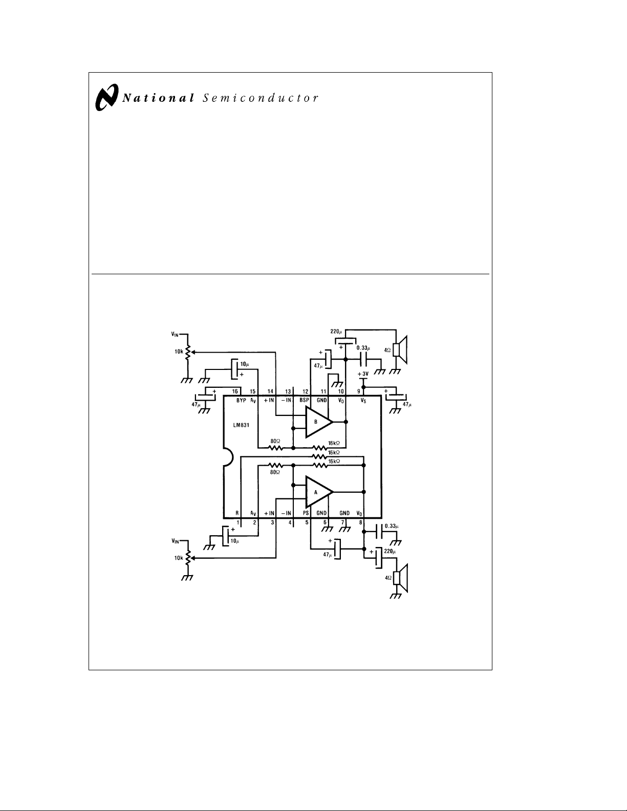
Typical Application
Dual Amplifier with Minimum Parts
Features
Y
Low voltage operation, 1.8V to 6.0V
Y
High power, 440 mW, 8X, BTL, 3V
Y
Low AM radiation
Y
Low noise
Y
Low THD
Applications
Y
Portable tape recorders
Y
Portable radios
Y
Headphone stereo
Y
Portable speakers
TL/H/6754– 1
e
A
46 dB,BWe250 Hz to 35 kHz
V
e
P
220 mW/Ch,R
OUT
C
1995 National Semiconductor Corporation RRD-B30M115/Printed in U. S. A.
TL/H/6754
e
4X
L
Page 2
Absolute Maximum Ratings
If Military/Aerospace specified devices are required,
please contact the National Semiconductor Sales
Office/Distributors for availability and specifications.
Supply Voltage, V
Input Voltage, V
Power Dissipation (Note 1), P
S
IN
D
Operating Temperature (Note 1), T
1.3W (M Package)
1.4W (N Package)
b
opr
40§Ctoa85§C
7.5V
g
0.4V
b
Storage Temperature, T
Junction Temperature, T
Lead Temp. (Soldering, 10 sec.), T
stg
j
Thermal Resistance
i
(DIP) 27§C/W
JC
i
(DIP) 75§C/W
JA
i
(SO Package) 20§C/W
JC
i
(SO Package) 95§C/W
JA
65§Ctoa150§C
L
a
a
150§C
260§C
Electrical Characteristics
Unless otherwise specified, T
e
25§C, V
A
Symbol Parameter Conditions Typ Tested Limit Unit (Limit)
V
S
I
Q
V
OS
R
IN
A
V
Operating Voltage 3 1.8 V(Min)
Supply Current V
Output DC Offset V
Input Resistance 25 15 k (Min)
Voltage Gain V
PSRR Supply Rejection V
P
OD
P
ODL
P
OB
P
OBL
Power Out V
Power Out Low, V
S
Power Out V
Power Out Low, V
S
Sep Channel Separation Referenced to V
I
B
E
n0
Input Bias Current 1 2 mA (Max)
Output Noise Wide Band (250E35 kHz) 250 500 mV (Max)
THD Distortion V
Note 1: For operation in ambient temperatures above 25§C, the device must be derated based on a 150§C maximum junction temperature and a thermal resistance
C/W junction to ambient for the M package or 90§C/W junction to ambient for the N package.
of 98
§
e
3V, fe1 kHz, test circuit is dual or BTL amplifier with minimum parts.
S
3 6 V(Max)
e
0, Dual Mode 5 10 mA (Max)
IN
e
0, BTL Mode 6 15 mA (Max)
V
IN
e
0, BTL Mode 10 50 mV (Max)
IN
35 k (Max)
e
2.25 mV
IN
Dual Mode 48 dB (Max)
e3Va
S
e
3V, R
S
10% THD, Dual Mode
e
V
1.8V, R
S
10% THD, Dual Mode
e
3V, R
S
10% THD, BTL Mode
e
V
1.8V, R
S
10% THD, BTL Mode
e
3V, P
S
e
f
1 kHz, Dual
,fe1 kHz, 46 44 dB (Min)
rms
4X,
e
4X,
8X,
e
8X,
e
O
50 mW,
@
fe1 kHz 46 30 dB (Min)
rms
220 150 mW (Min)
45 10 mW (Min)
440 300 mW (Min)
90 20 mW (Min)
200 mV
rms
52 40 dB (Min)
0.25 1 % (Max)
200 mV
e
L
L
e
L
L
e
O
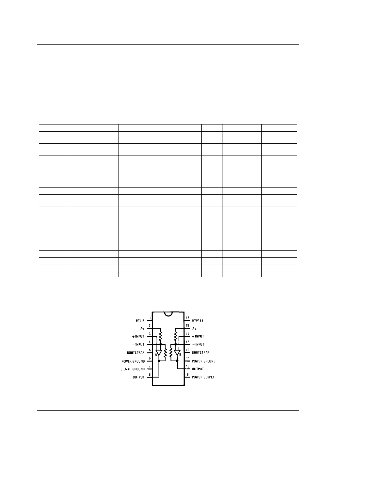
Connection Diagram
Dual-In-Line Package
TL/H/6754– 2
Top View
Order Number LM831M or N
See NS Package Number M16B or N16E
2
Page 3
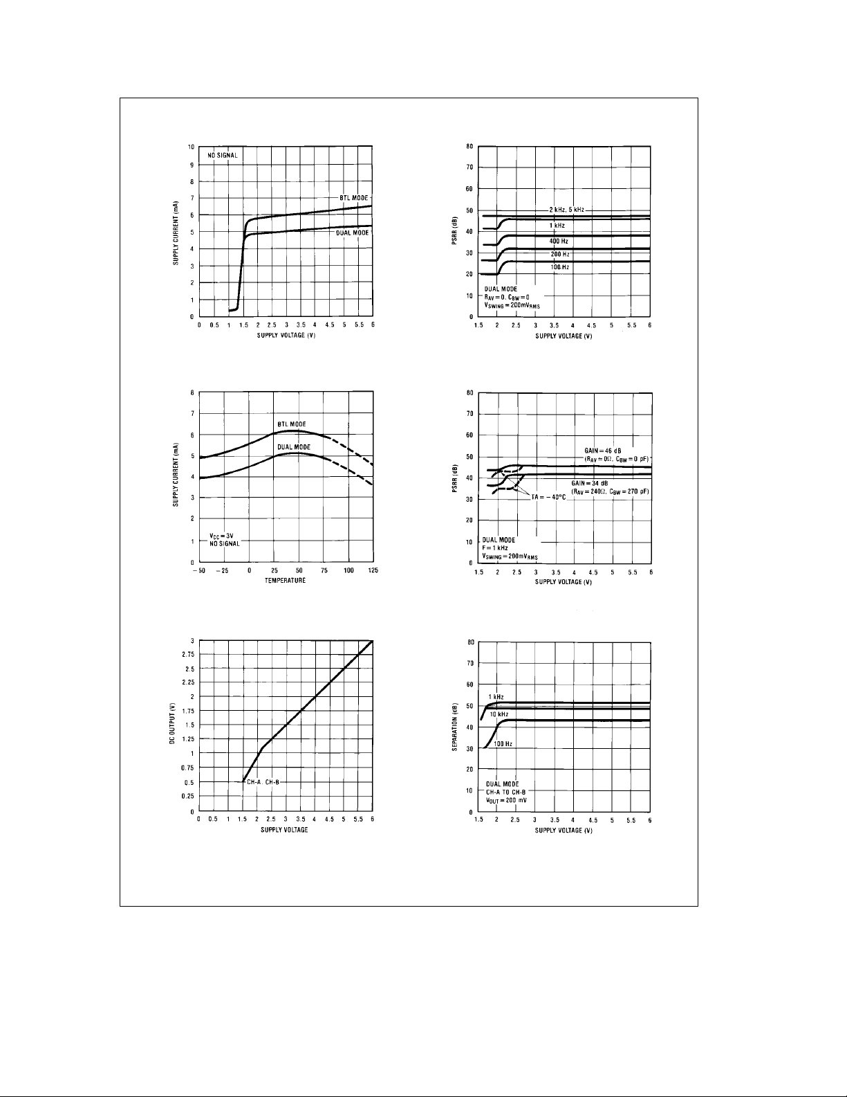
Typical Performance Characteristics
Supply Current vs Supply Voltage PSRR vs Supply Voltage
Supply Current vs Temperature PSRR vs Supply Voltage
DC Output vs Supply Voltage Separation vs Supply Voltage
3
TL/H/6754– 4
Page 4
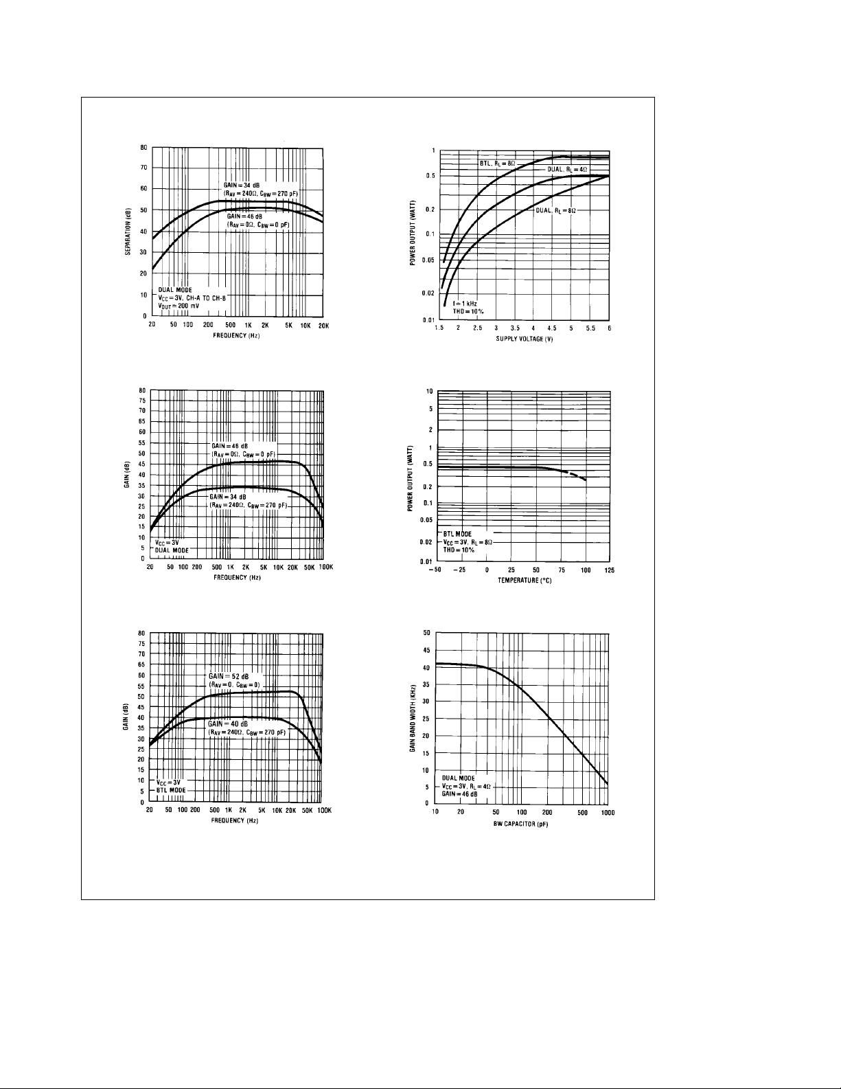
Typical Performance Characteristics (Continued)
Separation vs Frequency Power Output vs Supply Voltage
Gain vs Frequency Power Output vs Temperature
Gain vs Frequency Bandwidth vs BW Capacitance
4
TL/H/6754– 5
Page 5
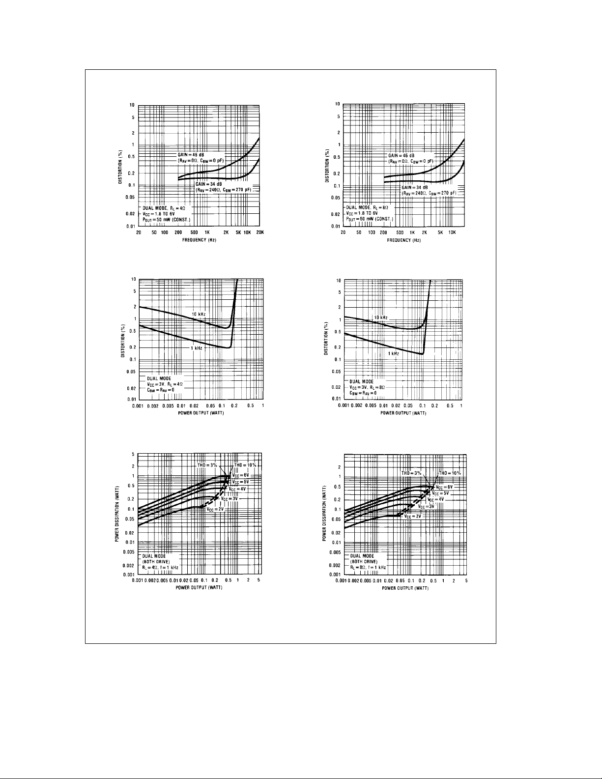
Typical Performance Characteristics (Continued)
e
Dual Mode, R
Distortion vs Power Output (Note 2) Distortion vs Power Output (Note 2)
4X Distortion vs Frequency Dual Mode, R
L
e
8X Distortion vs Frequency
L
Power Dissipation vs Power Output Power Dissipation vs Power Output
5
TL/H/6754– 6
Page 6

Typical Performance Characteristics (Continued)
e
BTL Mode, R
Distortion vs Power Output (Note 2) Supply Current vs Power Output
8X Distortion vs Frequency Device Dissipation vs Ambient Temperature
L
Power Dissipation vs Power Output
Note 2: 1 kHz curve is measured with 400 Hz– 30 kHz Filter.
TL/H/6754– 7
6
Page 7

Typical Applications
BTL Amplifier with Minimum Parts
e
A
52 dB, BWe250 Hz to 25 kHz
V
e
P
440 mW, R
OUT
e
8X
L
BTL Amplifier for Hi-Fi Quality
e
A
40 dB, BWe20 Hz to 20 kHz
V
e
P
440 mW, R
OUT
(Dynamic Range Over 80 dB)
e
8X
L
TL/H/6754– 8
TL/H/6754– 9
7
Page 8

Typical Applications (Continued)
Dual Amplifier for Hi-Fi Quality
e
A
34 dB, BWe50 Hz to 20 kHz
V
e
P
220 mW/Ch, R
OUT
(Dynamic Range Over 80 dB)
e
4X
L
Low-Cost Power Amplifier (No Bootstrap)
e
P
150 mW/Ch, BWe300 Hz to 35 kHz
OUT
*For 3-cell applications, the 120k resistor should be changed to 20K.
BTL Mode is also possible
TL/H/6754– 10
TL/H/6754– 11
8
Page 9

LM831 Circuit Description Refer to the external component diagram and equivalent schematic.
The power supply is applied to Pin 9 and is filtered by resistor R
and capacitor CBYon Pin 16. This filtered voltage at
1
Pin 16 is used to bias all of the LM831 circuits except the
power output stage. Resistor R
that sets the output DC voltage for optimum output power
generates a biasing current
0
for any given supply voltage.
Feedback is provided to the input transistor Q
R
and R7.
6
emitter by
1
External Component Diagram
The capacitor C
mum DC accuracy.
Q
provides voltage gain and the rest of the devices buffer
2
the output load from Q
on Pin 2 provides unity DC gain for maxi-
NF
’s collector.
2
Bootstrapping of Pin 5 by CBSallows maximum output
swing and improved supply rejection.
R
is provided for bridge (BTL) operation.
5
TL/H/6754– 12
9
Page 10

LM831 Circuit Description (Continued)
TL/H/6754– 13
LM831 Equivalent Schematic
10
Page 11

External Components (Refer to External Component Diagram)
Component Comments Min Max
C
O
C
c
C
BS
C
S
C
BY
C
NF
C
BTL
C
BW
R
AV
Required to stabilize output stage. 0.33 mF1mF
Output coupling capacitors for Dual Mode. Sets a low-frequency pole in 100 mF 10,000 mF
the frequency response.
1
e
f
L
2qCcR
L
Bootstrap capacitors. Sets a low-frequency pole in the power BW. 22 mF or 470 mF
Recommended value is
1
e
C
BS
10#2q#f
R
#
L
L
(short Pins
4&12to9)
Supply bypass. Larger values improve low-battery performance by 47 mF 10,000 mF
reducing supply ripple.
Filters the supply for improved low-voltage operation. Also sets 47 mF 470 mF
turn-on delay.
Sets a low-frequency response. Also affects turn-on delay. 10 mF 100 mF
NF
1
a
(R
80)
#
AV
e
f
L
2q#C
In BTL Mode, C
frequency response. However, the turn-on ‘‘POP‘‘ will be worsened.
on Pin 15 can be reduced without affecting the
NF
Used only in the Bridge Mode. Connects the output of the first amplifier to 0.1 mF1mF
the inverting input of the other through an internal resistor. Sets a lowfrequency pole in one-half the frequency response.
1
e
f
L
2q#C
Improves clipping waveform and sets the high-frequency bandwidth. See table below
Works with an internal 16k resistor. (This equation applies for R
For 46 dB application, see BW–CBWcurve.)
e
f
H
2q#C
BTL
1
BW
#
#
16k
16k
i
0.
AV
Used to reduce the gain and improve the distortion and signal to noise. If See table below
this is desired, C
must also be used.
BW
C
Typical A
V
R
AV
Min Max
BW
46 dB Short Open 4700 pF
40 dB 82 100 pF 4700 pF
34 dB 240 270 pF 4700 pF
28 dB 560 500 pF 4700 pF
11
Page 12

Printed Circuit Layout for LM831N (Foil Side View) Refer to External Component Diagram
Note: Power ground pattern should be as wide as possible. Supply bypass capacitor should be as close to the IC as possible. Output compensation capacitors
should also be close to the IC.
TL/H/6754– 14
12
Page 13

Physical Dimensions inches (millimeters)
Molded SO Package (M)
Order Number LM831M
NS Package Number M16B
13
Page 14

Physical Dimensions inches (millimeters) (Continued)
Molded Dual-In-Line Package (N)
Order Number LM831N
NS Package Number N16E
LM831 Low Voltage Audio Power Amplifier
LIFE SUPPORT POLICY
NATIONAL’S PRODUCTS ARE NOT AUTHORIZED FOR USE AS CRITICAL COMPONENTS IN LIFE SUPPORT
DEVICES OR SYSTEMS WITHOUT THE EXPRESS WRITTEN APPROVAL OF THE PRESIDENT OF NATIONAL
SEMICONDUCTOR CORPORATION. As used herein:
1. Life support devices or systems are devices or 2. A critical component is any component of a life
systems which, (a) are intended for surgical implant support device or system whose failure to perform can
into the body, or (b) support or sustain life, and whose be reasonably expected to cause the failure of the life
failure to perform, when properly used in accordance support device or system, or to affect its safety or
with instructions for use provided in the labeling, can effectiveness.
be reasonably expected to result in a significant injury
to the user.
National Semiconductor National Semiconductor National Semiconductor National Semiconductor
Corporation Europe Hong Kong Ltd. Japan Ltd.
1111 West Bardin Road Fax: (
Arlington, TX 76017 Email: cnjwge@tevm2.nsc.com Ocean Centre, 5 Canton Rd. Fax: 81-043-299-2408
Tel: 1(800) 272-9959 Deutsch Tel: (
Fax: 1(800) 737-7018 English Tel: (
National does not assume any responsibility for use of any circuitry described, no circuit patent licenses are implied and National reserves the right at any time without notice to change said circuitry and specifications.
Fran3ais Tel: (
Italiano Tel: (
a
49) 0-180-530 85 86 13th Floor, Straight Block, Tel: 81-043-299-2309
a
49) 0-180-530 85 85 Tsimshatsui, Kowloon
a
49) 0-180-532 78 32 Hong Kong
a
49) 0-180-532 93 58 Tel: (852) 2737-1600
a
49) 0-180-534 16 80 Fax: (852) 2736-9960
 Loading...