

Page 1
LM8262 Dual
RRIO, High Output Current & Unlimited Cap Load Op
Amp in MSOP
LM8262 Dual RRIO, High Output Current & Unlimited Cap Load Op Amp in MSOP
June 2002
General Description
The LM8262 is a Rail-to-Rail input and output Op Amp which
can operate with a wide supply voltage range. This device
has high output current drive, greater than Rail-to-Rail input
common mode voltage range, unlimited capacitive load drive
capability, and provides tested and guaranteed high speed
and slew rate. It is specifically designed to handle the requirements of flat panel TFT panel V
as well as being suitable for other low power, and medium
speed applications which require ease of use and enhanced
performance over existing devices.
Greater than Rail-to-Rail input common mode voltage range
with 50dB of Common Mode Rejection, allows high side and
low side sensing, among many applications, without having
any concerns over exceeding the range and no compromise
in accuracy. In addition, most device parameters are insensitive to power supply variations; this design enhancement is
yet another step in simplifying its usage. The output stage
has low distortion (0.05% THD+N) and can supply a respectable amount of current (15mA) with minimal headroom from
either rail (300mV).
The LM8262 is offered in the space saving MSOP package.
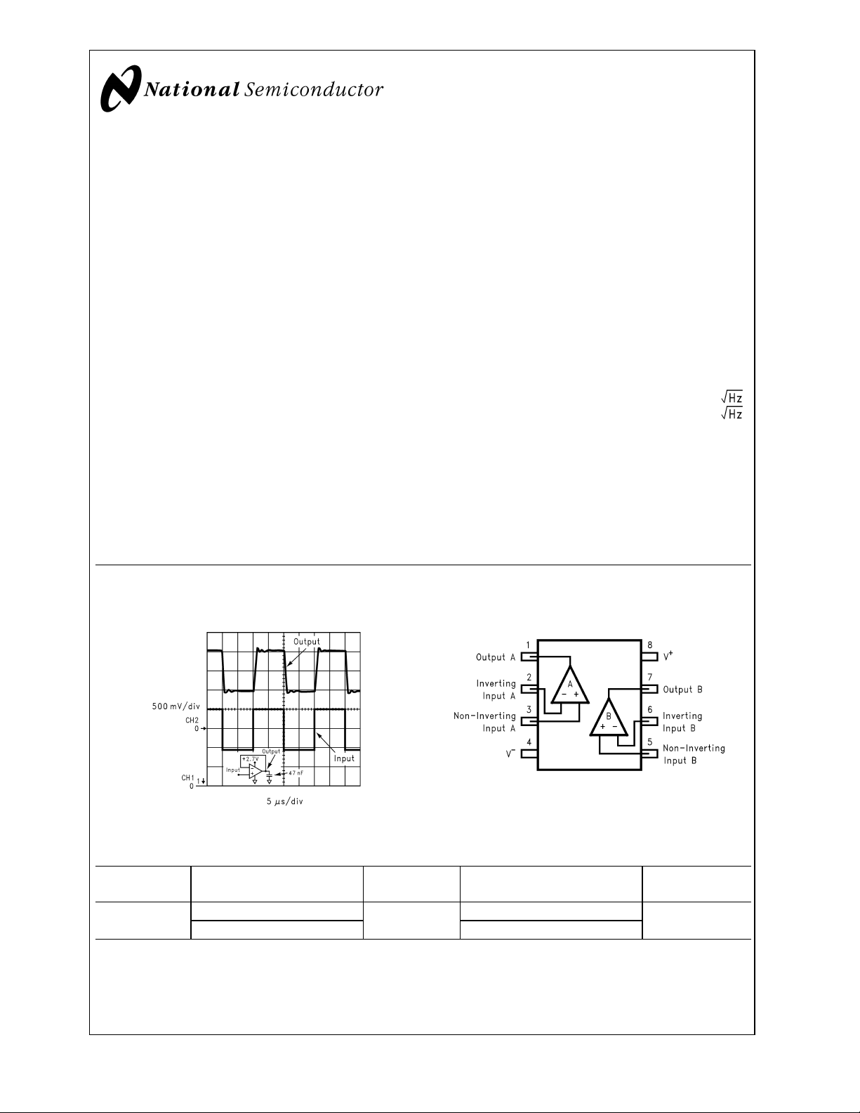
Output Response with Heavy Capacitive Load
driver applications
COM
Features
(VS=5V,TA= 25˚C, Typical values unless specified).
n GBWP 21MHz
n Wide supply voltage range 2.5V to 22V
n Slew rate 12V/µs
n Supply current/channel 1.15 mA
n Cap load limit Unlimited
n Output short circuit current +53mA/−75mA
n +/−5% Settling time 400ns (500pF, 100mV
n Input common mode voltage 0.3V beyond rails
n Input voltage noise 15nV/
n Input current noise 1pA/
n THD+N
PP
<
step)
0.05%
Applications
n TFT-LCD flat panel V
n A/D converter buffer
n High side/low side sensing
n Headphone amplifier
Connection Diagram
driver
COM
8-Pin MSOP
Top View
20021037
20021001
Ordering Information
Package Part Number Package
Marking
8-Pin MSOP LM8262MM
LM8262MMX 3.5k Units Tape and Reel
© 2002 National Semiconductor Corporation DS200210 www.national.com
A46
Media Transport NSC Drawing
1k Units Tape and Reel
MUA08A
Page 2
Absolute Maximum Ratings (Note 1)
If Military/Aerospace specified devices are required,
LM8262
please contact the National Semiconductor Sales Office/
Distributors for availability and specifications.
ESD Tolerance
Differential +/−10V
V
IN
Output Short Circuit Duration (Notes 3, 11)
Supply Voltage (V
+-V−
) 24V
Voltage at Input/Output pins V
2KV (Note 2)
200V(Note 9)
+
+0.8V, V−−0.8V
Soldering Information:
Infrared or Convection (20 sec.) 235˚C
Wave Soldering (10 sec.) 260˚C
Operating Ratings
Supply Voltage (V+-V−) 2.5V to 22V
Junction Temperature Range(Note 4) −40˚C to +85˚C
Package Thermal Resistance, θ
8-Pin MSOP 235˚C/W
Storage Temperature Range −65˚C to +150˚C
Junction Temperature (Note 4) +150˚C
2.7V Electrical Characteristics
Unless otherwise specified, all limits guaranteed for TJ= 25˚C, V+= 2.7V, V−= 0V, VCM= 0.5V, VO=V+/2, and
>
1MΩ to V−. Boldface limits apply at the temperature extremes.
R
L
Symbol Parameter Condition
V
OS
TC V
Input Offset Voltage VCM= 0.5V & VCM= 2.2V – +/−0.7 +/−5
Input Offset Average Drift VCM= 0.5V & VCM= 2.2V
OS
(Note 12)
I
B
Input Bias Current VCM= 0.5V
(Note 7)
VCM= 2.2V
(Note 7)
I
OS
CMRR Common Mode Rejection
Input Offset Current VCM= 0.5V & VCM= 2.2V – 20 250
VCMstepped from 0V to 1.0V 76
Ratio
stepped from 1.7V to 2.7V – 100 –
CM
V
stepped from 0V to 2.7V 58
CM
+
+PSRR Positive Power Supply
= 2.7V to 5V 78
V
Rejection Ratio
CMVR Input Common-Mode Voltage
CMRR>50dB – −0.3 −0.1
Range
A
VOL
V
O
Large Signal Voltage Gain VO= 0.5 to 2.2V,
−
−
−
Output Swing
= 10k to V
R
L
= 0.5 to 2.2V,
V
O
=2ktoV
R
L
RL= 10k to V
High
−
−
Output Swing
RL=2ktoV
= 10k to V
R
L
Low
I
SC
Output Short Circuit Current Sourcing to V
−
VID= 200mV (Note 10)
Sinking to V
+
VID= −200mV (Note 10)
Min
(Note 6)
– +/−2 – µV/C
– −1.20 −2.00
– +0.49 +1.00
60
50
74
2.8
2.7
70
67
67
63
2.49
2.46
2.45
2.41
– 90 100
30
20
50
30
Typ
(Note 5)
100 –
70 –
104 – dB
3.0 – V
78 – dB
73 – dB
2.59 –
2.53 –
48 –
65 –
,(Note 4)
JA
Max
(Note 6)
+/−7
−2.70
+1.60
400
0.0
120
Units
mV
µA
nA
dBV
V
V
mV
mA
www.national.com 2
Page 3
2.7V Electrical Characteristics (Continued)
Unless otherwise specified, all limits guaranteed for TJ= 25˚C, V+= 2.7V, V−= 0V, VCM= 0.5V, VO=V+/2, and
>
1MΩ to V−. Boldface limits apply at the temperature extremes.
R
L
Symbol Parameter Condition
I
S
SR Slew Rate (Note 8) AV= +1,VI=2V
f
u
Supply Current (both amps) No load, VCM= 0.5V – 2.0 2.5
PP
Unity Gain-Frequency VI= 10mV, RL=2kΩ to V+/2 – 10 – MHz
Min
(Note 6)
– 9 – V/µs
GBWP Gain Bandwidth Product f = 50KHz 15.5
14
Phi
e
n
m
Phase Margin VI= 10mV – 50 – Deg
Input-Referred Voltage Noise f = 2KHz, RS=50Ω – 15 – nV/
Typ
(Note 5)
21 – MHz
Max
(Note 6)
3.0
LM8262
Units
mA
i
n
f
max
Input-Referred Current Noise f = 2KHz – 1 – pA/
Full Power Bandwidth ZL= (20pF || 10kΩ)toV+/2 – 1 – MHz
5V Electrical Characteristics
Unless otherwise specified, all limited guaranteed for TJ= 25˚C, V+= 5V, V−= 0V, VCM= 1V, VO=V+/2, and
>
1MΩ to V−. Boldface limits apply at the temperature extremes.
R
L
Symbol Parameter Condition
V
OS
TC V
Input Offset Voltage VCM=1V&VCM= 4.5V – +/−0.7 +/−5
Input Offset Average Drift VCM=1V&VCM= 4.5V
OS
(Note 12)
I
B
Input Bias Current VCM=1V
(Note 7)
= 4.5V
V
CM
(Note 7)
I
OS
CMRR Common Mode Rejection
Input Offset Current VCM=1V&VCM= 4.5V – 20 250
VCMstepped from 0V to 3.3V 84
Ratio
stepped from 4V to 5V – 100 –
CM
V
stepped from 0V to 5V 64
CM
+PSRR Positive Power Supply
V+= 2.7V to 5V, VCM= 0.5V 78
Rejection Ratio
>
CMVR Input Common-Mode Voltage
CMRR
50dB – −0.3 −0.1
Range
A
VOL
V
O
Large Signal Voltage Gain VO= 0.5 to 4.5V,
−
−
−
Output Swing
= 10k to V
R
L
= 0.5 to 4.5V,
V
O
=2ktoV
R
L
RL= 10k to V
High
−
−
Output Swing
=2ktoV
R
L
= 10k to V
R
L
Low
Min
(Note 6)
– +/−2 – µV/˚C
– −1.18 −2.00
– +0.49 +1.00
72
61
74
5.1
5.0
74
70
70
66
4.75
4.72
4.70
4.66
– 86 125
Typ
(Note 5)
110 –
80 –
104 – dB
5.3 – V
84 –
80 –
4.87 –
4.81 –
Max
(Note 6)
+/− 7
−2.70
+1.60
400
0.0
135
Units
mV
µA
nA
dBV
V
dB
V
mV
www.national.com3
Page 4

5V Electrical Characteristics (Continued)
Unless otherwise specified, all limited guaranteed for TJ= 25˚C, V+= 5V, V−= 0V, VCM= 1V, VO=V+/2, and
LM8262
>
1MΩ to V−. Boldface limits apply at the temperature extremes.
R
L
Symbol Parameter Condition
I
SC
Output Short Circuit Current Sourcing to V
−
VID= 200mV (Note 10)
Sinking to V
+
VID= −200mV (Note 10)
I
S
SR Slew Rate (Note 8) AV= +1, VI=5V
f
u
Supply Current (both amps) No load, VCM= 1V – 2.3 2.8
PP
Unity Gain Frequency VI= 10mV,
=2kΩ to V+/2
R
L
Min
(Note 6)
35
20
60
50
10
GBWP Gain-Bandwidth Product f = 50KHz 16
15
Phi
e
m
n
Phase Margin VI= 10mV – 53 – Deg
Input-Referred Voltage Noise f = 2KHz, RS=50Ω – 15 – nV/
Typ
(Note 5)
7
– 10.5 – MHz
Max
(Note 6)
Units
53 –
75 –
mA
mA
3.5
12 – V/µs
21 – MHz
i
n
f
max
t
S
THD+N Total Harmonic Distortion +
Input-Referred Current Noise f = 2KHz – 1 – pA/
Full Power Bandwidth ZL= (20pF || 10kΩ)toV+/2 – 900 – KHz
Settling Time (+/−5%) 100mVPPStep, 500pF load – 400 – ns
Noise
R
=1kΩ to V+/2
L
f = 10KHz to A
= +2, 4VPPswing
V
– 0.05 – %
+/−11V Electrical Characteristics
Unless otherwise specified, all limited guaranteed for TJ= 25˚C, V+= 11V, V−= −11V, VCM= 0V, VO= 0V, and
>
1MΩ to 0V. Boldface limits apply at the temperature extremes.
R
L
Symbol Parameter Condition
V
OS
TC V
Input Offset Voltage VCM= −10.5V & VCM= 10.5V – +/−0.7 +/−7
Input Offset Average Drift VCM= −10.5V & VCM= 10.5V
OS
(Note 12)
I
B
Input Bias Current VCM= −10.5V
(Note 7)
= 10.5V
V
CM
(Note 7)
I
OS
CMRR Common Mode Rejection
Input Offset Current VCM= −10.5V & VCM= 10.5V – 30 275
stepped from −11V to 9V 84
V
CM
Ratio
V
stepped from −11V to 11V 74
CM
+PSRR Positive Power Supply
V+= 9V to 11V 70
Rejection Ratio
−
−PSRR Negative Power Supply
= −9V to −11V 70
V
Rejection Ratio
Min
(Note 6)
– +/−2 – µV/˚C
– −1.05 −2.00
– +0.49 +1.00
80
72
66
66
Typ
(Note 5)
(Note 6)
100 –
88 –
100 – dB
100 – dB
Max
+/− 9
−2.80
+1.50
550
Units
mV
µA
nA
dBVCMstepped from 10V to 11V – 100 –
www.national.com 4
Page 5

+/−11V Electrical Characteristics (Continued)
Unless otherwise specified, all limited guaranteed for TJ= 25˚C, V+= 11V, V−= −11V, VCM= 0V, VO= 0V, and
>
1MΩ to 0V. Boldface limits apply at the temperature extremes.
R
L
Symbol Parameter Condition
>
CMVR Input Common-Mode Voltage
CMRR
50dB – −11.3 −11.1
Min
(Note 6)
Range
11.1
11.0
A
VOL
V
O
Large Signal Voltage Gain VO= 0V to +/−9V,
= 10kΩ
R
L
V
= 0V to +/−9V,
O
=2kΩ
R
L
Output Swing
RL= 10kΩ 10.65
High
=2kΩ 10.6
R
L
78
74
72
66
10.61
10.55
Output Swing
RL= 10kΩ – −10.98 −10.75
Low
=2kΩ – −10.91 −10.65
R
L
I
SC
I
S
Output Short Circuit Current Sourcing to ground
Supply Current No load, VCM= 0V – 2.5 4
SR Slew Rate
= 200mV (Note 10)
V
ID
Sinking to ground
= 200mV (Note 10)
V
ID
= +1, VI= 16V
A
V
PP
40
25
65
55
10
(Note 8)
f
U
Unity Gain Frequency VI= 10mV, RL=2kΩ – 13 – MHz
GBWP Gain-Bandwidth Product f = 50KHz 18
16
Phi
e
n
m
Phase Margin VI= 10mV – 58 – Deg
Input-Referred Voltage Noise f = 2KHz, RS=50Ω – 15 – nV/
8
Typ
(Note 5)
(Note 6)
11.3 – V
85 –
79 –
10.77 –
10.69 –
60 –
100 –
15 – V/µs
24 – MHz
Max
−11.0
−10.65
−10.6
5
LM8262
Units
V
dB
V
V
mA
mA
i
n
t
S
Input-Referred Current Noise f = 2KHz – 1 – pA/
Settling Time (+/−1%, AV=
+1)
THD+N Total Harmonic Distortion
+Noise
CT
REJ
Cross-Talk Rejection f = 5MHz, Driver
Positive Step, 5V
Negative Step, 5V
R
=1kΩ, f = 10KHz,
L
= +2, 15VPPswing
A
V
= 10kΩ
R
L
PP
PP
– 320 –
– 600 –
ns
– 0.01 – %
–68–dB
www.national.com5
Page 6

+/−11V Electrical Characteristics (Continued)
Note 1: Absolute Maximum Ratings indicate limits beyond which damage to the device may occur. Operating Rating indicate conditions for which the device is
LM8262
intended to be functional, but specific performance is not guaranteed. For guaranteed specifications and the test conditions, see the Electrical Characteristics.
Note 2: Human body model, 1.5kΩ in series with 100pF.
Note 3: Applies to both single-supply and split-supply operation. Continuous short circuit operation at elevated ambient temperature can result in exceeding the
maximum allowed junction temperature of 150˚C.
Note 4: The maximum power dissipation is a function of T
P
=(TJ(max) - TA)/ θJA. All numbers apply for packages soldered directly onto a PC board.
D
Note 5: Typical Values represent the most likely parametric norm.
Note 6: All limits are guaranteed by testing or statistical analysis.
Note 7: Positive current corresponds to current flowing into the device.
Note 8: Slew rate is the slower of the rising and falling slew rates. Connected as a Voltage Follower.
Note 9: Machine Model, 0Ω is series with 200pF.
Note 10: Short circuit test is a momentary test. See Note 11.
Note 11: Output short circuit duration is infinite for V
Note 12: Offset voltage average drift determined by dividing the change in V
(max), θJA, and TA. The maximum allowable power dissipation at any ambient temperature is
J
≤ 6V at room temperature and below. For V
S
at temperature extremes into the total temperature change.
OS
>
6V, allowable short circuit duration is 1.5ms.
S
Typical Performance Characteristics T
vs. VCMfor 3 Representative Units VOSvs. VCMfor 3 Representative Units
V
OS
20021030 20021029
VOSvs. VCMfor 3 Representative Units VOSvs. VSfor 3 Representative Units
= 25˚C, Unless Otherwise Noted
A
20021031
www.national.com 6
20021034
Page 7

LM8262
Typical Performance Characteristics T
vs. VSfor 3 Representative Units VOSvs. VSfor 3 Representative Units
V
OS
20021035 20021033
IBvs. V
CM
= 25˚C, Unless Otherwise Noted (Continued)
A
IBvs. V
S
ISvs. V
CM
20021024
ISvs. V
20021027 20021028
CM
20021036
www.national.com7
Page 8

Typical Performance Characteristics T
LM8262
I
vs. V
S
CM
ISvs. VS(NPN side) Gain/Phase vs. Frequency
= 25˚C, Unless Otherwise Noted (Continued)
A
ISvs. VS(PNP side)
20021068 20021025
20021026
Unity Gain Frequency vs. V
S
20021007 20021008
www.national.com 8
Phase Margin vs. V
20021018
S
Page 9

LM8262
Typical Performance Characteristics T
Unity Gain Freq. and Phase Margin vs. V
S
20021004
= 25˚C, Unless Otherwise Noted (Continued)
A
www.national.com9
Page 10

Physical Dimensions inches (millimeters)
unless otherwise noted
8-Pin MSOP
NS Package Number MUA08A
LIFE SUPPORT POLICY
NATIONAL’S PRODUCTS ARE NOT AUTHORIZED FOR USE AS CRITICAL COMPONENTS IN LIFE SUPPORT
DEVICES OR SYSTEMS WITHOUT THE EXPRESS WRITTEN APPROVAL OF THE PRESIDENT AND GENERAL
COUNSEL OF NATIONAL SEMICONDUCTOR CORPORATION. As used herein:
1. Life support devices or systems are devices or
systems which, (a) are intended for surgical implant
LM8262 Dual RRIO, High Output Current & Unlimited Cap Load Op Amp in MSOP
into the body, or (b) support or sustain life, and
whose failure to perform when properly used in
accordance with instructions for use provided in the
2. A critical component is any component of a life
support device or system whose failure to perform
can be reasonably expected to cause the failure of
the life support device or system, or to affect its
safety or effectiveness.
labeling, can be reasonably expected to result in a
significant injury to the user.
National Semiconductor
Corporation
Americas
Email: support@nsc.com
www.national.com
National Semiconductor
Europe
Fax: +49 (0) 180-530 85 86
Email: europe.support@nsc.com
Deutsch Tel: +49 (0) 69 9508 6208
English Tel: +44 (0) 870 24 0 2171
Français Tel: +33 (0) 1 41 91 8790
National Semiconductor
Asia Pacific Customer
Response Group
Tel: 65-2544466
Fax: 65-2504466
Email: ap.support@nsc.com
National Semiconductor
Japan Ltd.
Tel: 81-3-5639-7560
Fax: 81-3-5639-7507
National does not assume any responsibility for use of any circuitry described, no circuit patent licenses are implied and National reserves the right at any time without notice to change said circuitry and specifications.
 Loading...