

Page 1
LM8261 Single
RRIO, High Output Current & Unlimited Cap Load Op
Amp in SOT23-5
General Description
The LM8261 is a Rail-to-Rail input and output Op Amp which
can operate with a wide supply voltage range. This device
has high output current drive, greater than Rail-to-Rail input
common mode voltage range, unlimited capacitive load drive
capability, and provides tested and guaranteed high speed
and slew rate while requiring only 0.97mA supply current. It
is specifically designed to handle the requirements of flat
panel TFT panel V
suitable for other low power, and medium speed applications
which require ease of use and enhanced performance over
existing devices.
Greater than Rail-to-Rail input common mode voltage range
with 50dB of Common Mode Rejection, allows high side and
low side sensing, among many applications, without having
any concerns over exceeding the range and no compromise
in accuracy. Exceptionally wide operating supply voltage
range of 2.5V to 30V alleviates any concerns over functionality under extreme conditions and offers flexibility of use in
multitude of applications. In addition, most device parameters are insensitive to power supply variations; this design
enhancement is yet another step in simplifying its usage.
The output stage has low distortion (0.05% THD+N) and can
supply a respectable amount of current (15mA) with minimal
headroom from either rail (300mV).
driver applications as well as being
COM
The LM8261 is offered in the space saving SOT23-5 package.
Features
(VS=5V,TA= 25˚C, Typical values unless specified).
n GBWP 21MHz
n Wide supply voltage range 2.5V to 30V
n Slew rate 12V/µs
n Supply current 0.97 mA
n Cap load limit Unlimited
n Output short circuit current +53mA/−75mA
±
n
5% Settling time 400ns (500pF, 100mVPPstep)
n Input common mode voltage 0.3V beyond rails
n Input voltage noise 15nV/
n Input current noise 1pA/
n THD+N
Applications
n TFT-LCD flat panel V
n A/D converter buffer
n High side/low side sensing
n Headphone amplifier
COM
driver
April 2006
<
0.05%
LM8261 Single RRIO, High Output Current & Unlimited Cap Load Op Amp in SOT23-5
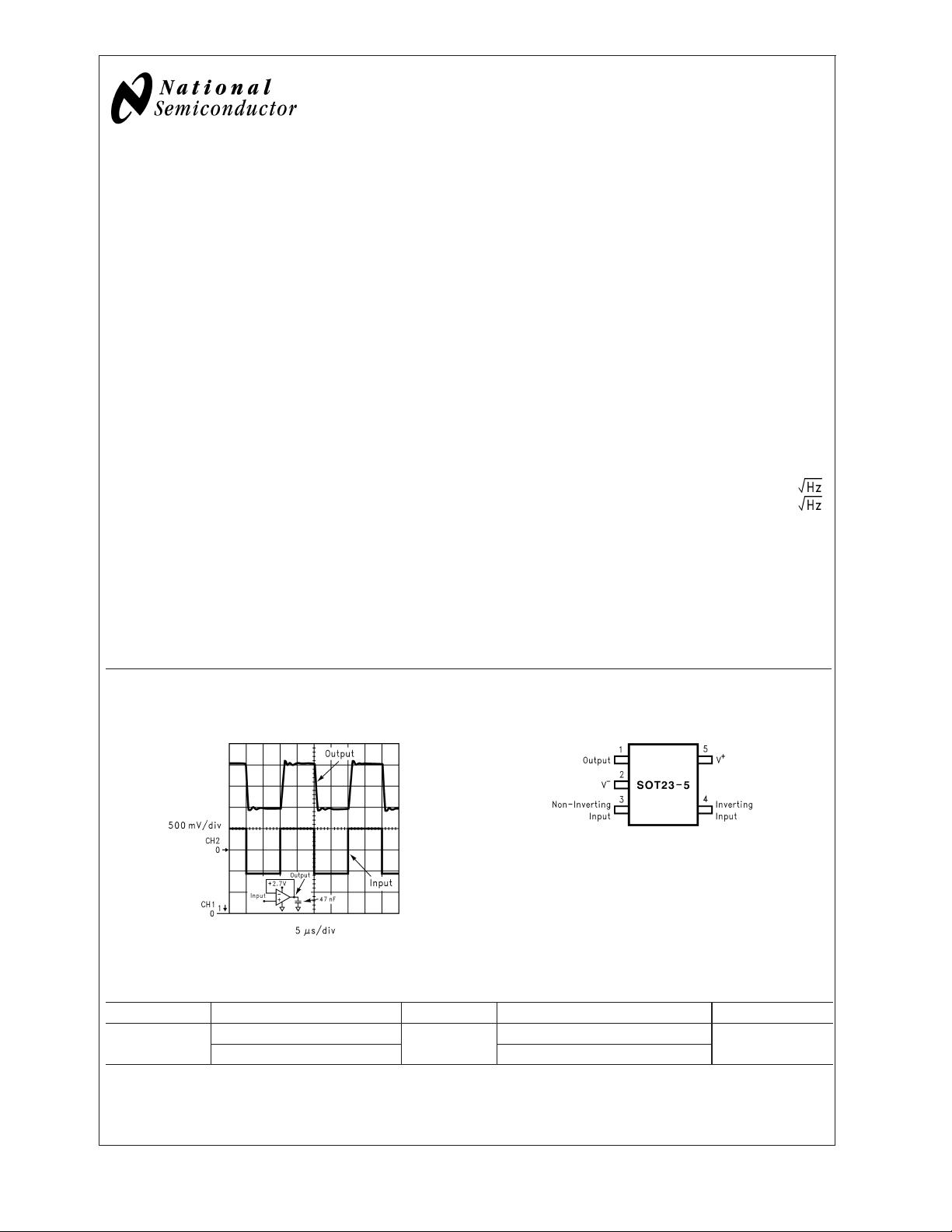
Output Response with Heavy Capacitive Load
10108437
Connection Diagram
SOT23-5
10108462
Top View
Ordering Information
Package Ordering Info Pkg Marking Supplied As NSC Drawing
5-Pin SOT-23
LM8261M5
LM8261M5X 3k Units Tape and Reel
A45A
1k Units Tape and Reel
MF05A
© 2006 National Semiconductor Corporation DS101084 www.national.com
Page 2
Absolute Maximum Ratings (Note 1)
If Military/Aerospace specified devices are required,
LM8261
please contact the National Semiconductor Sales Office/
Distributors for availability and specifications.
Junction Temperature (Note 4) +150˚C
Soldering Information:
Infrared or Convection (20 sec.) 235˚C
Wave Soldering (10 sec.) 260˚C
ESD Tolerance
Human Body Model 2KV (Note 2)
Operating Ratings
Machine Model 200V(Note 9)
Differential +/−10V
V
IN
Output Short Circuit Duration (Notes 3, 11)
Supply Voltage (V
Voltage at Input/Output pins V
+-V−
) 32V
+
+0.8V, V−−0.1V
Supply Voltage (V+-V−) 2.5V to 30V
Temperature Range(Note 4) −40˚C to +85˚C
Package Thermal Resistance, θ
SOT23-5 325˚C/W
Storage Temperature Range −65˚C to +150˚C
2.7V Electrical Characteristics (Note 13)
Unless otherwise specified, all limits guaranteed for TA= 25˚C, V+= 2.7V, V−= 0V, VCM= 0.5V, VO=V+/2, and
>
1MΩ to V−. Boldface limits apply at the temperature extremes.
R
L
Symbol Parameter Condition
V
OS
TC V
Input Offset Voltage VCM=0.5V&VCM= 2.2V +/−0.7 +/−5
Input Offset Average Drift VCM=0.5V&VCM= 2.2V
OS
(Note 12)
I
B
Input Bias Current VCM= 0.5V
(Note 7)
VCM= 2.2V
(Note 7)
I
OS
Input Offset Current VCM=0.5V&VCM= 2.2V 20 250
CMRR Common Mode Rejection Ratio VCMstepped from 0V to 1.0V 100 76
stepped from 1.7V to 2.7V 100
V
CM
V
stepped from 0V to 2.7V 70 58
CM
+
+PSRR Positive Power Supply Rejection
= 2.7V to 5V 104 78
V
Ratio
CMVR Input Common-Mode Voltage
CMRR>50dB −0.3 −0.1
Range
A
VOL
V
O
Large Signal Voltage Gain VO= 0.5 to 2.2V,
−
−
−
Output Swing
= 10K to V
R
L
= 0.5 to 2.2V,
V
O
=2KtoV
R
L
RL= 10K to V
High
−
−
Output Swing
=2KtoV
R
L
= 10K to V
R
L
Low
I
SC
Output Short Circuit Current Sourcing to V
−
VID= 200mV (Note 10)
Sinking to V
+
VID= −200mV (Note 10)
Typ
(Note 5)
+/−2 – µV/C
−1.20 −2.00
+0.49 +1.00
3.0 2.8
78 70
73 67
2.59 2.49
2.53 2.45
90 100
48 30
65 50
,(Note 4)
JA
Limit
(Note 6)
+/−7
−2.70
+1.60
400
60
50
74
0.0
2.7
67
63
2.46
2.41
120
20
30
Units
mV
max
µA
max
nA
max
dB
min
dB
min
V
max
V
min
dB
min
dB
min
V
min
mV
max
mA
min
mA
min
www.national.com 2
Page 3
2.7V Electrical Characteristics (Note 13) (Continued)
Unless otherwise specified, all limits guaranteed for TA= 25˚C, V+= 2.7V, V−= 0V, VCM= 0.5V, VO=V+/2, and
>
1MΩ to V−. Boldface limits apply at the temperature extremes.
R
L
Symbol Parameter Condition
I
S
SR Slew Rate (Note 8) AV= +1,VI=2V
f
u
Supply Current No load, VCM= 0.5V 0.95 1.20
PP
Unity Gain-Frequency VI= 10mV, RL=2KΩ to V+/2 10 – MHz
Typ
(Note 5)
9 – V/µs
GBWP Gain Bandwidth Product f = 50KHz 21 15.5
Phi
e
m
n
Phase Margin VI= 10mV 50 – Deg
Input-Referred Voltage Noise f = 2KHz, RS=50Ω 15 – nV/
Limit
(Note 6)
1.50
14
LM8261
Units
mA
max
MHz
min
i
f
n
MAX
Input-Referred Current Noise f = 2KHz 1 pA/
Full Power Bandwidth ZL= (20pF || 10KΩ)toV+/2 1 – MHz
5V Electrical Characteristics (Note 13)
Unless otherwise specified, all limited guaranteed for TA= 25˚C, V+= 5V, V−= 0V, VCM= 1V, VO=V+/2, and
>
1MΩ to V−. Boldface limits apply at the temperature extremes.
R
L
Symbol Parameter Condition
V
OS
TC V
Input Offset Voltage VCM=1V&VCM= 4.5V +/−0.7 +/−5
Input Offset Average Drift VCM=1V&VCM= 4.5V
OS
Typ
(Note 5)
+/−2 – µV/˚C
(Note 12)
I
B
Input Bias Current VCM=1V
−1.18 −2.00
(Note 7)
= 4.5V
V
CM
+0.49 +1.00
(Note 7)
I
OS
Input Offset Current VCM=1V&VCM= 4.5V 20 250
CMRR Common Mode Rejection Ratio VCMstepped from 0V to 3.3V 110 84
stepped from 4V to 5V 100 –
V
CM
V
stepped from 0V to 5V 80 64
CM
+PSRR Positive Power Supply Rejection Ratio V+= 2.7V to 5V, VCM= 0.5V 104 78
>
CMVR Input Common-Mode Voltage Range CMRR
50dB −0.3 −0.1
5.3 5.1
A
VOL
V
O
Large Signal Voltage Gain VO= 0.5 to 4.5V,
−
−
−
Output Swing
= 10K to V
R
L
= 0.5 to 4.5V,
V
O
=2KtoV
R
L
RL= 10K to V
84 74
80 70
4.87 4.75
High
−
−
4.81 4.70
86 125
Output Swing
=2KtoV
R
L
= 10K to V
R
L
Low
Limit
(Note 6)
+/− 7
−2.70
+1.60
400
72
61
74
0.0
5.0
70
66
4.72
4.66
135
Units
mV
max
µA
max
nA
max
dB
min
dB
min
V
max
V
min
dB
min
V
min
mV
max
www.national.com3
Page 4
5V Electrical Characteristics (Note 13) (Continued)
Unless otherwise specified, all limited guaranteed for TA= 25˚C, V+= 5V, V−= 0V, VCM= 1V, VO=V+/2, and
LM8261
>
1MΩ to V−. Boldface limits apply at the temperature extremes.
R
L
Symbol Parameter Condition
I
SC
Output Short Circuit Current Sourcing to V
−
Typ
(Note 5)
53 35
VID= 200mV (Note 10)
Sinking to V
+
75 60
VID= −200mV (Note 10)
I
S
SR Slew Rate (Note 8) AV= +1, VI=5V
f
u
Supply Current No load, VCM= 1V 0.97 1.25
12 10
10.5 – MHz
Unity Gain Frequency VI= 10mV,
=2KΩ to V+/2
R
L
PP
GBWP Gain-Bandwidth Product f = 50KHz 21 16
Phi
e
m
n
Phase Margin VI= 10mV 53 – Deg
Input-Referred Voltage Noise f = 2KHz, RS=50Ω 15 – nV/
Limit
(Note 6)
20
50
1.75
7
15
Units
mA
min
mA
max
V/µs
min
MHz
min
i
n
f
MAX
t
S
THD+N Total Harmonic Distortion + Noise R
±
Input-Referred Current Noise f = 2KHz 1 – pA/
Full Power Bandwidth ZL= (20pF || 10kΩ)toV+/2 900 – KHz
Settling Time (±5%) 100mVPPStep, 500pF load 400 – ns
=1KΩ to V+/2
L
f = 10KHz to A
= +2, 4VPPswing
V
0.05 – %
15V Electrical Characteristics (Note 13)
Unless otherwise specified, all limited guaranteed for TA= 25˚C, V+= 15V, V−= −15V, VCM= 0V, VO= 0V, and
>
1MΩ to 0V. Boldface limits apply at the temperature extremes.
R
L
Symbol Parameter Condition
V
OS
Input Offset Voltage VCM= −14.5V & VCM= 14.5V +/−0.7 +/−7
Typ
(Note 5)
Limit
(Note 6)
+/− 9
TC V
Input Offset Average Drift VCM= −14.5V & VCM= 14.5V
OS
+/−2 – µV/˚C
(Note 12)
I
B
I
OS
Input Bias Current VCM= −14.5V
(Note 7)
= 14.5V
V
CM
(Note 7)
−1.05 −2.00
−2.80
+0.49 +1.00
+1.50
Input Offset Current VCM= −14.5V & VCM= 14.5V 30 275
550
CMRR Common Mode Rejection Ratio V
stepped from −15V to 13V 100 84
CM
80
VCMstepped from 14V to 15V 100 –
V
stepped from −15V to 15V 88 74
CM
72
+PSRR Positive Power Supply Rejection Ratio V+= 12V to 15V 100 70
66
−
−PSRR Negative Power Supply Rejection
Ratio
= −12V to −15V 100 70
V
66
Units
mV
max
µA
max
nA
max
dB
min
dB
min
dB
min
www.national.com 4
Page 5
±
15V Electrical Characteristics (Note 13) (Continued)
Unless otherwise specified, all limited guaranteed for TA= 25˚C, V+= 15V, V−= −15V, VCM= 0V, VO= 0V, and
>
1MΩ to 0V. Boldface limits apply at the temperature extremes.
R
L
Symbol Parameter Condition
>
CMVR Input Common-Mode Voltage Range CMRR
50dB −15.3 −15.1
Typ
(Note 5)
Limit
(Note 6)
−15.0
15.3 15.1
15.0
A
VOL
V
O
Large Signal Voltage Gain VO=0Vto±13V,
= 10KΩ
R
L
V
=0Vto±13V,
O
=2KΩ
R
L
Output Swing
RL= 10KΩ 14.83 14.65
High
=2KΩ 14.73 14.60
R
L
85 78
74
79 72
66
14.61
14.55
Output Swing
Low
RL= 10KΩ −14.91 −14.75
−14.65
=2KΩ −14.83 −14.65
R
L
−14.60
I
SC
Output Short Circuit Current Sourcing to ground
= 200mV (Note 10)
V
ID
Sinking to ground
= 200mV (Note 10)
V
ID
I
S
Supply Current No load, VCM= 0V 1.30 1.50
60 40
25
100 70
60
1.90
SR Slew Rate
= +1, VI= 24V
A
V
PP
15 10
(Note 8)
f
u
Unity Gain Frequency VI= 10mV, RL=2KΩ 14 – MHz
GBWP Gain-Bandwidth Product f = 50KHz 24 18
16
Phi
e
n
m
Phase Margin VI= 10mV 58 – Deg
Input-Referred Voltage Noise f = 2KHz, RS=50Ω 15 – nV/
LM8261
Units
V
max
V
min
dB
min
V
min
V
max
mA
min
mA
max
V/µs
8
min
MHz
min
i
n
f
MAX
t
s
THD+N Total Harmonic Distortion +Noise R
Note 1: Absolute Maximum Ratings indicate limits beyond which damage to the device may occur. Operating Rating indicate conditions for which the device is
intended to be functional, but specific performance is not guaranteed. For guaranteed specifications and the test conditions, see the Electrical Characteristics.
Note 2: Human Body Model is 1.5kΩ in series with 100pF.
Note 3: Applies to both single-supply and split-supply operation. Continuous short circuit operation at elevated ambient temperature can result in exceeding the
maximum allowed junction temperature of 150˚C.
Note 4: The maximum power dissipation is a function of T
P
D
Note 5: Typical Values represent the most likely parametric norm.
Note 6: All limits are guaranteed by testing or statistical analysis.
Note 7: Positive current corresponds to current flowing into the device.
Note 8: Slew rate is the slower of the rising and falling slew rates. Connected as a Voltage Follower.
Note 9: Machine Model, 0Ω is series with 200pF.
Note 10: Short circuit test is a momentary test. See Note 11.
Note 11: Output short circuit duration is infinite for V
Input-Referred Current Noise f = 2KHz 1 – pA/
Full Power Bandwidth ZL= 20pF || 10KΩ 160 – KHz
Settling Time (±1%, AV= +1) Positive Step, 5V
Negative Step, 5V
L
A
V
=(T
J(MAX)-TA
)/ θJA. All numbers apply for packages soldered directly onto a PC board.
J(max)
≤ 6V at room temperature and below. For V
S
PP
PP
=1KΩ, f = 10KHz,
= +2, 28VPPswing
, θJA, and TA. The maximum allowable power dissipation at any ambient temperature is
>
6V, allowable short circuit duration is 1.5ms.
S
320 –
600 –
0.01 – %
www.national.com5
ns
Page 6
±
15V Electrical Characteristics (Note 13) (Continued)
Note 12: Offset voltage average drift determined by dividing the change in VOSat temperature extremes into the total temperature change.
LM8261
Note 13: Electrical Table values apply only for factory testing conditions at the temperature indicated. Factory testing conditions result in very limited self-heating
of the device such that T
. No guarantee of parametric performance is indicated in the electrical tables under conditions of internal self heating where T
J=TA
Typical Performance Characteristics
TA= 25˚C, Unless Otherwise Noted
vs. VCMfor 3 Representative Units VOSvs. VCMfor 3 Representative Units
V
OS
>
TA.
J
10108430
VOSvs. VCMfor 3 Representative Units VOSvs. VSfor 3 Representative Units
10108431 10108434
10108429
www.national.com 6
Page 7
LM8261
Typical Performance Characteristics T
V
vs. VSfor 3 Representative Units VOSvs. VSfor 3 Representative Units
OS
10108435
IBvs. V
CM
= 25˚C, Unless Otherwise Noted (Continued)
A
IBvs. V
S
10108433
ISvs. V
CM
10108424 10108436
ISvs. V
CM
10108427 10108428
www.national.com7
Page 8

Typical Performance Characteristics T
LM8261
I
S
vs. V
CM
= 25˚C, Unless Otherwise Noted (Continued)
A
ISvs. VS(PNP side)
10108468
ISvs. VS(NPN side) Gain/Phase vs. Frequency
10108426
Unity Gain Frequency vs. V
S
Phase Margin vs. V
10108425
10108418
S
10108407 10108408
www.national.com 8
Page 9

LM8261
Typical Performance Characteristics T
Unity Gain Freq. and Phase Margin vs. V
Phase Margin vs. Load Unity Gain Freq. and Phase Margin vs. C
S
10108404
= 25˚C, Unless Otherwise Noted (Continued)
A
Unity Gain Frequency vs. Load
10108405
L
10108406
CMRR vs. Frequency +PSRR vs. Frequency
10108414 10108416
10108409
www.national.com9
Page 10

Typical Performance Characteristics T
LM8261
−PSRR vs. Frequency Output Voltage vs. Output Sourcing Current
= 25˚C, Unless Otherwise Noted (Continued)
A
10108417
10108446
Output Voltage vs. Output Sourcing Current Output Voltage vs. Output Sinking Current
10108444 10108445
Max Output Swing vs. Load Max Output Swing vs. Frequency
10108410
www.national.com 10
10108411
Page 11

LM8261
Typical Performance Characteristics T
% Overshoot vs. Cap Load
10108448 10108447
+SR vs. Cap Load −SR vs. Cap Load
= 25˚C, Unless Otherwise Noted (Continued)
A
±
5% Settling Time vs. Cap Load
10108451 10108452
+SR vs. Cap Load −SR vs. Cap Load
10108449 10108450
www.national.com11
Page 12

Typical Performance Characteristics T
LM8261
Settling Time vs. Error Voltage Settling Time vs. Error Voltage
= 25˚C, Unless Otherwise Noted (Continued)
A
10108443
Input Noise Voltage/Current vs. Frequency Input Noise Voltage for Various V
10108415 10108413
Input Noise Current for Various V
CM
Input Noise Voltage vs. V
CM
10108442
CM
10108412
www.national.com 12
10108455
Page 13

LM8261
Typical Performance Characteristics T
Input Noise Current vs. V
THD+N vs. Frequency THD+N vs. Frequency
CM
10108454
= 25˚C, Unless Otherwise Noted (Continued)
A
THD+N vs. Frequency
10108423
10108422 10108421
THD+N vs. Amplitude THD+N vs. Amplitude
10108419 10108420
www.national.com13
Page 14

Typical Performance Characteristics T
LM8261
Small Signal Step Response Large Signal Step Response
= 25˚C, Unless Otherwise Noted (Continued)
A
10108438
10108440
www.national.com 14
Page 15

Application Hints
BLOCK DIAGRAM AND OPERATIONAL DESCRIPTION
A) Input Stage
LM8261
FIGURE 1. Simplified Schematic Diagram
As can be seen from the simplified schematic in Figure 1, the
input stage consists of two distinct differential pairs (Q1-Q2
and Q3-Q4) in order to accommodate the full Rail-to-Rail
input common mode voltage range. The voltage drop across
R5, R6, R7, and R8 is kept to less than 200mV in order to
allow the input to exceed the supply rails. Q13 acts as a
switch to steer current away from Q3-Q4 and into Q1-Q2, as
the input increases beyond 1.4V of V
+
. This in turn shifts the
signal path from the bottom stage differential pair to the top
one and causes a subsequent increase in the supply current.
In transitioning from one stage to another, certain input stage
parameters (V
OS,Ib,IOS,en
, and in) are determined based
on which differential pair is "on" at the time. Input Bias
current, I
, will change in value and polarity as the input
B
crosses the transition region. In addition, parameters such
as PSRR and CMRR which involve the input offset voltage
will also be effected by changes in V
across the differen-
CM
tial pair transition region.
The input stage is protected with the combination of R9-R10
and D1, D2, D3, and D4 against differential input over-
10108467
voltages. This fault condition could otherwise harm the differential pairs or cause offset voltage shift in case of prolonged over voltage. As shown in Figure 2, if this voltage
reaches approximately
±
1.4V at 25˚C, the diodes turn on
and current flow is limited by the internal series resistors (R9
±
and R10). The Absolute Maximum Rating of
tial on V
still needs to be observed. With temperature
IN
10V differen-
variation, the point were the diodes turn on will change at the
rate of 5mV/˚C.
www.national.com15
Page 16

Application Hints (Continued)
LM8261
FIGURE 2. Input Stage Current vs. Differential Input
Voltage
B) Output Stage
The output stage Figure 1 is comprised of complementary
NPN and PNP common-emitter stages to permit voltage
swing to within a V
the sourcing and Q10 supplies the sinking current load.
Output current limiting is achieved by limiting the V
and Q10; using this approach to current limiting, alleviates
the draw back to the conventional scheme which requires
one V
reduction in output swing.
BE
The frequency compensation circuit includes Miller capacitors from collector to base of each output transistor (see
Figure 1,C
comp9
and C
high frequency gain of the output transistors is high, and the
Miller effect increases the effective value of the capacitors
thereby stabilizing the Op Amp. Large capacitive loads
greatly decrease the high frequency gain of the output transistors thus lowering the effective internal Miller capacitance
- the internal pole frequency increases at the same time a
low frequency pole is created at the Op Amp output due to
the large load capacitor. In this fashion, the internal dominant
pole compensation, which works by reducing the loop gain to
less than 0dB when the phase shift around the feedback
loop is more than 180˚C, varies with the amount of capacitive load and becomes less dominant when the load capacitor has increased enough. Hence the Op Amp is very stable
even at high values of load capacitance resulting in the
uncharacteristic feature of stability under all capacitive loads.
of either supply rail. Q9 supplies
CE(SAT)
). At light capacitive loads, the
comp10
10108466
CE
Output current drive is an important parameter when driving
capacitive loads. This parameter will determine how fast the
output voltage can change. Referring to the Slew Rate vs.
Cap Load Plots (typical performance characteristics section), two distinct regions can be identified. Below about
10,000pF, the output Slew Rate is solely determined by the
Op Amp’s compensation capacitor value and available current into that capacitor. Beyond 10nF, the Slew Rate is
determined by the Op Amp’s available output current. Note
that because of the lower output sourcing current compared
to the sinking one, the Slew Rate limit under heavy capacitive loading is determined by the positive transitions. An
estimate of positive and negative slew rates for loads larger
than 100nF can be made by dividing the short circuit current
value by the capacitor.
For the LM8261, the available output current increases with
the input overdrive. Referring to Figure 3 and Figure 4,
Output Short Circuit Current vs. Input Overdrive, it can be
seen that both sourcing and sinking short circuit current
increase as input overdrive increases. In a closed loop amplifier configuration, during transient conditions while the fed
back output has not quite caught up with the input, there will
be an overdrive imposed on the input allowing more output
current than would normally be available under steady state
condition. Because of this feature, the Op Amp’s output
stage quiescent current can be kept to a minimum, thereby
reducing power consumption, while enabling the device to
deliver large output current when the need arises (such as
during transients).
of Q9
10108457
FIGURE 3. Output Short Circuit Sourcing Current vs.
Input Overdrive
DRIVING CAPACITIVE LOADS
The LM8261 is specifically designed to drive unlimited capacitive loads without oscillations (See Settling Time and
Percent Overshoot vs. Cap Load plots in the typical performance characteristics section). In addition, the output current handling capability of the device allows for good slewing
characteristics even with large capacitive loads (see Slew
Rate vs. Cap Load plots). The combination of these features
is ideal for applications such as TFT flat panel buffers, A/D
converter input amplifiers, etc.
However, as in most Op Amps, addition of a series isolation
resistor between the Op Amp and the capacitive load improves the settling and overshoot performance.
www.national.com 16
Page 17

Application Hints (Continued)
10108456
FIGURE 4. Output Short Circuit Sinking Current vs.
Input Overdrive
Figure 5 shows the output voltage, output current, and the
resulting input overdrive with the device set for A
the input tied to a 1V
step function driving a 47nF capaci-
PP
tor. As can be seen, during the output transition, the input
overdrive reaches 1V peak and is more than enough to
cause the output current to increase to its maximum value
(see Figure 3 and Figure 4 plots). Note that because of the
larger output sinking current compared to the sourcing one,
the output negative transition is faster than the positive one.
=+1and
V
Output Voltage vs. Output Current plot (Typical Performance
Characteristics section) can be used to predict the output
swing. Figure 6 and Figure 7 show this performance along
with several load lines corresponding to loads tied between
the output and ground. In each cases, the intersection of the
device plot at the appropriate temperature with the load line
would be the typical output swing possible for that load. For
example, a 1KΩ load can accommodate an output swing to
within 250mV of V
corresponding to a typical 29.3V
−
and to 330mV of V+(VS=±15V)
unclipped swing.
PP
10108460
FIGURE 6. Output Sourcing Characteristics with Load
Lines
LM8261
10108439
FIGURE 5. Buffer Amplifier scope photo
ESTIMATING THE OUTPUT VOLTAGE SWING
It is important to keep in mind that the steady state output
current will be less than the current available when there is
an input overdrive present. For steady state conditions, the
10108459
FIGURE 7. Output Sinking Characteristics with Load
Lines
www.national.com17
Page 18

Application Hints (Continued)
TFT APPLICATIONS
LM8261
Figure 8 below, shows a typical application where the
LM8261 is used as a buffer amplifier for the V
employed in a TFT LCD flat panel:
COM
signal
10108461
FIGURE 8. V
Driver Application Schematic
COM
Figure 9 shows the time domain response of the amplifier
when used as a V
buffer/driver with V
COM
at ground. In
REF
this application, the Op Amp loop will try and maintain its
output voltage based on the voltage on its non-inverting
input (V
) despite the current injected into the TFT simu-
REF
lated load. As long as this load current is within the range
tolerable by the LM8261 (45mA sourcing and 65mA sinking
±
5V supplies), the output will settle to its final value within
for
less than 2µs.
10108465
the load current. The load portion of the power itself could
include an average value (due to a DC load current) and an
AC component. DC load current would flow if there is an
output voltage offset, or the output AC average current is
non-zero, or if the Op Amp operates in a single supply
application where the output is maintained somewhere in the
range of linear operation. Therefore:
P
TOTAL=PQ+PDC+PAC
PQ=IS·V
S
Op Amp Quiescent
Power Dissipation
PDC=IO·(VR-VO) DC Load Power
P
= See Table 1 below AC Load Power
AC
where:
: Supply Current
I
S
: Total Supply Voltage (V+-V−)
V
S
: Average load current
I
O
V
: Average Output Voltage
O
:V+for sourcing and V−for sinking current
V
R
Table 1 below shows the maximum AC component of the
load power dissipated by the Op Amp for standard Sinusoidal, Triangular, and Square Waveforms:
FIGURE 9. V
driver performance scope photo
COM
OUTPUT SHORT CIRCUIT CURRENT AND DISSIPATION ISSUES
The LM8261 output stage is designed for maximum output
current capability. Even though momentary output shorts to
ground and either supply can be tolerated at all operating
voltages, longer lasting short conditions can cause the junction temperature to rise beyond the absolute maximum rating of the device, especially at higher supply voltage conditions. Below supply voltage of 6V, output short circuit
condition can be tolerated indefinitely.
With the Op Amp tied to a load, the device power dissipation
consists of the quiescent power due to the supply current
flow into the device, in addition to power dissipation due to
www.national.com 18
TABLE 1. Normalized AC Power Dissipated in the
Output Stage for Standard Waveforms
PAC(W.Ω/V2)
Sinusoidal Triangular Square
50.7 x 10
−3
46.9 x 10
The table entries are normalized to V
−3
62.5 x 10
2
/RL. To figure out the
S
−3
AC load current component of power dissipation, simply
multiply the table entry corresponding to the output waveform by the factor V
2
/RL. For example, with±15V supplies,
S
a 600Ω load, and triangular waveform power dissipation in
the output stage is calculated as:
= (46.9 x 10−3) · [302/600]= 70.4mW
P
AC
Page 19

Other Application Hints
The use of supply decoupling is mandatory in most applications. As with most relatively high speed/high output current
Op Amps, best results are achieved when each supply line is
decoupled with two capacitors; a small value ceramic capacitor (∼0.01µF) placed very close to the supply lead in
addition to a large value Tantalum or Aluminum (
The large capacitor can be shared by more than one device
if necessary. The small ceramic capacitor maintains low
supply impedance at high frequencies while the large capacitor will act as the charge "bucket" for fast load current
spikes at the Op Amp output. The combination of these
capacitors will provide supply decoupling and will help keep
the Op Amp oscillation free under any load.
>
4.7µF).
LM8261 ADVANTAGES
Compared to other Rail-to-Rail Input/Output devices, the
LM8261 offers several advantages such as:
Improved cross over distortion.
•
Nearly constant supply current throughout the output
•
voltage swing range and close to either rail.
Consistent stability performance for all input/output volt-
•
age and current conditions.
Nearly constant Unity gain frequency (fu) and Phase
•
Margin (Phi
tions.
No output phase reversal under input overload condition.
•
) for all operating supplies and load condi-
m
LM8261
www.national.com19
Page 20

Physical Dimensions inches (millimeters) unless otherwise noted
5-Pin SOT23-5
NS Package Number MF05A
National does not assume any responsibility for use of any circuitry described, no circuit patent licenses are implied and National reserves
the right at any time without notice to change said circuitry and specifications.
For the most current product information visit us at www.national.com.
LIFE SUPPORT POLICY
NATIONAL’S PRODUCTS ARE NOT AUTHORIZED FOR USE AS CRITICAL COMPONENTS IN LIFE SUPPORT DEVICES OR SYSTEMS
WITHOUT THE EXPRESS WRITTEN APPROVAL OF THE PRESIDENT AND GENERAL COUNSEL OF NATIONAL SEMICONDUCTOR
CORPORATION. As used herein:
1. Life support devices or systems are devices or systems
which, (a) are intended for surgical implant into the body, or
(b) support or sustain life, and whose failure to perform when
properly used in accordance with instructions for use
2. A critical component is any component of a life support
device or system whose failure to perform can be reasonably
expected to cause the failure of the life support device or
system, or to affect its safety or effectiveness.
provided in the labeling, can be reasonably expected to result
in a significant injury to the user.
BANNED SUBSTANCE COMPLIANCE
National Semiconductor manufactures products and uses packing materials that meet the provisions of the Customer Products
Stewardship Specification (CSP-9-111C2) and the Banned Substances and Materials of Interest Specification (CSP-9-111S2) and contain
LM8261 Single RRIO, High Output Current & Unlimited Cap Load Op Amp in SOT23-5
no ‘‘Banned Substances’’ as defined in CSP-9-111S2.
Leadfree products are RoHS compliant.
National Semiconductor
Americas Customer
Support Center
Email: new.feedback@nsc.com
Tel: 1-800-272-9959
www.national.com
National Semiconductor
Europe Customer Support Center
Fax: +49 (0) 180-530 85 86
Email: europe.support@nsc.com
Deutsch Tel: +49 (0) 69 9508 6208
English Tel: +44 (0) 870 24 0 2171
Français Tel: +33 (0) 1 41 91 8790
National Semiconductor
Asia Pacific Customer
Support Center
Email: ap.support@nsc.com
National Semiconductor
Japan Customer Support Center
Fax: 81-3-5639-7507
Email: jpn.feedback@nsc.com
Tel: 81-3-5639-7560
Page 21

 Loading...