

Datasheet LM809M3X-4.00, LM809M3X-3.08, LM809M3X-2.93, LM809M3X-2.63, LM809M3-4.38 Datasheet (NSC)
...Page 1
LM809/LM810
3-Pin Microprocessor Reset Circuits
LM809/LM810 3-Pin Microprocessor Reset Circuits
September 1999
General Description
The LM809/810 microprocessor supervisory circuits can be
used to monitor the power supplies in microprocessor and
digital systems. They provide a reset to the microprocessor
during power-up, power-down and brown-out conditions.
The function of the LM809/810 is to monitor the V
voltage, and assert a reset signal whenever this voltage declines below the factory-programmed reset threshold. The
reset signal remains asserted for 240ms after V
above the threshold. The LM809 has an active-low RESET
output, while the LM810 has an active-high RESET output.
Six standard reset voltage options are available, suitable for
monitoring 5V, 3.3V, and 3V supply voltages.
With a low supply current of only 15µA, the LM809/810 are
ideal for use in portable equipment. The LM809/LM810 are
available in the 3-pin SOT23 package.
CC
supply
CC
Features
n Precise monitoring of 3V, 3.3V, and 5V supply voltages
n Superior upgrade to MAX809/810
n Fully specified over temperature
n 140ms min. Power-On Reset pulse width, 240ms typical
Active-low RESET Output (LM809)
Active-high RESET Output (LM810)
n Guaranteed RESET Output valid for V
rises
n Low Supply Current, 15µA typ.
n Power supply transient immunity
Applications
n Microprocessor Systems
n Computers
n Controllers
n Intelligent Instruments
n Portable/Battery-Powered Equipment
n Automotive
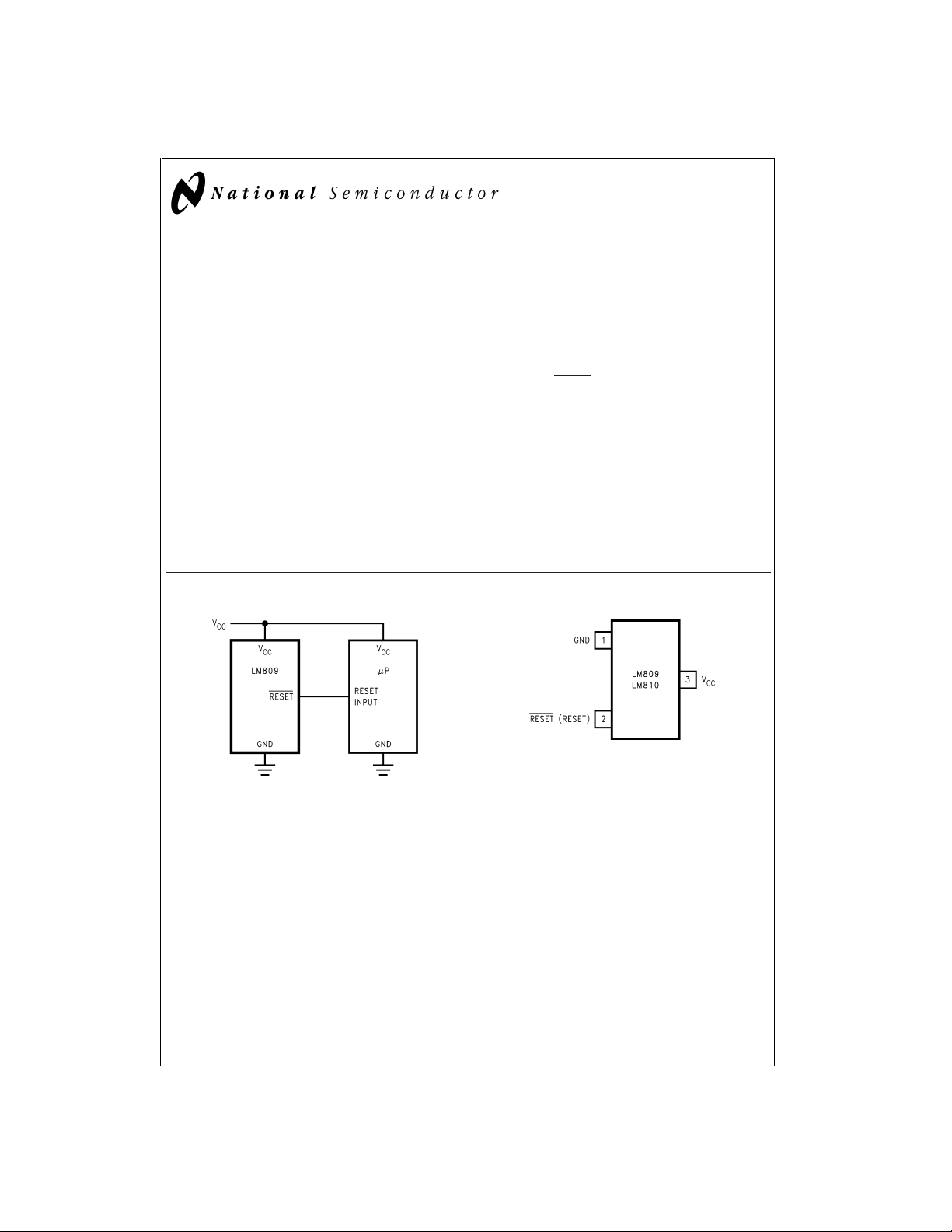
Typical Application Circuit Connection Diagram
( ) are for LM810
DS101057-1
≥1V
CC
DS101057-2
© 1999 National Semiconductor Corporation DS101057 www.national.com
Page 2
Ordering Information
Reset Threshold
(V)
LM809 Supplied as
1000 units, tape & reel
LM809 Supplied as
3000 units, tape & reel
Package
Top Mark
Package Type NSC Package
4.63 LM809M3-4.63 LM809M3X-4.63 S8B
4.38 LM809M3-4.38 LM809M3X-4.38 S7B
4.00 LM809M3-4.00 LM809M3X-4.00 S6B
3.08 LM809M3-3.08 LM809M3X-3.08 S5B
SOT23-3 M03B
2.93 LM809M3-2.93 LM809M3X-2.93 S4B
2.63 LM809M3-2.63 LM809M3X-2.63 S3B
Reset Threshold
(V)
LM810 Supplied as
1000 units, tape & reel
LM810 Supplied as
3000 units, tape & reel
Package
Top Mark
Package Type NSC Package
4.63 LM810M3-4.63 LM810M3X-4.63 SEB
4.38 LM810M3-4.38 LM810M3X-4.38 SDB
4.00 LM810M3-4.00 LM810M3X-4.00 SCB
3.08 LM810M3-3.08 LM810M3X-3.08 SBB
SOT23-3 M03B
2.93 LM810M3-2.93 LM810M3X-2.93 SAB
2.63 LM810M3-2.63 LM810M3X-2.63 S9B
Custom voltages and improved accuracies are available, subject to minimum orders. Contact your local National Semiconductor Sales Office for information.
Pin Description
PIN NAME FUNCTION
1 GND Ground reference
RESET (LM809)
2
RESET (LM810)
3V
CC
Active-low output. RESET remains low while VCCis below the reset threshold, and
for 240ms after VCCrises above the reset threshold.
Active-high output. RESET remains high while V
for 240ms after V
rises above the reset threshold.
CC
is below the reset threshold, and
CC
Supply Voltage (+5V, +3.3V, or +3.0V)
www.national.com 2
Page 3

Absolute Maximum Ratings (Note 1)
If Military/Aerospace specified devices are required,
please contact the National Semiconductor Sales Office/
Distributors for availability and specifications.
V
CC
RESET, RESET
Input Current, V
Pin 20mA
CC
Output Current, RESET, RESET Pin
Rate of Rise, V
CC
−0.3V to 6.0V
−0.3V to (VCC+ 0.3V)
20mA
100V/µs
ESD Rating (Note 2) 2kV
Continuous Power Dissipation (T
A
=
+70˚C)
SOT-23 (Note 3) 320mW
Ambient Temperature Range −40˚C to +105˚C
Maximum Junction Temperature 125˚C
Storage Temperature Range −65˚C to +160˚C
Lead Temperature (soldering,
10sec) +300˚C
Electrical Characteristics
=
V
full range, T
CC
4.63/4.38/4.00 versions, V
Symbol Parameter Conditions Min Typ Max Units
V
Supply Current
I
CC
Reset Threshold (Note 5)
V
TH
Reset Threshold
Temperature Coefficient
V
5)
Reset Active Timeout
Period
RESET Output Voltage Low
V
OL
(LM809)
=
−40˚C to +105˚C, unless otherwise noted. Typical values are at T
A
CC
Range
CC
to Reset Delay (Note
CC
=
3.3V for 3.08/2.93 versions, and V
=
T
0˚C to +70˚C 1.0 5.5
A
=
−40˚C to +105˚C 1.2 5.5
T
A
=
T
−40˚C to
A
+85˚C
=
T
+85˚C to
A
+105˚C
LM8_ _ -4.63
LM8_ _ -4.38
LM8_ _ -4.00
LM8_ _ -3.08
LM8_ _ -2.93
LM8_ _ -2.63
=
V
CC
T
A
T
A
V
CC
LM809-2.63/2.93/3.08
CC
LM809-4.63/4.38/4.00
V
CC
to (VTH− 100mV) 20 µs
V
TH
=
−40˚C to +85˚C 140 240 560
=
+85˚C to +105˚C 100 840
=
min, I
V
TH
=
min, I
V
TH
>
1.0V, I
SINK
=
+25˚C, V
=
3V for 2.63 version. (Note 4)
CC
<
5.5V, LM8_ _
V
CC
-4.63/4.38/4.00
<
3.6V, LM8_ _
V
CC
-3.08/2.93/2.63
<
5.5V, LM8_ _
V
CC
-4.63/4.38/4.00
<
V
3.6V, LM8_ _
CC
-3.08/2.93/2.63
=
T
+25˚C 4.56 4.63 4.70
A
=
T
−40˚C to +85˚C 4.50 4.75
A
=
T
+85˚C to +105˚C 4.40 4.86
A
=
+25˚C 4.31 4.38 4.45
T
A
=
T
−40˚C to +85˚C 4.25 4.50
A
=
T
+85˚C to +105˚C 4.16 4.56
A
=
+25˚C 3.93 4.00 4.06
T
A
=
T
−40˚C to +85˚C 3.89 4.10
A
=
T
+85˚C to +105˚C 3.80 4.20
A
=
+25˚C 3.04 3.08 3.11
T
A
=
T
−40˚C to +85˚C 3.00 3.15
A
=
T
+85˚C to +105˚C 2.92 3.23
A
=
+25˚C 2.89 2.93 2.96
T
A
=
T
−40˚C to +85˚C 2.85 3.00
A
=
T
+85˚C to +105˚C 2.78 3.08
A
=
+25˚C 2.59 2.63 2.66
T
A
=
T
−40˚C to +85˚C 2.55 2.70
A
=
T
+85˚C to +105˚C 2.50 2.76
A
A
=
5V for
CC
18 60
15 50
30 ppm/˚C
=
1.2mA,
SINK
=
3.2mA,
SINK
=
50µA 0.3
100
100
0.3
0.4
V
µA
V
ms
VV
www.national.com3
Page 4

Electrical Characteristics (Continued)
=
V
full range, T
CC
4.63/4.38/4.00 versions, V
Symbol Parameter Conditions Min Typ Max Units
V
V
V
Note 1: Absolute Maximum Ratings are limits beyond which damage to the device may occur. Operating Ratings are conditions under which the device operates
correctly. Operating ratings do not imply guaranteed performance limits. For guaranteed performance limits and associated test conditions, see the Electrical Characteristics.
Note 2: The human body model is a 100pF capacitor discharged through a 1.5kΩ resistor into each pin.
Note 3: Production testing done at T
Note 4: At elevated temperatures, devices must be derated based on package thermalresistance.The device in the SOT23-3 package must be derated at 4mW/˚C
at ambient temperatures above 70˚C. The device has internal thermal protection.
Note 5: RESET Output for LM809, RESET output for LM810.
RESET Output Voltage
OH
High (LM809)
RESET Output Voltage Low
OL
(LM810)
RESET Output Voltage
OH
High (LM810)
=
−40˚C to +105˚C, unless otherwise noted. Typical values are at T
A
=
3.3V for 3.08/2.93 versions, and V
CC
>
V
VTHmax, I
CC
LM809-2.63/2.93/3.08
>
VTHmax, I
V
CC
LM809-4.63/4.38/4.00
=
V
V
CC
LM810-2.63/2.93/3.08
=
V
V
CC
LM810-4.63/4.38/4.00
<
1.8V
V
=
+25˚C, over temperature limits guaranteed by design only.
A
TH
TH
CC
max, I
max, I
<
VTHmin, I
SOURCE
SOURCE
SINK
SINK
=
3V for 2.63 version. (Note 4)
CC
=
500µA,
=
800µA,
=
1.2mA,
=
3.2mA,
=
SOURCE
150µA
A
=
0.8V
V
0.8V
+25˚C, V
CC
−1.5
CC
CC
=
5V for
CC
V
0.3
0.4
V
V
Typical Performance Characteristics
Supply Current vs Temperature
(No Load, LM8_ _-2.63/2.93/3.08)
DS101057-3
Power-Down Reset Delay vs
Temperature (LM8_ _-4.63/4.38)
DS101057-6
Supply Current vs Temperature
(No Load, LM8_ _-4.63/4.38)
DS101057-4
Power-Up Reset Timeout vs
Temperature
DS101057-7
Power-Down Reset Delay vs Temp
(LM8_ _-2.63/2.93/3.08)
DS101057-5
Normalized Reset Threshold vs
Temperature
DS101057-8
www.national.com 4
Page 5

Applications Information
Benefits of Precision Reset Thresholds
A microprocessor supply supervisor must provide a reset
output within a predictable range of the supply voltage. A
common threshold range is between 5%and 10%below the
nominal supply voltage. The 4.63V and 3.08V options of the
LM809/810 use highly accurate circuitry to ensure that the
reset threshold occurs only within this range (for 5V and 3.3V
supplies). The other voltage options have the same tight tolerance to ensure a reset signal for other narrow monitor
ranges. See
thresholds apply to 3V, 3.3V, and 5V nominal supply voltages.
Table1
for examples of how the standard reset
Negative-Going V
Transients
CC
The LM809/810 are relatively immune to short
negative-going transients or glitches on V
the maximum pulse width a negative-going V
can have without causing a reset pulse. In general, as the
CC
.
Figure 2
CC
shows
transient
magnitude of the transient increases, going further below the
threshold, the maximum allowable pulse width decreases.
Typically, for the 4.63V and 4.38V version of the LM809/810,
aV
transient that goes 100mV below the reset threshold
CC
and lasts 20µs or less will not cause a reset pulse. A 0.1 µF
bypass capacitor mounted as close as possible to the V
pin will provide additional transient rejection.
CC
TABLE 1. Reset Thresholds Related to Common
Supply Voltages
Reset
Threshold
±
3
4.63
±
4.38
3
±
4.00
3
±
3.08
3
±
2.93
3
±
2.63
3
Ensuring a Valid Reset Output Down to V
When V
CC
longer sinks current. A high-impedance CMOS logic input
3.0V 3.3V 5.0V
%
%
%
%
%
%
85-90%77-81
90-95
86-90
%
%
%
90-95
85-90
78-82
=
CC
%
%
%
0V
falls below 1V, the LM809 RESET output no
connected to RESET can therefore drift to undetermined
voltages. To prevent this situation, a 100kΩ resistor should
be connected from the RESET output to ground, as shown in
Figure 1
.
A100kΩ pull-up resistor to V
LM810, if RESET is required to remain valid for V
is also recommended for the
CC
CC
<
1V.
DS101057-9
FIGURE 2. Maximum Transient Duration without
Causing a Reset Pulse vs. Reset Comparator
Overdrive
Interfacing to µPs with Bidirectional Reset Pins
Microprocessors with bidirectional reset pins, such as the
Motorola 68HC11 series, can be connected to the LM809
RESET output. To ensure a correct output on the LM809
even when the microprocessor reset pin is in the opposite
state, connect a 4.7kΩ resistor between the LM809 RESET
output and the µP reset pin, as shown in
Figure 3
. Buffer the
LM809 RESET output to other system components.
FIGURE 1. RESET Valid to V
DS101057-10
=
Ground Circuit
CC
DS101057-11
FIGURE 3. Interfacing to Microprocessors with
Bidirectional Reset I/O
www.national.com5
Page 6

Physical Dimensions inches (millimeters) unless otherwise noted
For Ordering, refer to Ordering Information table
3-Lead SOT23-3
NS Package Number M03B
LM809/LM810 3-Pin Microprocessor Reset Circuits
LIFE SUPPORT POLICY
NATIONAL’S PRODUCTS ARE NOT AUTHORIZED FOR USE AS CRITICAL COMPONENTS IN LIFE SUPPORT
DEVICES OR SYSTEMS WITHOUT THE EXPRESS WRITTEN APPROVAL OF THE PRESIDENT AND GENERAL
COUNSEL OF NATIONAL SEMICONDUCTOR CORPORATION. As used herein:
1. Life support devices or systems are devices or
systems which, (a) are intended for surgical implant
into the body, or (b) support or sustain life, and
whose failure to perform when properly used in
accordance with instructions for use provided in the
labeling, can be reasonably expected to result in a
significant injury to the user.
National Semiconductor
Corporation
Americas
Tel: 1-800-272-9959
Fax: 1-800-737-7018
Email: support@nsc.com
www.national.com
National Semiconductor
Europe
Fax: +49 (0) 1 80-530 85 86
Email: europe.support@nsc.com
Deutsch Tel: +49 (0) 1 80-530 85 85
English Tel: +49 (0) 1 80-532 78 32
Français Tel: +49 (0) 1 80-532 93 58
Italiano Tel: +49 (0) 1 80-534 16 80
2. A critical component is any component of a life
support device or system whose failure to perform
can be reasonably expected to cause the failure of
the life support device or system, or to affect its
safety or effectiveness.
National Semiconductor
Asia Pacific Customer
Response Group
Tel: 65-2544466
Fax: 65-2504466
Email: sea.support@nsc.com
National Semiconductor
Japan Ltd.
Tel: 81-3-5639-7560
Fax: 81-3-5639-7507
National does not assume any responsibility for use of any circuitry described, no circuit patent licenses are implied and National reserves the right at any time without notice to change said circuitry and specifications.
 Loading...