

Page 1
PREPARED
BY: DATE
SPEC No. LC99404
FILE No.
SHARP
I
_)__oBI:D_ SHARPCORPORATION
LIQUID CRYSTAL DISPLAY GROUP
SPECIFICATION
DEVICE SPECIFICATION for
Passive Matrix Monochrome LCD Module
(640X240 dots)
ISSUE APR. 28.1999
PAGE 25 Pages
REPREZNTATIVE DMSION
ENGINEERING DEPARTMENT I
DUTY LCD
DUTY LIQUID CRYSTAL
DISPLAY GROUP
DEVELOPMENT CENTER
I
q
CUSTOMER’S APPROVAL
DATE
BY
Model No.
LM7MS623
PRESENTED
r
--
DEPARTMENT
ENGINEERING DEPARTMENT I
DUTY LCD DEVELOPMENT CENTER
DUTY LIQUID CRYSTAL DISPLAY GROUP
SHARP CORPORATION
GENERAL MANAGER
Page 2
SHARP
JWCORDS OF REVISION
DATE REF.PAGE REVISED SUMMARY CHECK
PARAGRAPH
DRAWING No. NO. APPROVAL
DOC.FIRST ISSUE
APR.28 1999
Page 3
SHARP
0
Precautions
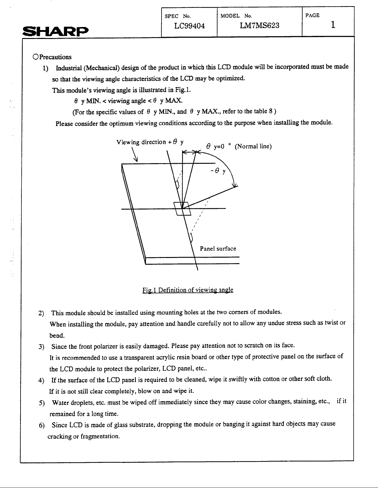
1) Industrial (Mechanical) design of the product in which this LCD module will be incorporated must be made
so that the viewing angle characteristics of the LCD may be optimized.
This module’s viewing angle is illustrated in Fig.1.
Please consider the optimum viewing conditions according to the purpose when installing the module.
SPEC No.
LC99404
8 yMIN.<viewingangle<0 yMAX.
(For the specific values of 0 y MIN., and 8 y MAX., refer to the table 8 )
MODEL No.
LM7MS623
PAGE
1
Viewing direction + 6 y
Fig.1 Definition of viewine angle
This module should be installed using mounting holes at the two corners of modules.
2)
When installing the module, pay attention and handle carefully not to allow any undue stress such as twist or
y=O
’ (Normal line)
Panel surface
bend.
Since the front polarizer is easily damaged. Please pay attention not to scratch on its face.
3)
It is recommended to use a transparent acrylic resin board or other type of protective panel on the surface of
the LCD module to protect the polarizer, LCD panel, etc..
If the surface of the LCD panel is required to be cleaned, wipe it swiftly with cotton or other soft cloth.
4)
If it is not still clear completely, blow on and wipe it.
Water droplets, etc. must be wiped off immediately since they may cause color changes, staining, etc.,
5)
remained for a long time.
Since LCD is made of glass substrate, dropping the module or banging it against hard objects may cause
6)
cracking or fragmentation.
if it
Page 4
SPEC No. MODEL No. PAGE
LC99404 LM7MS623
SHARP
7) Since CMOS LSIs are equipped in this module, following countermeasures must be taken to avoid
electrostatics charge.
l-Operator
Electrostatic shielding clothes shall be had because it is feared that the static electricity is electrified to
human body in case that operator have a insulating garment.
2.Equipmeot
There is a possibility that the static electricity is charged to equipment which have a function of peeling or
mechanism of friction(EX: Conveyer, soldering iron, working table), so the countermeasure(electrostatic
earth:1 X lo8 Q) should be made.
3.Floor
Floor is a important part to leak static electricity which is generated from human body or equipment.
There is a possibility that the static electricity is charged to them without leakage in case of insulating
floor,so the countermeasure(electrostatic earth: 1 X 10’ Q ) should be made.
4.Humidity
2
Humidity of working room may lower electrostatics generating material’s resistance and have something to
prevent electrifying. So, humidity should be kept over 50% because humidity less than 50 % may increase
material’s electrostatic earth resistance and it become easy to electrify.
S.Transportation/storage
The measure should be made for storage materials because there is a possibility that the static electriicity,
which electrify to human body or storage materials like container by friction or peeling, cause the dielectric
charge.
6.0thers
The laminator is attached on the surface of LCD module to prevent from scratches, fouling and dust.
It should be peeled off unhurriedly with using static eliminator.
And also, static eliminator should be installed to prevent LCD module from electrifying at assembling line.
8) Don’t use any materials which emit gas from epoxy resin(amines’
agent(dealcohol or deoxym) to prevent change polorizer color owing to gas.
9) Avoid to expose the module to the direct sun-light, strong ultraviolet light, etc. for a long time.
10) If stored at temperatures under specified storage temperature, the LC may freeze and be deteriorated.
If storage temperature exceed the specified rating, the molecular orientation of the LC may change to that of
a liquid, and they may not revert to their original state. Therefore, the module should be always stored at norma
hardener) and silicon adhesive
room temperature.
11) Disassembling the LCD module can cause permanent damage and should be strictly avoided.
Page 5
SPEC No.
LC99404 LM7MS623
MODEL No. PAGE
SHARP
12) Do not use touch TCP/LCD connection area to prevent interconnection breakdown.
13) Do not apply organic solvent to TWLCD connection area where organic materials are used.
14) This specification describes display quality in case of no gray scale. Since display quality can be affected by
gray scaIe methods, display quality shall be carefully evaluated for the usability of LCD module in case gray
scale is displayed on the LCD module.
15) The module should be driven according to the specified ratings to avoid permanent damage.
DC voltage drive leads to rapid deterioration of LC, so ensure that the drive is alternating waveform by
continuous application of the signal M. Esneciallv the Dower ON/OFF seauence shown on Pave 22 should be
kent to avoid latch-un of drive LSI and application of DC voltape to LCD Dane1
3
Page 6
SHARP
SPEC No.
LC99404
MODEL No.
LM7MS623
PAGE
4
OContents
LApplication
2.Construction and Outline
3.Mechanical Specifications
4.Absolute Maximum Ratings
4-1.Electrica.l absolute maximum ratings
4-2.Enviroment Conditions
S.Electrical Specifications
5-l.Electrical characteristics
5-2.Interface signals -
6.Module Driving Method
6-l.Circuit configuration
6-2.Display face configuration
6-3Jnput data and control signal
7.0ptical Characteristics
8.Supply voltage sequence condition
9.Lot number
Page
5
6
7
8
9
14
16
22
23
lO.Applicable Inspection Standard
ll.LCD Module out line dimension.
24
Page 7
SPEC No.
MODEL No.
PAGE
LC99404
SHARP
LM’7MS623
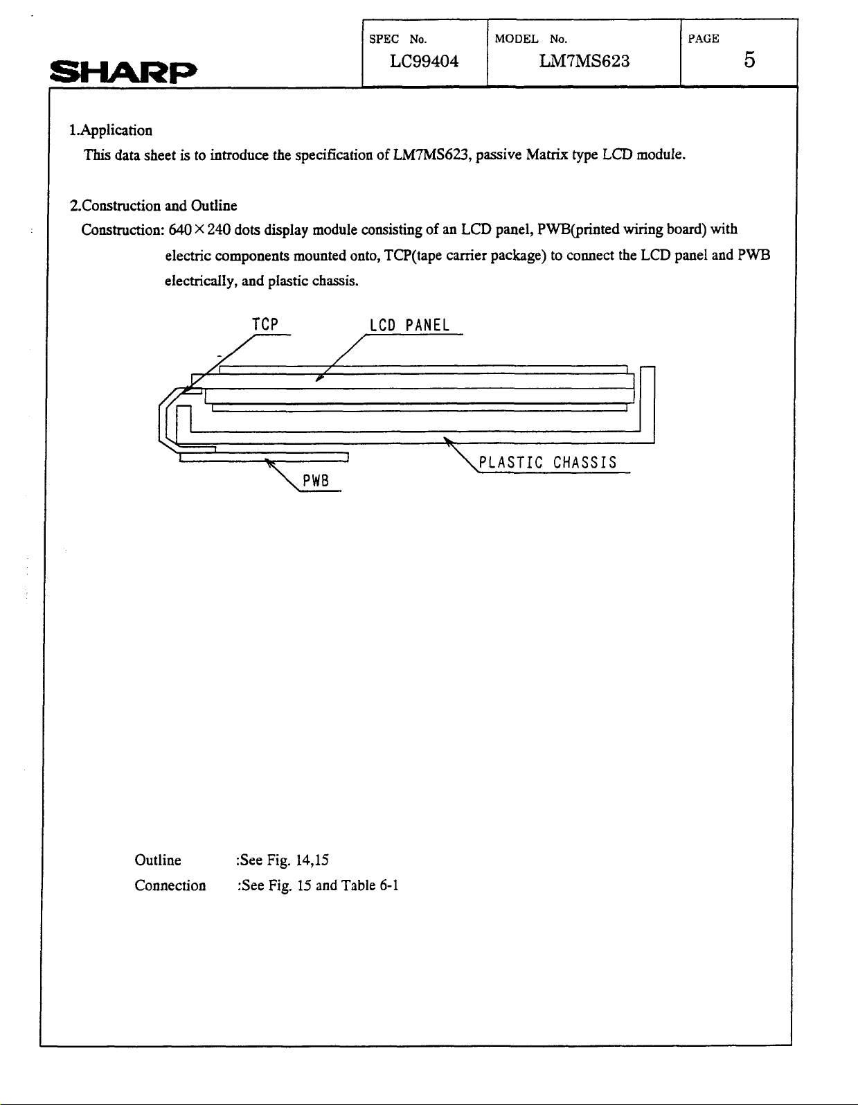
1Application
This data sheet is to introduce the specification of LM7MS623, passive Matrix type LCD module.
Z.Construction and Outline
Construction: 640 X 240 dots display module consisting of an LCD panel, PWEQrinted wiring board) with
electric components mounted onto, TCP(tape carrier package) to connect the LCD panel and PWB
electrically, and plastic chassis.
I/
TCP
Y
/
LCD PANEL
1
.
PLASTIC CHASSIS
v-l
I
PWB
5
Outline
Connection
:See Fig. 14,lS
:See Fig. 15 and Table 6-1
Page 8
SHARP
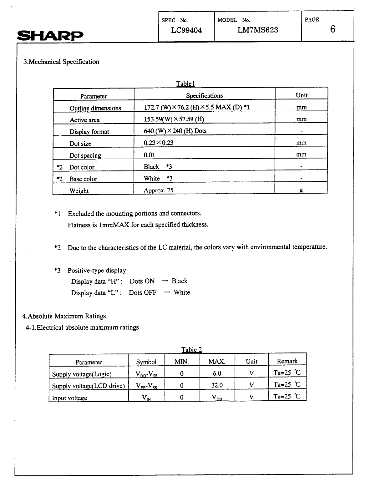
3.Mechanical Specification
SPEC No. MODEL No.
LC99404 LM7MS623
Table1
PAGE
6
* 1 Excluded the mounting portions and connectors.
Flatness is 1mmMAX for each specified thickness.
*2 Due to the characteristics of the LC material, the colors vary with environmental temperature.
‘3 Positive-type display
Display data “I-I” :
Display data “L” : Dots OFF - White
4.Absolute Maximum Ratings
4-l.Electrical absolute maximum ratings
Dots ON - Black
Page 9
SHARP
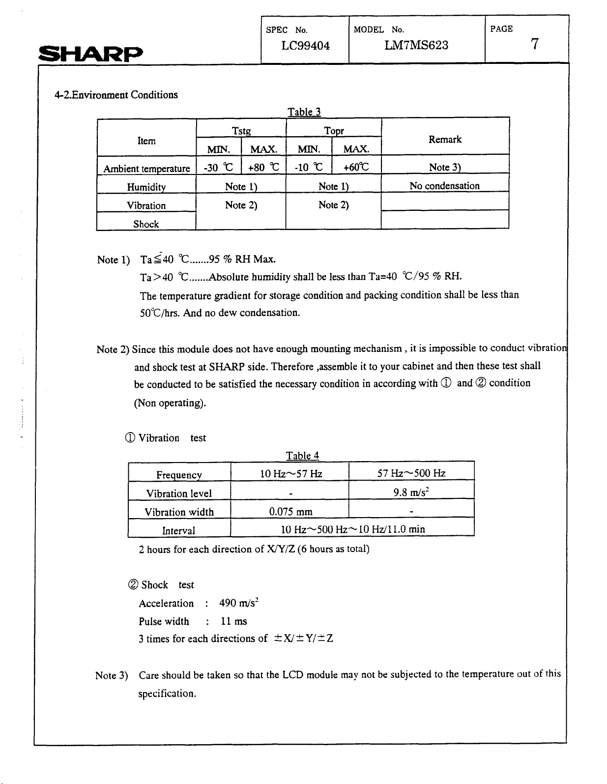
4-2.Environment Conditions
SPEC No.
LC99404
Table 3
MODEL No.
LM7MS623
PAGE
7
Item
Ambient temperature -30 “c +80 “c
Humidity
Vibration Note 2)
Shock
Note 1) Tag40 “C.. .... .95 % RH Max.
Ta>40 “C .....
The temperature gradient for storage condition and packing condition shall be less than
5O”Uhrs. And no dew condensation.
Note 2) Since this module does not have enough mounting mechanism,
and shock test at SHARP side. Therefore ,assemble it to your cabinet and then these test shall
be conducted to be satisfied the necessary condition in according with 0 and @ condition
(Non operating).
Tstg Topr
MIN. MAX. MIN. MAX.
-10 “c +6O”c
Note 1) Note 1)
Note 2)
..AbsoIut e humidity shall be less than Ta=40 “C/95 % RH.
Remark
Note 3)
No condensation
it is impossible to conduct vibratio.
0 Vibration test
Table 4
Frequency
Vibration level
Vibration width
Interval
2 hours for each direction of X/Y/Z (6 hours as total)
@ Shock test
Acceleration : 490 m/s’
Pulse width : llms
3 times for each directions of t X/ t Y/k Z
Note 3) Care should be taken so that the LCD module may not be subjected to the temperature out of this
specification.
10 Hz-57 Hz 57 Hz-500 Hz
-
0.075 mm
10 Hz-500 Hz- 10 Hz/l 1.0 min
9.8 m/s’
Page 10

SPEC No. MODEL No.
PAGE
,SHARP
5EIectricaI Specifications
5-l.Electrical characteristics
Supply voltage (LCD)
Input leakage current
Supply current (Logic)
LC99404 LM7MS623
Table 5-l
8
Note 1) The voltage [VEE-VSS] for obtaining maximum contrast is different in individual modules.
And it change because of temperature.
Therefor it is needed adjusting the voltage [VEE-VSS] for obtain to proper contrast.
Note 2) Under the following condition.;
VDD-VSS=3.3V, VEE-VSS=20.9V, Frame frequency=70Hz, Ta=25”C
Display pattem=Full dots ON
Note 3) Under the following condition.;
VDD-VSS=3.3V, VEE-VSS=20.9V, Frame frequency=70Hz, Ta=25”C
Display
pattern
¤0a0~nBoucl~clm0m0BclBn
clmclaclmcl~a~omCBo~clmcla
~0~0~0~0~0~0~0~0~0~0
Page 11

SPEC No. MODEL No.
PAGE
52.Interface signals
LC99404 LM7MS623
Display data signal
9
Note 1) these signals are not concerned with driving the LCD module.
Table 6-2 CN2
Pin No. SymboI
1 C Extra signals
2 D
3 E
4
Pin No Svmbol Descriotion Note
1 A Extra signals
2
Used connector CNl : SM02B-SSR-H [JST]
Correspondable connector CNl : 02SSR-32H [JST]
Except above connector shall be out of guaranty.
F
Table 6-3 CNl
B
CN2 : 04 6227 004 100 800 [KYOCERA ELCO]
CN3 : 0.3mm pitch ,FPC
CN2 :l.Omm pitch ,FPC/FFC
CN3 :FH12-22S-0.5SH [HIROSE]
Description
(for Touch panel signal)
(for Lo& level oniv)
Note
Page 12

--------------------
1240.1-__---_-_____________________
___________
I240.Ea0
SHARP
ROW
\
ldat -
2dat -
3dat -
COLUMN
ldat 2dat
I I
3dat
pp+
SPEC No.
LC99404
I
MODEL No.
Lii7MS623
PAGE
10
64Cldat
t
_ ---- $-ei
240dat -
MO c2doc -
3dot-
240doc-
II !I
>
Note) 1,2 means 1 st row 2nd column dot.
Fig. 1
Dot
chart of display area
Page 13

SHARP
SPEC No. MODEL No.
LC99404
LM7MS623
PAGE
11
r-27
’ CPI r
DO-3 2 1, (1 -ma :(
S
<
me-
e-e
I
---
CP 1 x 240 pu I se5
240. (l-640) )(I, (l-640) >(
3
Fie. 2 Data inout timimz chart
:::-3c
Page 14

SPEC No. MODEL No.
PAGE
SHARP
LC99404 LM7MS623
12
M
,
CPI
s
I
-
f
i
44
9 rst
ine's
iata
transfer transfer
-4-J
data
sec=nd
1 ine’s
TF3klZ.j
C?t x 260 zulese
4 14.3 ms I
,
I
M
b 3
Interface tusz chart
Page 15

SHARF)
SPEC No.
LC99404
MODEL No.
LM7MS623
PAGE
13
Note 1)
Note 2)
h-f=50
trf =tc-J
S signal data hold time
S T clock allowance time from CPl 1 tcp1s 100 -
M delay time
Owing to the characteristics of LCD module, ~‘shadowing” will become more eminent as frame frequency
goes up, flicker will become more eminent as frame frequency goes down. So it is recommended that the
module should be driven according to the specified limit.
incase tcr= (TCPZ- tCWH - tCWL) / 28 50
in case b= (TCP2 - tCWH - tCWL) / 2 < 50
tSH loo -
th4 -
50 ns
ns
ns
Page 16

SHARP
6. Module Driving Method
6-l. Circuit configuration
Fig. 11 shows the block diagram of the module’s circuitry.
6-2. Display face configuration
The display consists of 640 X 240 dots as shown in Fig. 2.
The interface is single panel with single drive to be driven at l/240 duty ratio.
6-3. ‘Lnput data and cqntrol signal
The LCD driver is 160 bits LSI, consisting of shift registers, latch circuits and LCD driver circuits.
Display data which are externally divided into data for each row (640 dots) will be sequentially
transferred in the form of 4- bit parallel data through shift registers by Clock Signal CP2 from the left
top of the display face.
SPEC No. MODEL No.
LC99404 LM7MS623
PAGE
14
When input of one row (640 dots) is completed, the data will be latched in the form of parallel
data for 640 lines of signal electrodes by latch signal (CPl) then, the corresponding drive signals
will be transmitted to the 640 lines of column electrodes of the LCD panel by the LCD drive circuits.
At this time, scan start-up signal (S) has been transferred from the scan signal driver to the
electrodes, and the contents of the data signals are displayed on the 1st rows of the display face according to
the combinations of voltages applied to the scan and signal electrodes of the LCD.
While the 1st rows of data are being displayed, the 2nd row of data are entered. When 640 dots of
data have been transferred, they latched on the falling edge of CPl clock, the display face proceeds to the
2nd rows of display.
Such data input will be repeated up to the 240th row of each display segment, from upper row to lower
rows,
to complete one frame of display by time sharing method.
Then data input proceeds to the next display frame.
Scan start -up signal S generates scan signal to drive horizontal electrodes.
1st
row of scan
Since DC voltage, if applied to LCD panel, causes chemical reaction which will deteriorate LCD panel.
drive wave-form shall be inverted at every display frame to prevent the generation of such DC voltage.
Control signal M plays such a role.
Page 17

SPEC No. MODEL No.
PAGE
SHARP
Because of the characteristics of the CMOS driver LSI, the power consumption of the display module goes up
as the operating frequency CP2. Thanks to the 4 lines of shift registers to reduce the data transfer speed CP2
Thanks to the LSI, the power consumption of the display module will be minimized.
In this circuit configuration, 4-bit display data shalI be therefore input to data input pins of DO -3.
Furthermore, the display module has bus line system for data input to minimize the power consumption with
data input termin& of each driver LSI being activated only when relevant data input is fed.
Data input for column electrodes and chip select of driver LSI are made as follows:
The driver LSI at the left end of the display face is first selected, and the adjacent driver LSI of the right
next side is selected when data of 160 dot (4OCP2) is fed. This process is sequentially continued until data is
LC99404 Livl7MS623
15
fed to the driver LSI at the right end of the display face.
Thus data input will be made through 4-bit bus line sequentially from the left end of the display face.
Since this display module contains no refresh RAM, it requires the above data and timing pulse inputs even for
static display.
The timing chart of input signals are shown in fig. 3 and Table 7.
Page 18

SHARP
7.Optical Characteristics
SPEC No. MODEL No.
LC99404 LM7MS623
PAGE
16
Following spec are based upon
direction( f3 x = 0 y=O’ )willbeMAX..
Parameter
Viewing angle range
Symbol
8X
the
electrical measuring conditions, on which the contrast of perpendicular
Table 8
Condition
co12
1 ; 2 Iii Notel)
I9 y<O" - -
8
x=8
Contrast ratio
Note 1) The viewing angle range is defined as shown Fig.4.
co
z r
td
8 x=e
I9 x=e v=o o
y=o o 4 6 - - Note2) Fig.5
y=o o
Ta=25”C, Frame frequency=70Hz
1/240DUTY, Vu,-V, = 3.3 V, V,,-V, = Vmax
MIN.
Measureing spot size : Q 1Omm
TYP. MAX. Unit
-25 dgr.
8 10 - - Fig.8
190 240 ms
220 270 ms
Remark
Note3)
-eY
vote 2) Contrast ratio is defined as follows:
co Luminance@rightness) all pixes “White” at Vmax
= Luminance@rightness) all pixes “dark ” at Vmax
Vmax is defined in Fig.6.
+eY
tex
\
-eY
Definition of Viewing Anlzle Fi .4 e
Vote 3) The response characteristics of photodetector output are measured as shown in Fig.9, assuming that input
signals are applied so as to select and deselect the dot to be measured, in the optical characteristics test
method shown in Fig.10.
Page 19

SHARP
SPEC No.
LC99404
MODEL No.
N7MS623
PAGE
17
Comax.
-- normal
Measuring Spot Size : # 10 mm
8 x: Angle from “normal” to viewing surface rotated about the horizontal axis.
e
y: Angle from “normal” to viewing surface rotated about the vertical axis.
Fig.5 Optical Characteristics Test Method I
Measuring
Field: 2 ’
Vmax .
Fig.6 Detinition of Vmax
> VEE (V)
Page 20

SHARP
SPEC No.
LC99404
Sumey Place : @-@
Meiwxement spat size : 10 mm 4
i -y=L
MODEL No.
LM7MS623
PAGE
18
x=1
Light source
X=160 X=320
Fig.7 Measuring points(l-5)
Nod
line
t’
I
,
3,: Heasurernent spot size:0.2 ma4
-\
\
\
J
\
\
I
,
I
x=480
\
L?i
,’
I
I
I
I
,
,
I
I
’ .
I
I
60-O= 30
X=640
Photo-detector
(Included a viewing
sensitivity modulator
l
‘f--LCD panel
Rer’lec
Fig. 8 Optical Characteristics Test Method [I
tar
Page 21

SHARP
(Response Measurement)
Ta=25 “C
In dark room
SPEC No.
LC99404 LM7MS623
MODEL No.
PAGE
19
LCD Module
cl
_’
Computer
I
.’
normal
w
TOPCON BM7 + quartz fiber
(Measuring spot size : @ 10 mm, Measuring Field : 2
Fip. 9 Optical Characteristics Test Method I
8 x=8 y=o”
\
I
1
Page 22

SPEC No. MODEL No.
PAGE
SHARP
[
Drive
Non-select
- uare?arrJ
raveform I 1
n
-
1
LC99404 LM7MS623
1
Select
w wa7efarm -
20
Non-select
[ Responce waveform 1
A
K r:
K d: Decay time
Rise time
L
Fip 10 Difinition of ResDonse Time
Page 23

SHARP
SPEC No. lMODEL No.
LC99404
LM7MS623
PAGE
21
Bias Voltage
Generator
VDD -
CPl
CP2
DISP
r
(1,640)
(2,640)
640 X 240 DOTS LCD PANEL
(240,640)
SEG Drive
I
Fie. I1 Circuit block diagram
Page 24

SHARP
9.Supply voltage sequence condition
The power ON/OFF sequence shown on Fig.12 shall be followed to avoid latch-up of drive LSI and application
0fDC voltage to LCD panel.
81, CP2
DATA, H
SPEC No.
LC99404
iMODEL No.
LM7MS623
PAGE
22
DISP
SYMBOL
a
b
C
d
e I -
f
e
L
m
,
/
Fig.12 Power ON/OFF seauence
Table 9 Seauence timine rating
POWER ON
With DISP Without DISP SYMBOL 1 WithDISP 1 without DISP
control
OIIlS.blIN. OmSMIN.
OUlSMIN. 2oLnsmN.
2oIIlsmN.
OmSlMlN.
OUlSMIN. (Note 2)
s
control
2omsMAx.
w
e
OmSMIN.
2omsMIN.
j
I
L
I m I Oms~MlN. I (Notc2) I
n I -
POWER OFF
control
1 2omsMIN. )
I -
control
-
OIIISMIN.
I 0mslaN. 1
1
Note 1) Power ON/OFF cycle time. All signals and power line shall be in accordance with above
sequence in case of power ON/Off.
-
Note 3-J VEE to be set at “VSS level”
Page 25

SPEC No.
LC99404
iMODEL No.
LM7MS623
PAGE
lO.Lot number
Lot number is shown at the position mentioned in Fig .13 in accordance with the following numbering rule.
(ExampIe)
Factory Identification Code. (Alphabet)
Serial number (Missing number exist.)
Production month (A=JAN.,B=FEB.;**L=DEC.)
Production year.
23
Fie.13.
ll.Applicable inspection standard
The LCD panel shall meet the following inspection standard :
S-U-012-01
Page 26

t
76 2to :
?I
c
6
B
/
.-. -
i-
D
c
3
m
7
:
57i
0)
N
ln
J
P
w
A
tp
Y
13.
116. 50.3
Page 27

L -L--Au--
I I
I -i
N
%
X
11
Page 28

graphics, HVGA, 1/2 VGA, monochrome, passive, LM7MS623
 Loading...