

Datasheet LM79L15ACMX, LM79L15ACMWA, LM79L15ACM, LM79L12ACMWA, LM79L12ACMDA Datasheet (NSC)
...Page 1
LM320L/LM79LXXAC/LM13121 Series
3-Terminal Negative Regulators
General Description
The LM320L/LM79LXXAC/LM13121 dual marked series of
3-terminal negative voltage regulators features fixed output
voltages of −5V, −12V, and −15V with output current capabilities in excess of 100mA. These devices were designed
using the latest computer techniques for optimizing the packaged IC thermal/electrical performance. The LM79LXXAC
series, even when combined with a minimum output compensation capacitor of 0.1µF, exhibits an excellent transient
response, a maximum line regulation of 0.07% V
O
/V, and a
maximum load regulation of 0.01% V
O
/mA.
The LM320L/LM79LXXAC/LM13121 series also includes, as
self-protection circuitry: safe operating area circuitry for output transistor power dissipation limiting, a temperature independent short circuit current limit for peak output current
limiting, and a thermal shutdown circuit to prevent excessive
junction temperature. Although designed primarily as fixed
voltage regulators, these devices may be combined with
simple external circuitry for boosted and/or adjustable voltages and currents. The LM79LXXAC series is available in
the 3-lead TO-92 package, 8-lead SOIC package, and the
6-Bump micro SMD package. The LM320L series is available in the 3-lead TO-92 package.
For output voltage other than −5V, −12V and −15V, the
LM137L series provides an output voltage range from 1.2V
to 47V.
Features
n Preset output voltage error is less than±5% overload,
line and temperature
n Specified at an output current of 100mA
n Easily compensated with a small 0.1µF output
capacitor
n Internal short-circuit, thermal and safe operating area
protection
n Easily adjustable to higher output voltages
n Maximum line regulation less than 0.07% V
OUT
/V
n Maximum load regulation less than 0.01% V
OUT
/mA
n See AN-1112 for micro SMD considerations
Typical Applications
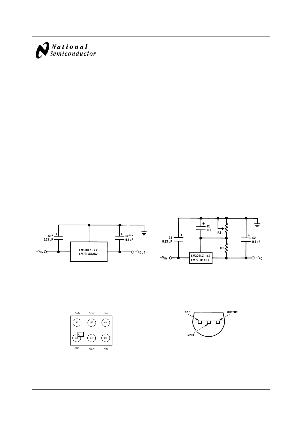
Fixed Output Regulator
00774801
*Required if the regulator is located far from the power supply filter. A 1µF
aluminum electrolytic may be substituted.
*
*
Required for stability. A 1µF aluminum electrolytic may be substituted.
Adjustable Output Regulator
00774803
−V0= −5V − (5V/R1 + IQ)•R2,
5V/R1
>
3I
Q
Connection Diagrams
6-Bump micro SMD
00774820
Bump Side Down
TO-92 Plastic Package (Z)
00774802
Bottom View
January 2003
LM320L/LM79LXXAC/LM13121 Series 3-Terminal Negative Regulators
© 2003 National Semiconductor Corporation DS007748 www.national.com
Page 2
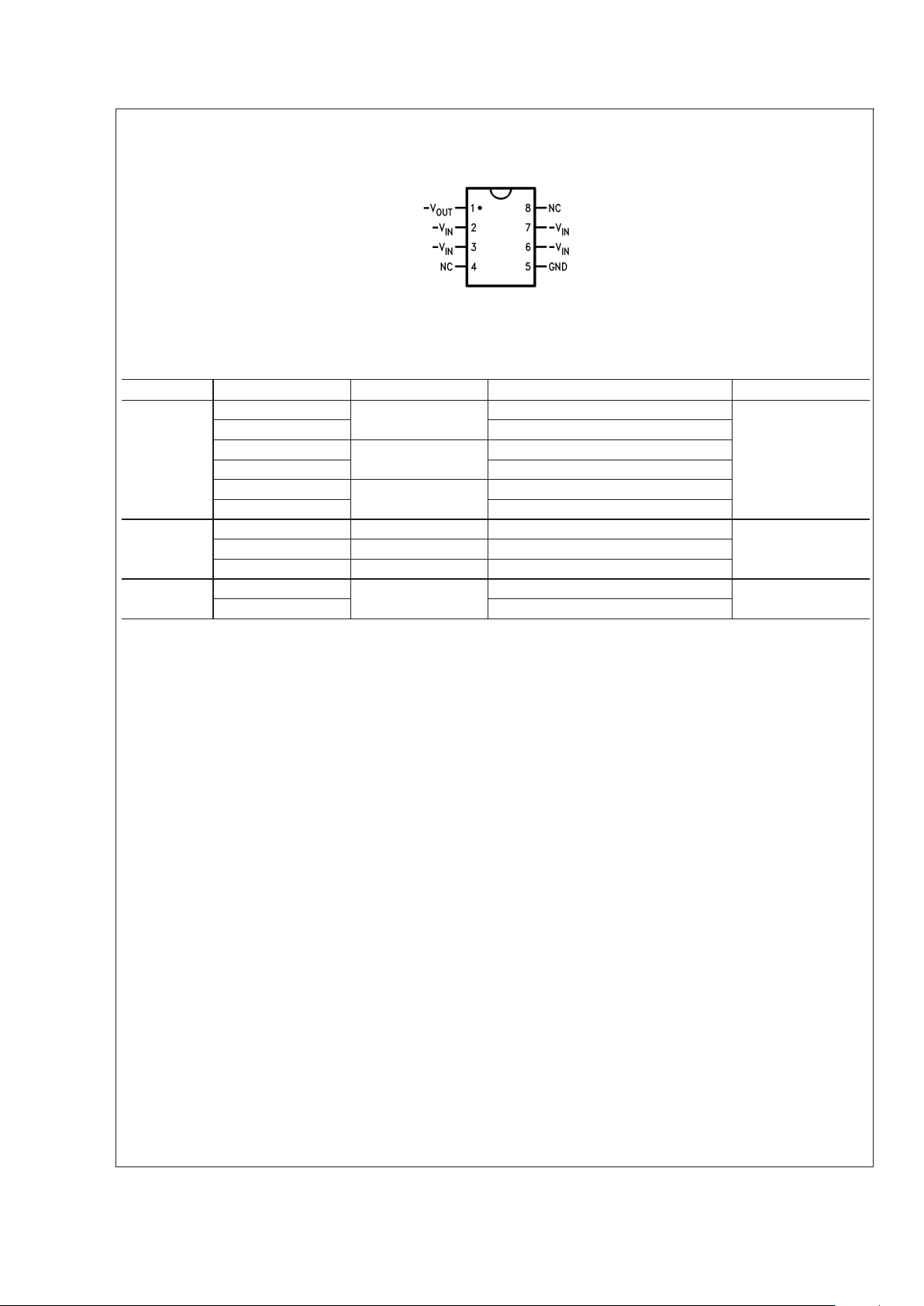
Connection Diagrams (Continued)
SO-8 Plastic (Narrow Body)
00774804
Top View
Ordering Information
Package Part Number Package Marking Transport Media NSC Drawing
8-Lead SOIC LM79L05ACM LM79L05ACM 95 Units/Rail M08A
LM79L05ACMX 2.5k Units Tape and Reel
LM79L13ACM LM79L12ACM 95 Units/Rail
LM79L13ACMX 2.5k Units Tape and Reel
LM79L15ACM LM79L15ACM 95 Units/Rail
LM79L15ACMX 2.5k Units Tape and Reel
3-Pin TO-92 LM13121Z-5.0 320L79L05 1800 Units Per Box Z03A
LM13121Z-12 320L79L12 1800 Units Per Box
LM13121Z-15 320L79L15 1800 Units Per Box
6-Bump
micro SMD
LM79L05ACTL XTPB 250 Units Tape and Reel TLA06AMA
LM79L05ACTLX 3k Units Tape and Reel
LM320L/LM79LXXAC/LM13121
www.national.com 2
Page 3
Absolute Maximum Ratings (Note 1)
If Military/Aerospace specified devices are required,
please contact the National Semiconductor Sales Office/
Distributors for availability and specifications.
Input Voltage
V
O
= −5V, −12V, −15V −35V
Internal Power Dissipation (Note 2) Internally Limited
Operating Temperature Range 0˚C to +70˚C
Maximum Junction Temperature +125˚C
Storage Temperature Range −55˚C to +150˚C
Lead Temperature
(Soldering, 10 sec.) 260˚C
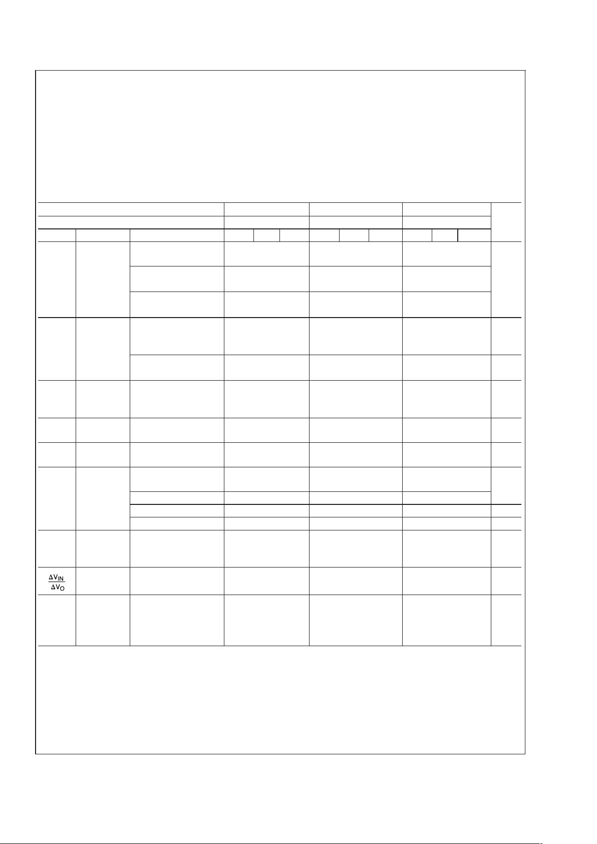
Electrical Characteristics (Note 3)
TA= 0˚C to +70˚C unless otherwise noted.
Output Voltage −5V −12V −15V
Input Voltage (unless otherwise noted) −10V −17V −20V Units
Symbol Parameter Conditions Min Typ Max Min Typ Max Min Typ Max
V
O
Output
Voltage
TJ= 25˚C, IO= 100mA −5.2 −5 −4.8 −12.5 −12 −11.5 −15.6 −15 −14.4
1mA ≤ IO≤ 100mA −5.25 −4.75 −12.6 −11.4 −15.75 −14.25
V
MIN
≤ VIN≤ V
MAX
(−20 ≤ VIN≤ −7.5) (−27 ≤ VIN≤ −14.8) (−30 ≤ VIN≤ −18) V
1mA ≤ I
O
≤ 40mA −5.25 −4.75 −12.6 −11.4 −15.75 −14.25
V
MIN
≤ VIN≤ V
MAX
(−20 ≤ VIN≤ −7) (−27 ≤ VIN≤ −14.5) (−30 ≤ VIN≤ −17.5)
∆V
O
Line
Regulation
TJ= 25˚C, IO= 100mA 60 45 45 mV
V
MIN
≤ VIN≤ V
MAX
(−20 ≤ VIN≤ −7.3) (−27 ≤ VIN≤ −14.6) (−30 ≤ VIN≤ −17.7) V
T
J
= 25˚C, IO= 40mA 60 45 45 mV
V
MIN
≤ VIN≤ V
MAX
(−20 ≤ VIN≤ −7) (−27 ≤ VIN≤ −14.5) (−30 ≤ VIN≤ −17.5) V
∆V
O
Load
Regulation
TJ= 25˚C
50 100 125 mV
1mA ≤ IO≤ 100mA
∆V
O
Long Term
Stability
IO= 100mA 20 48 60 mV/khrs
I
Q
Quiescent
Current
IO= 100mA 2 6 2 6 2 6 mA
∆I
Q
Quiescent
Current
1mA ≤ IO≤ 100mA 0.3 0.3 0.3
Change 1mA ≤ IO≤ 40mA 0.1 0.1 0.1 mA
I
O
= 100mA 0.25 0.25 0.25 mA
V
MIN
≤ VIN≤ V
MAX
(−20 ≤ VIN≤ −7.5) (−27 ≤ VIN≤ −14.8) (−30 ≤ VIN≤ −18) V
V
n
Output Noise
Voltage
TJ= 25˚C, IO= 100mA
40 96 120 µV
f = 10Hz − 10kHz
Ripple
Rejection
TJ= 25˚C, IO= 100mA
50 52 50 dB
f = 120Hz
Input Voltage T
J
= 25˚C, IO= 100mA −7.3 −14.6 −17.7 V
Required to I
O
= 40mA −7.0 −14.5 −17.5 V
Maintain Line
Regulation
Note 1: Absolute Maximum Ratings indicate limits beyond which damage to the device may occur. Operating Ratings indicate conditions for which the device is
functional, but do not guarantee specific performance limits.
Note 2: Thermal resistance of Z package is 60˚C/W θ
JC
, 232˚C/W θJAat still air, and 88˚C/W at 400 ft/min of air. The M package θJAis 180˚C/W in still air. The
maximum junction temperature shall not exceed 125˚C on electrical parameters.
Note 3: To ensure constant junction temperature, low duty cycle pulse testing is used.
LM320L/LM79LXXAC/LM13121
www.national.com3
Page 4

Typical Performance Characteristics
Maximum Average Power Dissipation (TO-92) Peak Output Current
00774811
00774812
Short Circuit Output Current Dropout Voltage
00774813
00774814
Ripple Rejection
Output Voltage vs. Temperature (Normalized to 1V
@
25˚C)
00774815
00774816
LM320L/LM79LXXAC/LM13121
www.national.com 4
Page 5

Typical Performance Characteristics (Continued)
Quiescent Current Output Impedance
00774817 00774818
Typical Applications
±
15V, 100mA Dual Power Supply
00774806
LM320L/LM79LXXAC/LM13121
www.national.com5
Page 6

Schematic Diagrams
−5V
00774809
−12V and −15V
00774810
LM320L/LM79LXXAC/LM13121
www.national.com 6
Page 7

Physical Dimensions inches (millimeters)
unless otherwise noted
SOIC Package (M)
NS Package Number M08A
Molded Offset TO-92 (Z)
NS Package Number Z03A
LM320L/LM79LXXAC/LM13121
www.national.com7
Page 8

Physical Dimensions inches (millimeters) unless otherwise noted (Continued)
NOTES: UNLESS OTHERWISE SPECIFIED
1. EPOXY COATING.
2. 63Sn/67Pb EUTECTIC BUMP.
3. RECOMMEND NON-SOLDER MASK DEFINED LANDING PAD.
4. PIN A1 ESTABLISHED BY LOWER LEFT CORNER WITH RESPECT TO TEXT ORIENTATION.
5. XXX IN DRAWING NUMBER REPRESENTS PACKAGE SIZE VARIATION WHERE X1 IS PACKAGE WIDTH, X2 IS PACKAGE LENGTH AND X3 IS
PACKAGE HEIGHT.
6. REFERENCE JEEC REGISTRATION MO-211, VARIATION BC.
6-Bump micro SMD
NS Package Number TLA06AMA
X
1
= 1006µm X2= 1793µm X3= 600µm
LIFE SUPPORT POLICY
NATIONAL’S PRODUCTS ARE NOT AUTHORIZED FOR USE AS CRITICAL COMPONENTS IN LIFE SUPPORT
DEVICES OR SYSTEMS WITHOUT THE EXPRESS WRITTEN APPROVAL OF THE PRESIDENT AND GENERAL
COUNSEL OF NATIONAL SEMICONDUCTOR CORPORATION. As used herein:
1. Life support devices or systems are devices or
systems which, (a) are intended for surgical implant
into the body, or (b) support or sustain life, and
whose failure to perform when properly used in
accordance with instructions for use provided in the
labeling, can be reasonably expected to result in a
significant injury to the user.
2. A critical component is any component of a life
support device or system whose failure to perform
can be reasonably expected to cause the failure of
the life support device or system, or to affect its
safety or effectiveness.
National Semiconductor
Americas Customer
Support Center
Email: new.feedback@nsc.com
Tel: 1-800-272-9959
National Semiconductor
Europe Customer Support Center
Fax: +49 (0) 180-530 85 86
Email: europe.support@nsc.com
Deutsch Tel: +49 (0) 69 9508 6208
English Tel: +44 (0) 870 24 0 2171
Français Tel: +33 (0) 1 41 91 8790
National Semiconductor
Asia Pacific Customer
Support Center
Fax: 65-6250 4466
Email: ap.support@nsc.com
Tel: 65-6254 4466
National Semiconductor
Japan Customer Support Center
Fax: 81-3-5639-7507
Email: nsj.crc@jksmtp.nsc.com
Tel: 81-3-5639-7560
www.national.com
LM320L/LM79LXXAC/LM13121 Series 3-Terminal Negative Regulators
National does not assume any responsibility for use of any circuitry described, no circuit patent licenses are implied and National reserves the right at any time without notice to change said circuitry and specifications.
 Loading...