

Page 1
LM341/LM78MXX Series
3-Terminal Positive Voltage Regulators
LM341/LM78MXX Series 3-Terminal Positive Voltage Regulators
July 1999
General Description
The LM341 and LM78MXX series of three-terminal positive
voltage regulators employ built-in current limiting, thermal
shutdown, and safe-operating area protection which makes
them virtually immune to damage from output overloads.
With adequate heatsinking, they can deliver in excess of
0.5A output current. Typical applications would include local
(on-card) regulators which can eliminate the noise and degraded performance associated with single-point regulation.
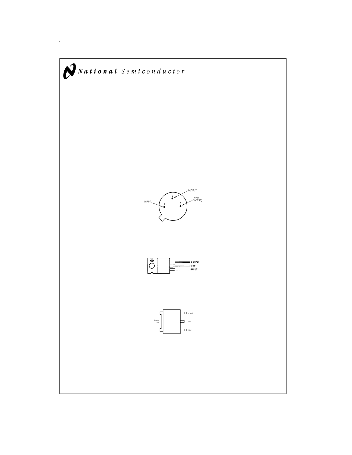
Connection Diagrams
TO-39 Metal Can Package (H)
Bottom View
Order Number LM78M05CH, LM78M12CH or LM78M15CH
See NS Package Number H03A
TO-220 Power Package (T)
Order Number LM341T-5.0, LM341T-12, LM341T-15, LM78M05CT, LM78M12CT or LM78M15CT
See NS Package Number T03B
Features
n Output current in excess of 0.5A
n No external components
n Internal thermal overload protection
n Internal short circuit current-limiting
n Output transistor safe-area compensation
n Available in TO-220, TO-39, and TO-252 D-PAK
packages
n Output voltages of 5V, 12V, and 15V
DS010484-5
DS010484-6
Top View
TO-252
DS010484-19
Order Number LM78M05CDT
See NS Package Number TD03B
© 1999 National Semiconductor Corporation DS010484 www.national.com
Top View
Page 2
Absolute Maximum Ratings (Note 1)
If Military/Aerospace specified devices are required,
please contact the National Semiconductor Sales Office/
Distributors for availability and specifications.
Lead Temperature (Soldering, 10 seconds)
TO-39 Package (H) 300˚C
TO-220 Package (T) 260˚C
Storage Temperature Range −65˚C to +150˚C
Operating Junction Temperature
Range −40˚C to +125˚C
Power Dissipation (Note 2) Internally Limited
Input Voltage
≤ 15V 35V
5V ≤ V
O
ESD Susceptibility TBD
Electrical Characteristics
Limits in standard typeface are for T
range. Limits are guaranteed by production testing or correlation techniques using standard Statistical Quality Control (SQC)
methods.
=
25˚C, and limits in boldface type apply over the −40˚C to +125˚C operating temperature
J
LM341-5.0, LM78M05C
Unless otherwise specified: V
=
IN
Symbol Parameter Conditions Min Typ Max Units
V
O
V
R LINE
V
R LOAD
I
Q
∆I
V
n
Q
Output Voltage I
Line Regulation 7.2V ≤ VIN≤ 25V I
Load Regulation 5 mA ≤ IL≤ 500 mA 100
Quiescent Current I
Quiescent Current Change 5 mA ≤ IL≤ 500 mA 0.5
Output Noise Voltage f=10 Hz to 100 kHz 40 µV
Ripple Rejection f=120 Hz, I
10V, C
=
IN
0.33 µF, C
=
0.1 µF
O
=
500 mA 4.8 5.0 5.2 V
L
5mA≤I
P
L
7.5V ≤ V
≤500 mA 4.75 5.0 5.25
L
≤ 7.5W, 7.5V ≤ VIN≤ 20V
D
=
500 mA 4 10.0 mA
≤ 25V, I
IN
=
500 mA
L
=
100 mA 50 mV
L
=
I
500 mA 100
L
=
500 mA 1.0
L
78 dB
V
IN
Input Voltage Required I
=
500 mA 7.2 V
L
to Maintain Line Regulation
∆V
O
www.national.com 2
Long Term Stability I
=
500 mA 20 mV/khrs
L
Page 3
Electrical Characteristics
Limits in standard typeface are for T
range. Limits are guaranteed by production testing or correlation techniques using standard Statistical Quality Control (SQC)
methods. (Continued)
=
25˚C, and limits in boldface type apply over the −40˚C to +125˚C operating temperature
J
LM341-12, LM78M12C
Unless otherwise specified: V
=
IN
Symbol Parameter Conditions Min Typ Max Units
V
O
V
R LINE
V
R LOAD
I
Q
∆I
V
n
Q
Output Voltage I
Line Regulation 14.5V ≤ VIN≤ 30V I
Load Regulation 5 mA ≤ IL≤ 500 mA 240
Quiescent Current I
Quiescent Current Change 5 mA ≤ IL≤ 500 mA 0.5
Output Noise Voltage f=10 Hz to 100 kHz 75 µV
Ripple Rejection f=120 Hz, I
19V, C
=
IN
0.33 µF, C
=
0.1 µF
O
=
500 mA 11.5 12 12.5 V
L
5mA≤I
P
L
14.8V ≤ V
≤500 mA 11.4 12 12.6
L
≤ 7.5W, 14.8V ≤ VIN≤ 27V
D
=
500 mA 4 10.0 mA
≤ 30V, I
IN
=
500 mA
L
=
100 mA 120 mV
L
=
I
500 mA 240
L
=
500 mA 1.0
L
71 dB
V
IN
Input Voltage Required I
=
500 mA 14.5 V
L
to Maintain Line Regulation
∆V
O
Long Term Stability I
=
500 mA 48 mV/khrs
L
LM341-15, LM78M15C
Unless otherwise specified: V
=
IN
Symbol Parameter Conditions Min Typ Max Units
V
O
V
R LINE
V
R LOAD
I
Q
∆I
V
n
Q
Output Voltage I
Line Regulation 17.6V ≤ VIN≤ 30V I
Load Regulation 5 mA ≤ IL≤ 500 mA 300
Quiescent Current I
Quiescent Current Change 5 mA ≤ IL≤ 500 mA 0.5
Output Noise Voltage f=10 Hz to 100 kHz 90 µV
Ripple Rejection f=120 Hz, I
V
IN
Input Voltage Required I
to Maintain Line Regulation
∆V
O
Note 1: Absolute maximum ratings indicate limits beyond which damage to the component may occur. Electrical specificationsdonotapplywhenoperating the device outside of its rated operating conditions.
Note 2: The typical thermal resistance of the three package types is:
Long Term Stability I
T (TO-220) package: θ
H (TO-39) package: θ
DT (TO-252) package: θ
(JA)
(JA)
=
60 ˚C/W, θ
=
120 ˚C/W, θ
=
(JA)
92 ˚C/W, θ
23V, C
(JC)
(JC)
(JC)
IN
=
5 ˚C/W
=
18 ˚C/W
=
=
0.33 µF, C
=
500 mA 14.4 15 15.6 V
L
5mA≤I
P
≤ 7.5W, 18V ≤ VIN≤ 30V
D
=
500 mA 4 10.0 mA
L
18V ≤ V
=
500 mA 17.6 V
L
=
500 mA 60 mV/khrs
L
10 ˚C/W
=
0.1 µF
O
≤500 mA 14.25 15 15.75
L
=
100 mA 150 mV
L
=
I
500 mA 300
L
L
=
500 mA 1.0
L
=
500 mA
69 dB
≤ 30V, I
IN
www.national.com3
Page 4
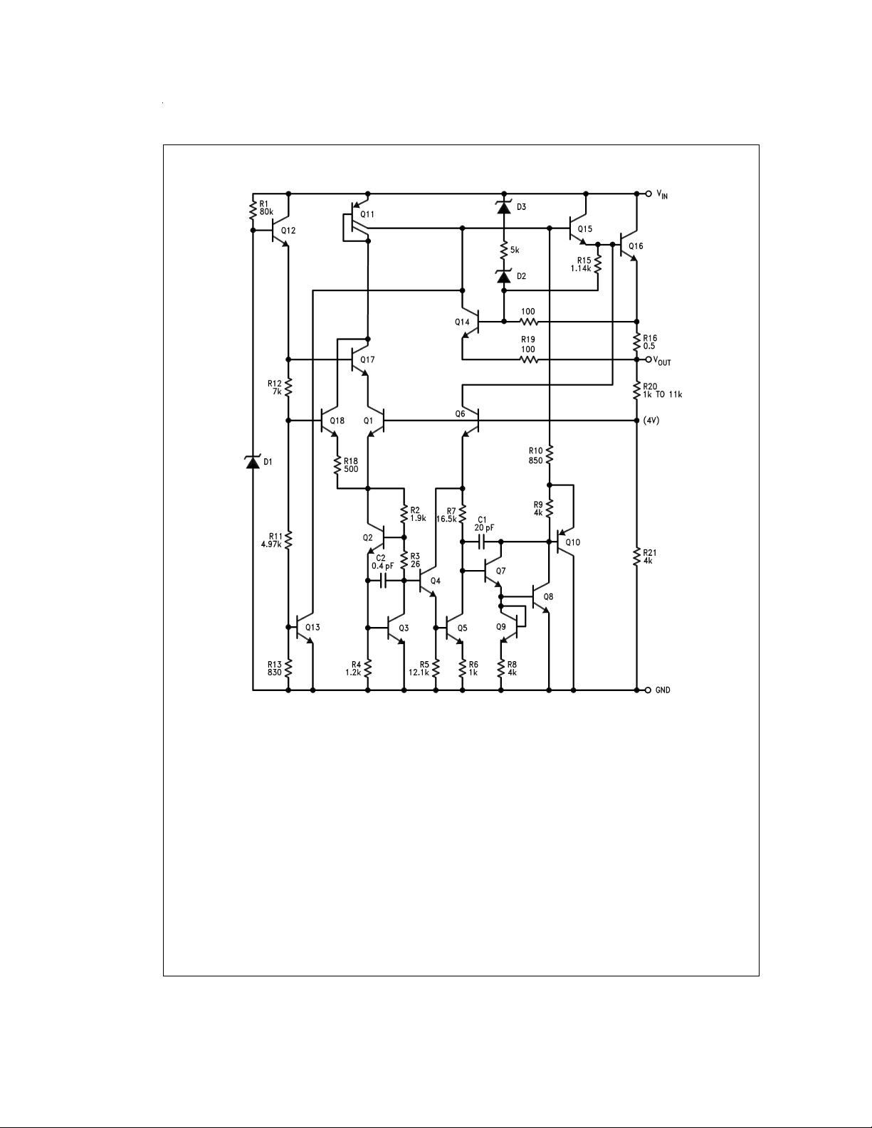
Schematic Diagram
www.national.com 4
DS010484-1
Page 5

Typical Performance Characteristics
Peak Output Current
Ripple Rejection
DS010484-10
Ripple Rejection
DS010484-11
Dropout Voltage
Output Voltage (Normalized
to 1V at T
=
25˚C)
J
DS010484-12
DS010484-14
DS010484-13
Quiescent Current
DS010484-15
www.national.com5
Page 6

Typical Performance Characteristics (Continued)
Quiescent Current
Line Transient Response
DS010484-16
Output Impedance
DS010484-17
Load Transient Response
DS010484-7
Design Considerations
The LM78MXX/LM341XX fixed voltage regulator series has
built-in thermal overload protection which prevents the device from being damaged due to excessive junction temperature.
The regulators also contain internal short-circuit protection
which limits the maximum output current, and safe-area protection for the pass transistor which reduces the short-circuit
current as the voltage across the pass transistor is increased.
Although the internal power dissipation is automatically limited, the maximum junction temperature of the device must
be kept below +125˚C in order to meet data sheet specifications. An adequate heatsink should be provided to assure
this limit is not exceeded under worst-case operating conditions (maximum input voltage and load current) if reliable
performance is to be obtained).
1.0 Heatsink Considerations
When an integrated circuit operates with appreciable current, its junction temperature is elevated. It is important to
quantify its thermal limits in order to achieve acceptable performance and reliability. This limit is determined by summing
the individual parts consisting of a series of temperature
rises from the semiconductor junction to the operating environment. A one-dimension steady-state model of conduction
heat transfer is demonstrated in The heat generated at the
www.national.com 6
DS010484-8
device junction flows through the die to the die attach pad,
through the lead frame to the surrounding case material, to
the printed circuit board, and eventually to the ambient environment. Below is a list of variables that may affect the thermal resistance and in turn the need for a heatsink.
θJC
R
(Component Variables) R
θCA
(Application Variables)
Leadframe Size & Material Mounting Pad Size, Material,
& Location
No. of Conduction Pins Placement of Mounting Pad
Die Size PCB Size & Material
Die Attach Material Traces Length & Width
Molding Compound Size and
Adjacent Heat Sources
Material
Volume of Air
Air Flow
Ambient Temperature
Shape of Mounting Pad
Page 7

Design Considerations (Continued)
DS010484-23
FIGURE 1. Cross-sectional view of Integrated Circuit
Mounted on a printed circuit board. Note that the case
temperature is measured at the point where the leads
contact with the mounting pad surface
The LM78MXX/LM341XX regulators have internal thermal
shutdown to protect the device from over-heating. Under all
possible operating conditions, the junction temperature of
the LM78MXX/LM341XX must be within the range of 0˚C to
125˚C. A heatsink may be required depending on the maximum power dissipation and maximum ambient temperature
of the application. To determine if a heatsink is needed, the
power dissipated by the regulator, P
=
I
I
IN
L+IG
=
P
(V
D
IN−VOUT)IL+VINIG
, must be calculated:
D
shows the voltages and currents which are present in the
circuit.
FIGURE 2. Power Dissipation Diagram
The next parameter which must be calculated is the maximum allowable temperature rise, T
=
θ
TR (max)/P
JA
If the maximum allowable value for θJA˚C/w is found to be
≥60˚C/W for TO-220 package or ≥92˚C/W for TO-252 package, no heatsink is needed since the package alone will dissipate enough heat to satisfy these requirements. If the calculated value for θ
required.
As a design aid,
TO-252 for different heatsink area. The copper patterns that
we used to measure these θ
Application Note Section. reflects the same test results as
what are in the
shows the maximum allowable power dissipation vs. ambient temperature for theTO-252 device. shows the maximum
allowable power dissipation vs. copper area (in
TO-252 device. Please see AN1028 for power enhancement
techniques to be used with TO-252 package.
TABLE 1. θ
Different Heatsink Area
JA
Layout Copper Area Thermal Resistance
Top Sice (in
2
)* Bottom Side (in2)(θJA, ˚C/W) TO-252
1 0.0123 0 103
2 0.066 0 87
3 0.3 0 60
4 0.53 0 54
5 0.76 0 52
61047
7 0 0.2 84
8 0 0.4 70
9 0 0.6 63
10 0 0.8 57
11 0 1 57
12 0.066 0.066 89
13 0.175 0.175 72
14 0.284 0.284 61
15 0.392 0.392 55
16 0.5 0.5 53
*
Tab of device attached to topside copper
(max):
R
D
fall below these limits, a heatsink is
JA
Table 1
shows the value of the θJAof
are shown at the end of the
JA
Table 1
DS010484-24
2
) for the
www.national.com7
Page 8

Design Considerations (Continued)
DS010484-20
FIGURE 3. θJAvs. 2oz Copper Area for TO-252
DS010484-21
FIGURE 5. Maximum Allowable Power Dissipation vs.
2oz. Copper Area for TO-252
Typical Application
DS010484-22
FIGURE 4. Maximum Allowable Power Dissipation vs.
Ambient Temperature for TO-252
www.national.com 8
*
Required if regulator input is more than 4 inches from input filter capacitor
(or if no input filter capacitor is used).
**
Optional for improved transient response.
DS010484-9
Page 9

Physical Dimensions inches (millimeters) unless otherwise noted
Order Number LM78M05CH, LM78M12CH or LM78M15CH
TO-39 Metal Can Package (H)
NS Package Number H03A
www.national.com9
Page 10

Physical Dimensions inches (millimeters) unless otherwise noted (Continued)
Order Number LM341T-5.0, LM341T-12, LM341T-15, LM78M05CT, LM78M12CT or LM78M15CT
TO-220 Power Package (T)
NS Package Number T03B
www.national.com 10
Page 11

Physical Dimensions inches (millimeters) unless otherwise noted (Continued)
LM341/LM78MXX Series 3-Terminal Positive Voltage Regulators
Order Number LM78M05CDT
TO-252
NS Package Number TD03B
LIFE SUPPORT POLICY
NATIONAL’S PRODUCTS ARE NOT AUTHORIZED FOR USE AS CRITICAL COMPONENTS IN LIFE SUPPORT
DEVICES OR SYSTEMS WITHOUT THE EXPRESS WRITTEN APPROVAL OF THE PRESIDENT AND GENERAL
COUNSEL OF NATIONAL SEMICONDUCTOR CORPORATION. As used herein:
1. Life support devices or systems are devices or
systems which, (a) are intended for surgical implant
into the body, or (b) support or sustain life, and
whose failure to perform when properly used in
accordance with instructions for use provided in the
2. A critical component is any component of a life
support device or system whose failure to perform
can be reasonably expected to cause the failure of
the life support device or system, or to affect its
safety or effectiveness.
labeling, can be reasonably expected to result in a
significant injury to the user.
National Semiconductor
Corporation
Americas
Tel: 1-800-272-9959
Fax: 1-800-737-7018
Email: support@nsc.com
www.national.com
National Semiconductor
Europe
Fax: +49 (0) 1 80-530 85 86
Email: europe.support@nsc.com
Deutsch Tel: +49 (0) 1 80-530 85 85
English Tel: +49 (0) 1 80-532 78 32
Français Tel: +49 (0) 1 80-532 93 58
Italiano Tel: +49 (0) 1 80-534 16 80
National Semiconductor
Asia Pacific Customer
Response Group
Tel: 65-2544466
Fax: 65-2504466
Email: sea.support@nsc.com
National Semiconductor
Japan Ltd.
Tel: 81-3-5639-7560
Fax: 81-3-5639-7507
National does not assume any responsibility for use of any circuitry described, no circuit patent licenses are implied and National reserves the right at any time without notice to change said circuitry and specifications.
 Loading...