

Page 1
LM759/LM77000
Power Operational Amplifiers
LM759/LM77000 Power Operational Amplifiers
November 1994
General Description
The LM759 and LM77000 are high performance operational
amplifiers that feature high output current capability. The
LM759 is capable of providing 325 mA and the LM77000
providing 250 mA. Both amplifiers feature small signal characteristics that are better than the LM741. The amplifiers
are designed to operate from a single or dual power supply
with an input common mode range that includes the negative supply. The high gain and high output power provide
superior performance. Internal current limiting, thermal shutdown, and safe area compensation are employed making
the LM759 and LM77000 essentially indestructible.
Features
Y
Output current
LM759Ð325 mA minimum
LM77000Ð250 mA minimum
Y
Internal short circuit current limiting
Y
Internal thermal overload protection
Y
Internal output transistors safe-area protection
Y
Input common mode voltage range includes ground or
negative supply
Applications
Y
Voltage regulators
Y
Audio amplifiers
Y
Servo amplifiers
Y
Power drivers
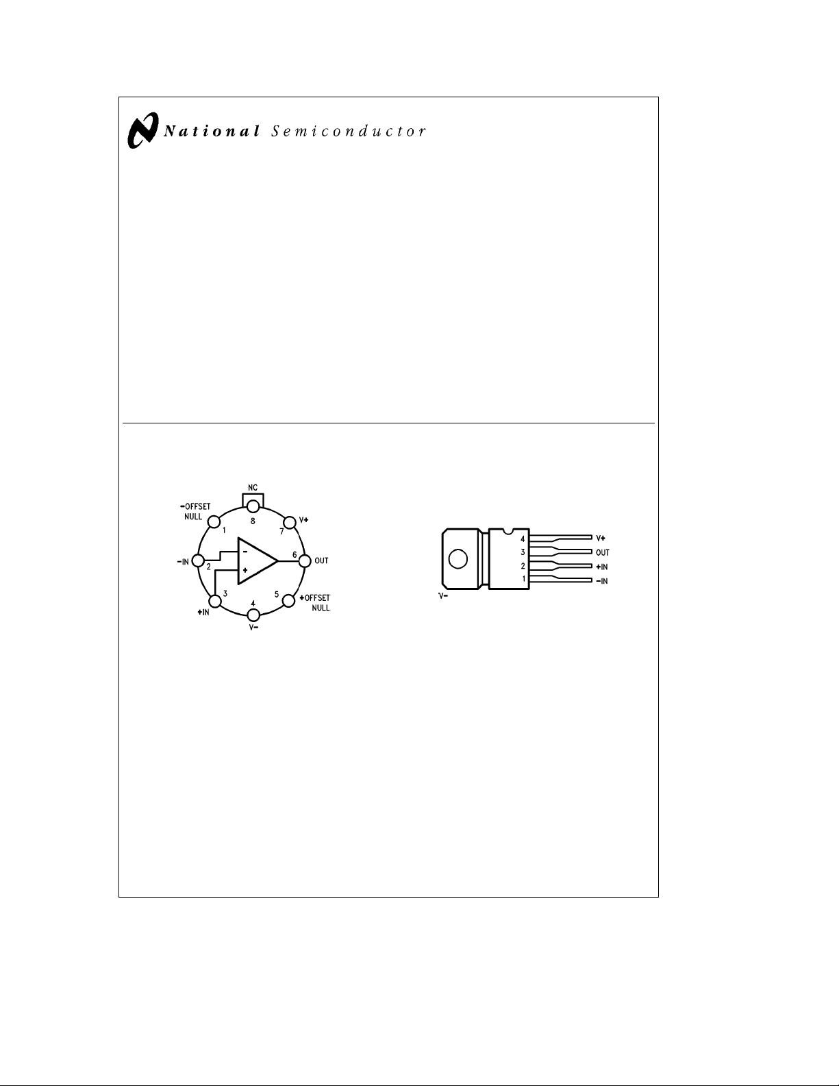
Connection Diagrams and Ordering Information
Lead 4 connected to case.
TL/H/10075– 1
Top View
Order Number LM759MH, LM759CH or LM759H/883
See NS Package Number H08C
Order Number LM759CP or LM77000CP
See NS Package Number P04A
Top View
TL/H/10075– 2
C
1995 National Semiconductor Corporation RRD-B30M115/Printed in U. S. A.
TL/H/10075
Page 2
Absolute Maximum Ratings
If Military/Aerospace specified devices are required,
please contact the National Semiconductor Sales
Office/Distributors for availability and specifications.
Storage Temperature Range
Metal Can
Plastic Package
Operating Junction Temperature Range
Military (LM759M)
Commercial (LM759C, LM77000C) 0
b
65§Ctoa175§C
b
65§Ctoa150§C
b
55§Ctoa150§C
Ctoa125§C
§
Lead Temperature
Metal Can (soldering, 60 sec) 300
Plastic Package (soldering, 10 sec) 265
§
§
Internal Power Dissipation (Note 1) Internally Limited
Supply Voltage
Differential Input Voltage 30V
Input Voltage (note 2)
C
C
g
18V
g
15V
LM759
Electrical Characteristics
e
T
25§C, V
J
Symbol Parameter Conditions Min Typ Max Units
V
IO
I
IO
I
IB
Z
I
I
CC
V
IR
I
OS
I
O PEAK
A
VS
TR Transient Response Rise Time R
Input Offset Voltage R
S
Input Offset Current 5.0 30 nA
Input Bias Current 50 150 nA
Input Impedance 0.25 1.5 MX
Supply Current 12 18 mA
Input Voltage Range V
Output Short Circuit Current
VCC–V
l
Peak Output Current 3.0V
Large Signal Voltage Gain R
L
L
Overshoot 5.0 %
SR Slew Rate R
BW Bandwidth A
The following specifications apply forb55§CsT
V
IO
I
IO
I
IB
Input Offset Voltage R
Input Offset Current 60 nA
Input Bias Current 300 nA
CMRR Common Mode Rejection Ratio R
PSRR Power Supply Rejection Ratio R
A
VS
V
OP
Large Signal Voltage Gain R
Output Voltage Swing R
L
V
s
J
S
S
S
L
L
e
g
15V, unless otherwise specified
CC
s
10 kX 1.0 3.0 mV
a
b
2V to VbV
e
30V
l
O
s
VCC–V
l
t
50X,V
e
50X,A
e
50X,A
e
1.0 1.0 MHz
a
150§C
s
10 kX 4.5 mV
s
10 kX 80 100 dB
s
10 kX 80 100 dB
t
50X,V
e
50X
s
10V
l
O
e
g
10V 50 200 V/mV
O
e
1.0 300 ns
V
e
1.0 0.6 V/ms
V
e
g
10V 25 200 V/mV
O
g
325
g
10
a
b
b
2V to V
g
200 mA
g
500 mA
g
12.5 V
V
2
Page 3
LM759C
Electrical Characteristics
e
T
25§C, V
J
Symbol Parameter Conditions Min Typ Max Units
V
IO
I
IO
I
IB
Z
I
I
CC
V
IR
I
OS
I
O PEAK
A
VS
TR Transient Response Rise Time R
Input Offset Voltage R
S
Input Offset Current 5.0 50 nA
Input Bias Current 50 250 nA
Input Impedance 0.25 1.5 MX
Supply Current 12 18 mA
Input Voltage Range V
Output Short Circuit Current
VCC–V
l
Peak Output Current 3.0V
Large Signal Voltage Gain R
L
L
Overshoot 10 %
SR Slew Rate R
BW Bandwidth A
The following specifications apply for 0
V
IO
I
IO
I
IB
Input Offset Voltage R
Input Offset Current 100 nA
Input Bias Current 400 nA
s
§
CMRR Common Mode Rejection Ratio R
PSRR Power Supply Rejection Ratio R
A
VS
V
OP
Large Signal Voltage Gain R
Output Voltage Swing R
L
V
s
a
T
125§C
J
S
S
S
L
L
e
g
15V, unless otherwise specified
CC
s
10 kX 1.0 6.0 mV
a
b
2V to VbV
e
30V
l
O
s
VCC–V
l
t
50X,V
e
50X,A
e
50X,A
e
1.0 1.0 MHz
s
10 kX 7.5 mV
s
10 kX 70 100 dB
s
10 kX 80 100 dB
t
50X,V
e
50X
s
10V
l
O
e
g
10V 25 200 V/mV
O
e
1.0 300 ns
V
e
1.0 0.5 V/ms
V
e
g
10V 25 200 V/mV
O
g
325
g
10
a
b
b
2V to V
g
200 mA
g
500 mA
g
12.5 V
V
3
Page 4
LM77000
Electrical Characteristics
e
T
25§C, V
J
Symbol Parameter Conditions Min Typ Max Units
V
IO
I
IO
I
IB
Z
I
I
CC
V
IR
I
OS
I
O PEAK
A
VS
Input Offset Voltage R
Input Offset Current 5.0 50 nA
Input Bias Current 50 250 nA
Input Impedance 0.25 1.5 MX
Supply Current 12 18 mA
Input Voltage Range
Output Short Circuit Current
Peak Output Current 3.0V
Large Signal Voltage Gain R
TR Transient Response Rise Time R
Overshoot 10 %
SR Slew Rate R
BW Bandwidth A
s
s
The following specifications apply for 0
V
IO
I
IO
I
IB
Input Offset Voltage R
Input Offset Current 100 nA
Input Bias Current 400 nA
a
T
§
125§C
J
CMR Common Mode Rejection R
PSRR Power Supply Rejection Ratio R
A
VS
V
OP
Note 1: Although the internal power dissipation is limited, the junction temperature must be kept below the maximum specified temperature in order to meet data
sheet specifications. To calculate the maximum junction temperature or heat sink required, use the thermal resistance values which follow the Equivalent Circuit
Schematic.
Note 2: For a supply voltage less than 30V between V
Note 3: For military electrical specifications RETS759X are available for LM759H.
Large Signal Voltage Gain R
Output Voltage Swing R
a
and Vb, the absolute maximum input voltage is equal to the supply voltage.
e
g
15V, unless otherwise specified
CC
s
10 kX 1.0 8.0 mV
S
b
a
13 to V
VCC–V
l
e
30V
l
O
s
VCC–V
l
t
50X,V
L
e
50X,A
L
e
50X,A
L
e
1.0 1.0 MHz
V
s
10 kX 10 mV
S
s
10 kX 70 100 dB
S
s
10 kX 80 100 dB
S
t
50X,V
L
e
50X
L
s
10V
l
O
e
g
10V 25 200 V/mV
O
e
1.0 300 ns
V
e
1.0 0.5 V/ms
V
e
g
10V 25 200 V/mV
O
g
250
g
10
b
a
13 to V
g
200 mA
g
400 mA
g
12.5 V
V
4
Page 5
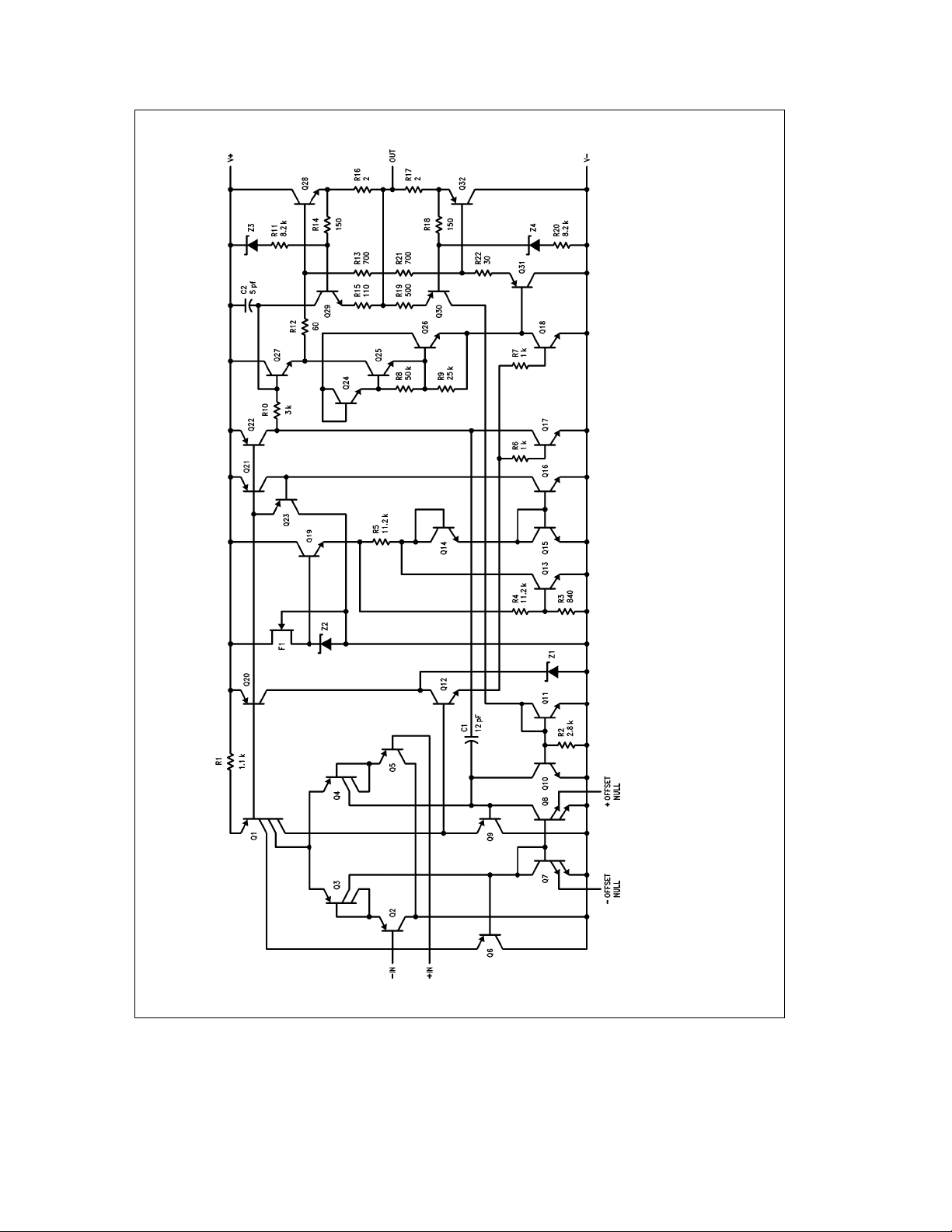
Equivalent Circuit
TL/H/10075– 3
Note: All resistor values in ohms.
5
Page 6

Package i
§
i
JC
C/W§C/W§C/W§C/W
i
JC
JA
Plastic Package (P) 8.0 12 75 80
Metal Can (H) 30 40 120 150
Typ Max Typ Max
P
D Max
i
CA
T
e
T
e
e
i
CS
J Max
i
JC
J Max
a
T
A
or
a
i
CA
b
T
A
(without a heat sink)
i
JA
i
SA
b
Solving TJ:
e
T
J
Where:
T
J
T
A
P
D
i
JA
i
JC
i
CA
i
CS
i
SA
a
T
A
e
a
T
A
e
Junction Temperature
e
Ambient Temperature
e
Power Dissipation
e
Junction to ambient thermal resistance
e
Junction to case thermal resistance
e
Case to ambient thermal resistance
e
Case to heat sink thermal resistance
e
Heat sink to ambient thermal resistance
a
PD(i
iCA)or
JC
PDiJA(without a heat sink)
i
JA
Metal Can Package (LM759CH/LM759MH)
The LM759 in the 8-Lead TO-99 metal can package must
be used with a heat sink. With
g
15V power supplies, the
LM759 can dissipate up to 540 mW in its quiescent (no
load) state. This would result in a 100
ature to 125
order to avoid this problem, it is advisable to use either a slip
C (assuming a 25§C ambient temperature). In
§
C rise in chip temper-
§
on or stud mount heat sink with this package. If a stud
mount heat sink is used, it may be necessary to use insulating washers between the stud and the chassis because the
case of the LM759 is internally connected to the negative
power supply terminal.
Plastic Package (LM759CP/LM77000CP)
The LM759CP and LM77000CP are designed to be attached by the tab to a heat sink. This heat sink can be either
one of the many heat sinks which are commercially available, a piece of metal such as the equipment chassis, or a
suitable amount of copper foil as on a double sided PC
board. The important thing to remember is that the negative
power supply connection to the op amp must be made
through the tab. Furthermore, adequate heat sinking must
be provided to keep the chip temperature below 125
der worst case load and ambient temperature conditions.
C un-
§
Mounting Hints
6
Page 7

Typical Performance Characteristics
Frequency Response for
Various Closed Loop Gains
Output Voltage vs
Load Resistance
Total Harmonic Distortion
vs Frequency
Open Loop vs
Frequency Response
Voltage Follower Large
Signal Pulse Response
Total Harmonic Distortion
vs Power Output
Output Voltage
vs Frequency
Voltage Follower
Transient Response
Input Noise Voltage
vs Frequency
Noise Current
vs Frequency
Short Circuit Current
vs Junction Temperature
7
Peak Output Current
vs Output Voltage
TL/H/10075– 4
Page 8

Applications
Offset Null Circuit
Audio Applications
Low Cost Phono Amplifier
TL/H/10075– 5
Paralleling LM759 Power Op Amps
Speaker Output Min
Impedance Power Supply
(Ohms) (Watts) (Volts)
4 0.18 9 2.4
8 0.36 12 4.8
16 0.72 15 9.6
32 1.44 25 19.2
TL/H/10075– 6
V
O
P–P
(Volts)
TL/H/10075– 7
8
Page 9

Applications (Continued)
Bi-Directional Intercom System Using the LM759 Power Op Amp
Features:
Circuit Simplicity
1 Watt of Audio Output
Duplex operation with only one two-wire cable as interconnect.
Note 1: All resistor values in ohms.
TL/H/10075– 9
9
Page 10

Applications (Continued)
High Slew Rate Power Op Amp/Audio Amp
Features:
High Slew Rate 9 V/ms
High 3 dB Power Bandwidth 85 kHz
18 Watts Output Power into an 8X load.
Low DistortionÐ0.2%, 10 Vrms, 1 kHz into 8X
Design Consideration
t
10
A
V
Servo Applications
AG Servo AmplifierÐBridge Type
TL/H/10075– 10
TL/H/10075– 11
Features:
Gain of 10
Use of LM759 Means Simple Inexpensive Circuit
Design Considerations:
325 mA Max Output Current
DC Servo Amplifier
Features:
Circuit Simplicity
One Chip Means Excellent Reliability
Design Considerations
s
325 mA
I
O
Note 1: All resistor values in ohms.
10
TL/H/10075– 12
Page 11

Regulator Applications
Features:
Wide Output Voltage Range (
Excellent Load Regulation DV
Excellent Line Regulation DV
Note 1: All resistor values in ohms.
g
2.2V tog30V)
k
g
O
k
g
O
Adjustable Dual Tracking Regulator
e
5mVforDI
2mVforDV
g
0.2 A
O
e
10V
I
10 Amp Ð 12 Volt Regulator
TL/H/10075– 13
Features:
Excellent Load and Line Regulation
Excellent Temperature Coefficient-Depends
Largely on Tempco of the Reference Zener
Note 1: All resistor values in ohms.
TL/H/10075– 14
11
Page 12

12
Page 13

Physical Dimensions inches (millimeters)
Order Number LM759MH, LM759CH or LM759H/883
8-Lead Metal Package
NS Package Number H08C
13
Page 14

Physical Dimensions inches (millimeters) (Continued)
LM759/LM77000 Power Operational Amplifiers
Order Number LM759CP or LM77000CP
NS Package Number P04A
LIFE SUPPORT POLICY
NATIONAL’S PRODUCTS ARE NOT AUTHORIZED FOR USE AS CRITICAL COMPONENTS IN LIFE SUPPORT
DEVICES OR SYSTEMS WITHOUT THE EXPRESS WRITTEN APPROVAL OF THE PRESIDENT OF NATIONAL
SEMICONDUCTOR CORPORATION. As used herein:
1. Life support devices or systems are devices or 2. A critical component is any component of a life
systems which, (a) are intended for surgical implant support device or system whose failure to perform can
into the body, or (b) support or sustain life, and whose be reasonably expected to cause the failure of the life
failure to perform, when properly used in accordance support device or system, or to affect its safety or
with instructions for use provided in the labeling, can effectiveness.
be reasonably expected to result in a significant injury
to the user.
National Semiconductor National Semiconductor National Semiconductor National Semiconductor
Corporation Europe Hong Kong Ltd. Japan Ltd.
1111 West Bardin Road Fax: (
Arlington, TX 76017 Email: cnjwge@tevm2.nsc.com Ocean Centre, 5 Canton Rd. Fax: 81-043-299-2408
Tel: 1(800) 272-9959 Deutsch Tel: (
Fax: 1(800) 737-7018 English Tel: (
National does not assume any responsibility for use of any circuitry described, no circuit patent licenses are implied and National reserves the right at any time without notice to change said circuitry and specifications.
Fran3ais Tel: (
Italiano Tel: (
a
49) 0-180-530 85 86 13th Floor, Straight Block, Tel: 81-043-299-2309
a
49) 0-180-530 85 85 Tsimshatsui, Kowloon
a
49) 0-180-532 78 32 Hong Kong
a
49) 0-180-532 93 58 Tel: (852) 2737-1600
a
49) 0-180-534 16 80 Fax: (852) 2736-9960
 Loading...