

Page 1
LM748 Operational Amplifier
LM748 Operational Amplifier
November 1994
General Description
The LM748 is a general purpose operational amplifier with
external frequency compensation.
The unity-gain compensation specified makes the circuit
stable for all feedback configurations, even with capacitive
loads. It is possible to optimize compensation for best high
frequency performance at any gain. As a comparator, the
output can be clamped at any desired level to make it compatible with logic circuits.
The LM748C is specified for operation over the 0
a
70§C temperature range.
Cto
§
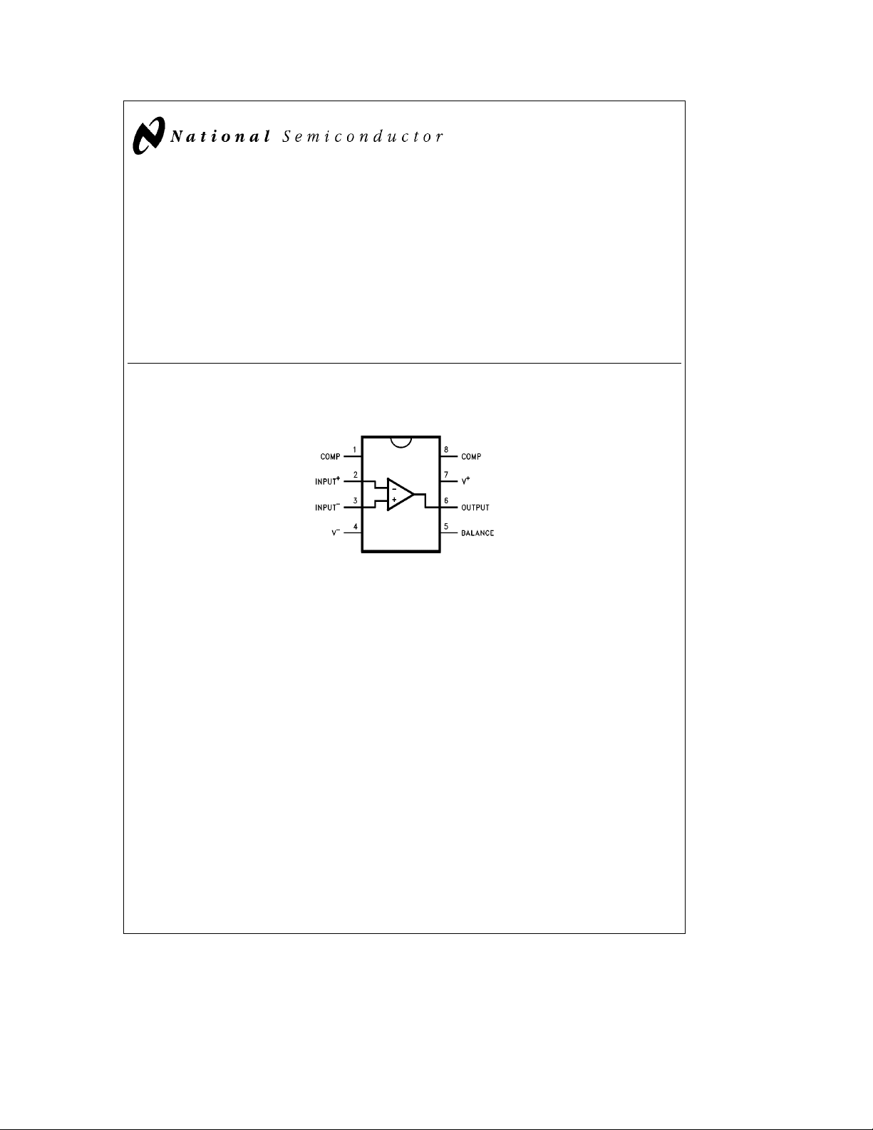
Connection Diagram
Dual-In-Line Package
Top View
Order Number LM748CN
See NS Package Number N08B
Features
Y
Frequency compensation with a single 30 pF capacitor
Y
Operation fromg5V tog20V
Y
Continuous short-circuit protection
Y
Operation as a comparator with differential inputs as
g
high as
Y
No latch-up when common mode range is exceeded
Y
Same pin configuration as the LM101
30V
TL/H/11478– 2
C
1995 National Semiconductor Corporation RRD-B30M115/Printed in U. S. A.
TL/H/11478
Page 2
Absolute Maximum Ratings
If Military/Aerospace specified devices are required,
please contact the National Semiconductor Sales
Office/Distributors for availability and specifications.
Supply Voltage
g
22V
Power Dissipation (Note 1) 500 mW
g
Differential Input Voltage
30V
Input Voltage (Note 2)
Output Short-Circuit Duration (Note 3)
Operating Temperature Range:
LM748C 0
Storage Temperature Range
Lead Temperature (Soldering, 10 sec.)
b
65§Ctoa150§C
g
Ctoa70C
§
a
300§C
15V
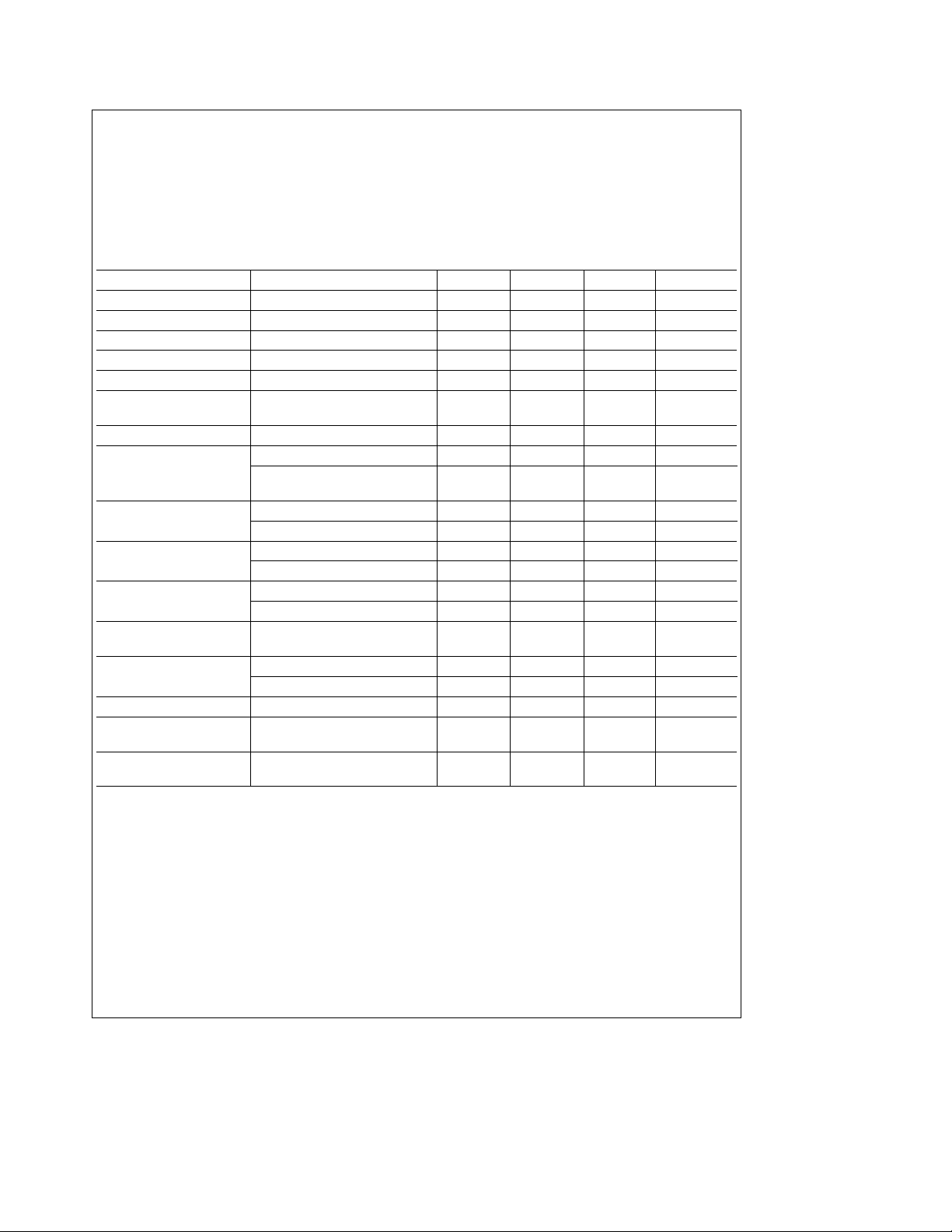
Electrical Characteristics (Note 4)
Parameter Conditions Min Typ Max Units
Input Offset Voltage T
Input Offset Current T
Input Bias Current T
Input Resistance T
Supply Current T
Large Signal T
Voltage Gain V
Input Offset Voltage R
Average Temperature R
Coefficient of Input
Offset Voltage
Input Offset Current T
Input Bias Current T
Supply Current T
Large Signal V
Voltage Gain R
Output Voltage V
Swing
Input Voltage Range V
Common-Mode R
Rejection Ratio
Supply Voltage R
Rejection Ratio
Note 1: For operating at elevated temperatures, the device must be derated based on a maximum junction to case thermal resistance of 45§C per watt, or 150§C
per watt junction to ambient. (See Curves).
Note 2: For supply voltages less than
Note 3: Continuous short circuit is allowed for case temperatures to
Note 4: These specifications apply for
e
A
e
A
e
A
e
A
e
A
e
A
OUT
s
S
s
S
s
R
S
e
A
eb
T
A
e
A
eb
T
A
ea
A
eb
T
A
e
S
t
2kX
L
e
S
e
V
S
e
S
s
10 kX
S
s
10 kX
S
g
15V, the absolute maximum input voltage is equal to the supply voltage.
s
g
5VsV
S
s
25§C, R
10 kX 1.0 5.0 mV
S
25§C 40 200 nA
25§C 120 500 nA
25§C 300 800 kX
e
g
10V, R
g
15V 1.8 2.8 mA
S
e
g
15V
S
t
2kX
L
50 160 V/mV
25§C, V
25§C, V
e
10 kX 6.0 mV
50X 3.0 mV/§C
10 kX
6.0 mV/
0§Ctoa70§C 300 nA
55§Ctoa125§C 500 nA
0§Ctoa70§C 0.8 mA
55§Ctoa125§C 1.5 mA
e
125§C, V
g
15V 1.2 2.25 mA
S
55§Ctoa125§C 1.9 3.3 mA
OUT
L
L
e
e
e
g
10 kX
2kX
10V
25 V/mV
g
12
g
10
g
12 V
g
14 V
g
13 V
g
15V, V
g
15V, R
g
15V, R
g
15V
70 90 dB
77 90 dB
a
125§C and ambient temperatures toa70§C.
a
15V and 0§CsT
s
a
70§C, unless otherwise specified.
A
C
§
2
Page 3

Typical Applications
Inverting Amplifier with Balancing Circuit
²
May be zero or equal to parallel TL/H/11478– 3
combination of R1 and R2 for minimum offset.
Voltage Comparator for Driving
RTL Logic or High Current Driver
Voltage Comparator for Driving
DTL or TTL Integrated Circuits
TL/H/11478– 4
TL/H/11478– 5
Guaranteed Performance Characteristics (Note 4)
Input Voltage Range Output Swing Voltage Gain
3
TL/H/11478– 6
Page 4

Typical Performance Characteristics
Supply Current Voltage Gain Input Bias Current
Current Limiting Input Current Dissipation
Open Loop
Frequency Response
Large Signal
Frequency Response
Maximum Power
Voltage Follower
Pulse Response
TL/H/11478– 7
4
Page 5

5
Page 6

Physical Dimensions inches (millimeters)
LM748 Operational Amplifier
Dual-In-Line Package (N)
Order Number LM748CN
NS Package Number N08E
LIFE SUPPORT POLICY
NATIONAL’S PRODUCTS ARE NOT AUTHORIZED FOR USE AS CRITICAL COMPONENTS IN LIFE SUPPORT
DEVICES OR SYSTEMS WITHOUT THE EXPRESS WRITTEN APPROVAL OF THE PRESIDENT OF NATIONAL
SEMICONDUCTOR CORPORATION. As used herein:
1. Life support devices or systems are devices or 2. A critical component is any component of a life
systems which, (a) are intended for surgical implant support device or system whose failure to perform can
into the body, or (b) support or sustain life, and whose be reasonably expected to cause the failure of the life
failure to perform, when properly used in accordance support device or system, or to affect its safety or
with instructions for use provided in the labeling, can effectiveness.
be reasonably expected to result in a significant injury
to the user.
National Semiconductor National Semiconductor National Semiconductor National Semiconductor
Corporation Europe Hong Kong Ltd. Japan Ltd.
1111 West Bardin Road Fax: (
Arlington, TX 76017 Email: cnjwge@tevm2.nsc.com Ocean Centre, 5 Canton Rd. Fax: 81-043-299-2408
Tel: 1(800) 272-9959 Deutsch Tel: (
Fax: 1(800) 737-7018 English Tel: (
National does not assume any responsibility for use of any circuitry described, no circuit patent licenses are implied and National reserves the right at any time without notice to change said circuitry and specifications.
Fran3ais Tel: (
Italiano Tel: (
a
49) 0-180-530 85 86 13th Floor, Straight Block, Tel: 81-043-299-2309
a
49) 0-180-530 85 85 Tsimshatsui, Kowloon
a
49) 0-180-532 78 32 Hong Kong
a
49) 0-180-532 93 58 Tel: (852) 2737-1600
a
49) 0-180-534 16 80 Fax: (852) 2736-9960
 Loading...