

Page 1
查询LM747供应商
LM747
Dual Operational Amplifier
LM747 Dual Operational Amplifier
November 1994
General Description
The LM747 is a general purpose dual operational amplifier.
The two amplifiers share a common bias network and power
supply leads. Otherwise, their operation is completely independent.
Additional features of the LM747 are: no latch-up when input common mode range is exceeded, freedom from oscillations, and package flexibility.
The LM747C/LM747E is identical to the LM747/LM747A
except that the LM747C/LM747E has its specifications
guaranteed over the temperature range from 0
instead of
b
55§Ctoa125§C.
Ctoa70§C
§
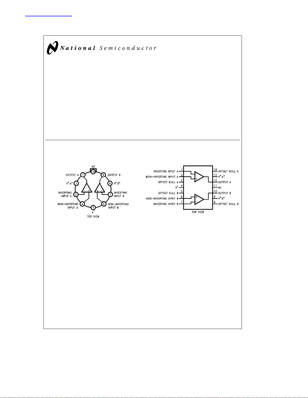
Connection Diagrams
Metal Can Package
TL/H/11479– 4
Order Number LM747H
See NS Package Number H10C
*VaA and VaB are internally connected.
Features
Y
No frequency compensation required
Y
Short-circuit protection
Y
Wide common-mode and differential voltage ranges
Y
Low power consumption
Y
No latch-up
Y
Balanced offset null
Dual-In-Line Package
Order Number LM747CN or LM747EN
See NS Package Number N14A
TL/H/11479– 5
C
1995 National Semiconductor Corporation RRD-B30M115/Printed in U. S. A.
TL/H/11479
Page 2
Absolute Maximum Ratings
If Military/Aerospace specified devices are required,
please contact the National Semiconductor Sales
Office/Distributors for availability and specifications.
Supply Voltage
LM747/LM747A
LM747C/LM747E
g
22V
g
18V
Power Dissipation (Note 1) 800 mW
Differential Input Voltage
g
30V
Input Voltage (Note 2)
Output Short-Circuit Duration Indefinite
Operating Temperature Range
LM747/LM747A
LM747C/LM747E 0
Storage Temperature Range
Lead Temperature (Soldering, 10 sec.) 300§C
Electrical Characteristics (Note 3)
Parameter Conditions
Input Offset Voltage T
e
25§C
A
s
R
10 kX 1.0 5.0 2.0 6.0
S
s
R
50X 0.8 3.0
S
s
R
50X 4.0
S
s
R
10 kX 6.0 7.5
S
Average Input Offset 15
Voltage Drift
Input Offset Voltage T
Adjustment Range
Input Offset Current T
e
A
e
A
e
25§C, V
g
20V
S
25§C 3.0 30 20 200 20 200
Average Input Offset
Current Drift
Input Bias Current T
Input Resistance T
Input Voltage Range T
Large Signal T
Voltage Gain V
Output Voltage Swing V
Output Short T
Circuit Current 10 40
Common-Mode R
Rejection Ratio
e
25§C 30 80 80 500 80 500 nA
A
s
T
V
V
R
V
V
V
R
R
V
R
R
R
AMIN
A
S
A
A
S
S
L
S
S
S
S
L
L
S
L
L
A
S
S
s
T
T
A
AMAX
e
e
e
e
e
e
t
e
e
e
e
t
t
e
t
t
e
s
s
e
25§C, V
g
20V 0.5
g
20V 1.0 6.0 0.3 2.0 0.3 2.0
S
25§C
t
25§C, R
g
g
2kX
g
g
g
g
20V, V
15V, V
20V, V
15V, V
5V, V
20V
2kX
L
e
g
15V 50 V/mV
O
e
g
10V 50 200 20 200
O
e
g
15V 32 V/mV
O
e
g
10V 25 15 V/mV
O
e
g
2V 10 V/mV
O
10 kX
2kX
g
15V
10 kX
2kX
25§C1025352525
e
CM
CM
g
e
g
10 kX,V
50 kX,V
LM747A/LM747E LM747 LM747C
Min Typ Max Min Typ Max Min Typ Max
g
10
0.5 nA/
0.210 1.5 0.8 mA
g12g
g
g
13
16
15
12V 70 90 70 90
12V 80 95
b
55§Ctoa125§C
Ctoa70§C
§
b
65§Ctoa150§C
g
15
g
15 mV
70 85 500 300
g12g
13
g12g
13
g12g
g10g
14
13
g12g
g10g
14
13
g
Units
mV/
V/mV
15V
mV
mV
nA
MX
mA
dB
C
§
C
§
V
V
V
2
Page 3
Electrical Characteristics (Note 3) (Continued)
Parameter Conditions
e
Supply Voltage V
Rejection Ratio R
Transient Response T
Rise Time 0.25 0.8 0.3 0.3 ms
g
20V to V
S
s
50X 86 96
S
s
10 kX 77 96 77 96
R
S
e
25§C, Unity Gain
A
e
g
S
Overshoot 6.0 20 5 5 %
Bandwidth (Note 4) T
Slew Rate T
Supply Current/Amp T
Power Consumption/Amp T
LM747A V
LM747E V
LM747 V
Note 1: The maximum junction temperature of the LM747C/LM747E is 100§C. For operating at elevated temperatures, devies in the TO-5 package must be
derated based on a thermal resistance of 150
W, junction to ambient.
Note 2: For supply voltages less than
Note 3: These specifications apply for
specified. The LM747 and LM747C are specified for V
Note 4: Calculated value from: 0.35/Rise Time (m s).
e
25§C 0.437 1.5 MHz
A
e
25§C, Unity Gain 0.3 0.7 0.5 0.5 V/ms
A
e
25§C 2.5 1.7 2.8 1.7 2.8 mA
A
e
25§C
A
e
g
20V 80 150
V
S
e
g
V
15V 50 85 50 85
S
e
g
20V
S
e
T
T
A
AMIN
e
T
T
A
AMAX
e
g
20V 150
S
e
T
T
A
AMIN
e
T
T
A
AMAX
e
g
15V
S
e
T
T
A
AMIN
e
T
T
A
AMAX
C/W, junction to ambient, or 45§C/W, junction to case. The thermal resistance of the dual-in-line package is 100§C/
§
g
15V, the absolute maximum input voltage is equal to the supply voltage.
s
g
5VsV
g
20V andb55§CsT
S
e
S
LM747A/LM747E LM747 LM747C
Min Typ Max Min Typ Max Min Typ Max
5V
165
135
150 mW
150
60 100
45 75
g
15V andb55§CsT
s
125§C for the LM747A and 0§CsT
A
s
125§C and 0§CsT
A
s
70§C for the LM747E unless otherwise
A
s
70§C, respectively, unless otherwise specified.
A
Units
dB
mW
mW
mW
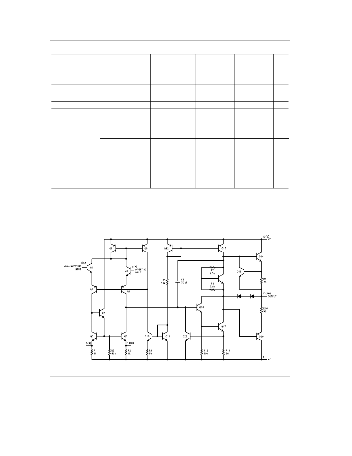
Schematic Diagram (Each Amplifier)
Note: Numbers in parentheses are pin numbers for amplifier B. DIP only.
TL/H/11479– 1
3
Page 4

Typical Performance Characteristics
Input Bias and Offset
Currents vs Ambient
Temperature
DC Parameters
vs Supply Voltage
Common Mode Rejection
Ratio vs Frequency
Output Voltage Swing
vs Frequency
Normalized DC Parameters
vs Ambient Temperature
Frequency Characteristics
vs Supply Voltage
Output Voltage Swing
vs Load Resistance
Transient Response vs Ambient Temperature
Output Resistance
vs Frequency
Output Swing and
Input Range vs
Supply Voltage
Frequency Characteristics
Open Loop Transfer
Characteristics vs Frequency
TL/H/11479– 2
4
Page 5

Typical Performance Characteristics (Continued)
Input Resistance and
Input Capacitance
vs Frequency
Input Noise Voltage
and Current
vs Frequency
Broadband Noise for
Various Bandwidths
Voltage Follower Large
Signal Pulse Response
TL/H/11479– 3
5
Page 6

6
Page 7

Physical Dimensions inches (millimeters)
Metal Can Package (H)
Order Number LM747H
NS Package Number H10C
7
Page 8

Physical Dimensions inches (millimeters) (Continued)
LM747 Dual Operational Amplifier
Dual-In-Line Package (N)
Order Number LM747CN or LM747EN
NS Package Number N14A
LIFE SUPPORT POLICY
NATIONAL’S PRODUCTS ARE NOT AUTHORIZED FOR USE AS CRITICAL COMPONENTS IN LIFE SUPPORT
DEVICES OR SYSTEMS WITHOUT THE EXPRESS WRITTEN APPROVAL OF THE PRESIDENT OF NATIONAL
SEMICONDUCTOR CORPORATION. As used herein:
1. Life support devices or systems are devices or 2. A critical component is any component of a life
systems which, (a) are intended for surgical implant support device or system whose failure to perform can
into the body, or (b) support or sustain life, and whose be reasonably expected to cause the failure of the life
failure to perform, when properly used in accordance support device or system, or to affect its safety or
with instructions for use provided in the labeling, can effectiveness.
be reasonably expected to result in a significant injury
to the user.
National Semiconductor National Semiconductor National Semiconductor National Semiconductor
Corporation Europe Hong Kong Ltd. Japan Ltd.
1111 West Bardin Road Fax: (
Arlington, TX 76017 Email: cnjwge@tevm2.nsc.com Ocean Centre, 5 Canton Rd. Fax: 81-043-299-2408
Tel: 1(800) 272-9959 Deutsch Tel: (
Fax: 1(800) 737-7018 English Tel: (
National does not assume any responsibility for use of any circuitry described, no circuit patent licenses are implied and National reserves the right at any time without notice to change said circuitry and specifications.
Fran3ais Tel: (
Italiano Tel: (
a
49) 0-180-530 85 86 13th Floor, Straight Block, Tel: 81-043-299-2309
a
49) 0-180-530 85 85 Tsimshatsui, Kowloon
a
49) 0-180-532 78 32 Hong Kong
a
49) 0-180-532 93 58 Tel: (852) 2737-1600
a
49) 0-180-534 16 80 Fax: (852) 2736-9960
 Loading...