

Page 1
HIGH PRECISION VOLTAGE REGULATOR
■ INPUTVOLTAGEUP TO 40V
■ OUTPUTVOLTAGEADJUSTABLE FROM2
TO 37V
■ POSITIVEOR NEGATIVESUPPLY
OPERATION
■ SERIES,SHUNT, SWITCHINGOR
FLOATING OPERATION
■ OUTPUTCURRENT TO150mAWITHOUT
EXTERNALPASS TRANSISTOR
■ ADJUSTABLECURRENT LIMITING
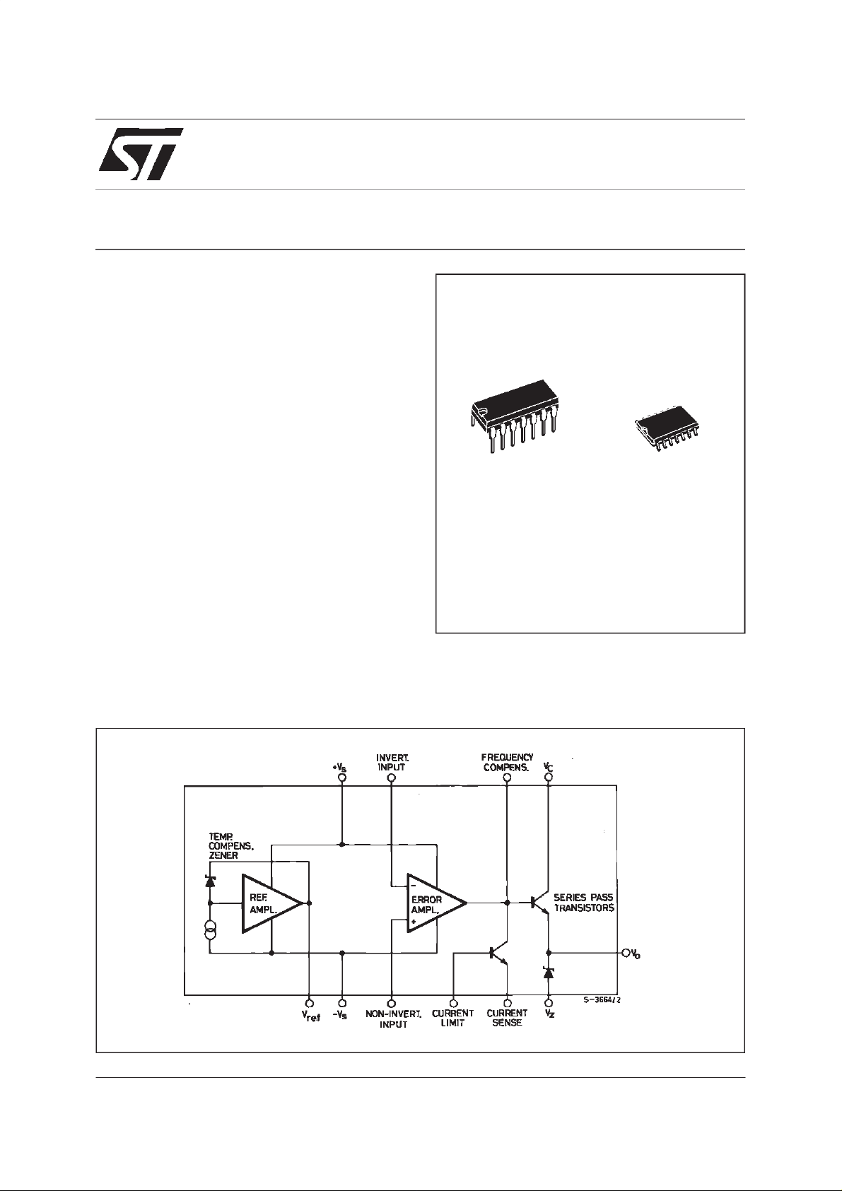
LM723
DESCRIPTION
The LM723 is a monolithic integrated
programmable voltage regulator, assembled in
14-lead dual in-line plastic and SO-14
micropackage. The circuit provides internal
current limiting. When the output current excedes
150mA an external NPN or PNP pass element
may be used.Provisions are made for adjustable
currentlimiting and remote shut-down.
BLOCK DIAGRAM
PlasticDIP-14 SO-14
September 1998
1/12
Page 2
LM723
ABSOLUTE MAXIMUM RATINGS
Symbol Parameter Value Unit
LM723 LM723C
DC InputVoltage 40 40 V
V
i
∆V
ABSOLUTE MAXIMUM RATINGS
Symbol Parameter Plastic DIP-14 SO-14 Unit
R
thj-amb
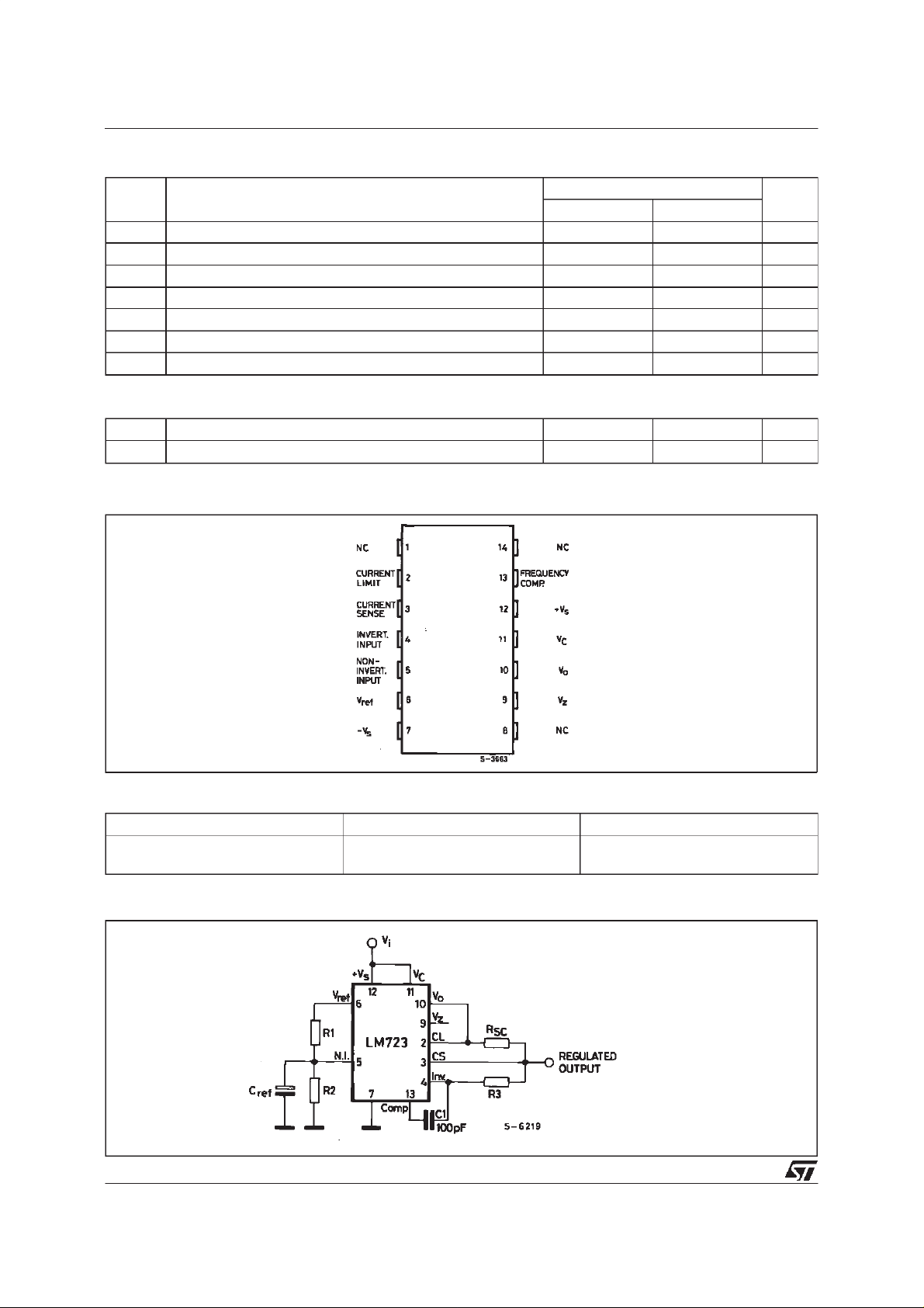
PINCONNECTION (top views)
Dropout Voltage 40 40 V
i-o
OutputCurrent 150 150 mA
I
o
Current fromV
I
ref
Operating Temperature -55 to 125 0 to 70
T
op
StorageTemperature -65 to 150 -65 to 150
T
stg
T
Junction Temperature 150 125
j
ref
15 25 mA
Thermal Resistance Junction-Ambient Max 200 160
o
o
C
o
C
o
C
C/W
ORDER CODES
Type Plastic DIP-14 SO-14
LM723
LM723C
LM723N
LM723CN LM723CD
TEST CIRCUIT (pin configurationrelativeto the plastic package)
2/12
Vi= 12V
V
=5V
o
I
= 1mA
o
R
1/R2
≤ 10KΩ
Page 3
LM723
ELECTRICAL CHARACTERISTICS FOR LM723 (refer to the testcircuits, T
amb
=25oC,
unless otherwisespecified)
Symbol Parameter Test Conditions Min. Typ. Max. Unit
/∆ViLineRegulation Vi=12 to 15V
∆V
o
∆V
V
LoadRegulation Io= 1 to50 mA
o/Vo
Reference Voltage
REF
SVR Supply Voltage Rejection f = 100Hz to10 KHz C
/∆T OutputVoltageDrift 150 ppm/oC
∆V
o
OutputCurrent Limit
I
sc
InputVoltageRange 9.5 40 V
V
i
OutputVoltage Range 2 37 V
V
o
V
o-Vi
Quiescent Current Vi=30V Io=0mA 2.35mA
I
d
LongTerm Stability 0.1 %/1000
K
VH
OutputNoiseVoltage BW = 100 Hz to10 KHz C
e
N
=12 to 40V
V
i
=12 to 15V -55oC ≤ T
V
i
= 1 to10 mA -55oC ≤ T
I
o
=160 µA
I
ref
ref
f = 100Hz to 10KHz C
=10Ω Vo=0
R
sc
ref
BW = 100Hz to 10 KHz C
amb
amb
=0
=5µF
ref
ref
≤ 125oC
≤ 125oC
6.95 7. 15 7.35 V
338V
=0
=5 µF
0.01
0.02
0.03 0. 15
74
86
65 mA
20
2.5
0.1
0.2
0.3
0.6
%
%
%
%
%
dB
dB
hrs
µV
µV
ELECTRICAL CHARACTERISTICS FOR LM723C (refer to the testcircuits, T
amb
=25oC,
unless otherwisespecified)
Symbol Parameter Test Conditions Min. Typ. Max. Unit
/∆ViLineRegulation Vi=12 to 15V
∆V
o
∆V
V
LoadRegulation Io= 1 to50 mA
o/Vo
Reference Voltage
REF
SVR Supply VoltageRejection f = 100Hz to 10KHz C
/∆T OutputVoltageDrift 150 ppm/oC
∆V
o
OutputCurrent Limit
I
sc
InputVoltageRange 9.5 40 V
V
i
OutputVoltage Range 2 37 V
V
o
V
o-Vi
Quiescent Current Vi=30V Io=0mA 2.34mA
I
d
LongTerm Stability 0.1 %/1000
K
VH
OutputNoiseVoltage BW = 100 Hz to10 KHz C
e
N
=12 to 40V
V
i
=12 to 15V 0oC ≤ T
V
i
= 1 to10 mA 0oC ≤ T
I
o
=160 µA
I
ref
f = 100Hz to 10KHz C
=10Ω Vo=0
R
sc
amb
amb
ref
ref
BW = 100Hz to 10 KHz C
≤ 70oC
≤ 70oC
=0
=5µF
=0
ref
=5 µF
ref
6.8 7.15 7.5 V
338V
0.01
0.1
0.03 0.2
74
86
65 mA
20
2.5
0.1
0.5
0.3
0.6
%
%
%
%
%
dB
dB
hrs
µV
µV
3/12
Page 4
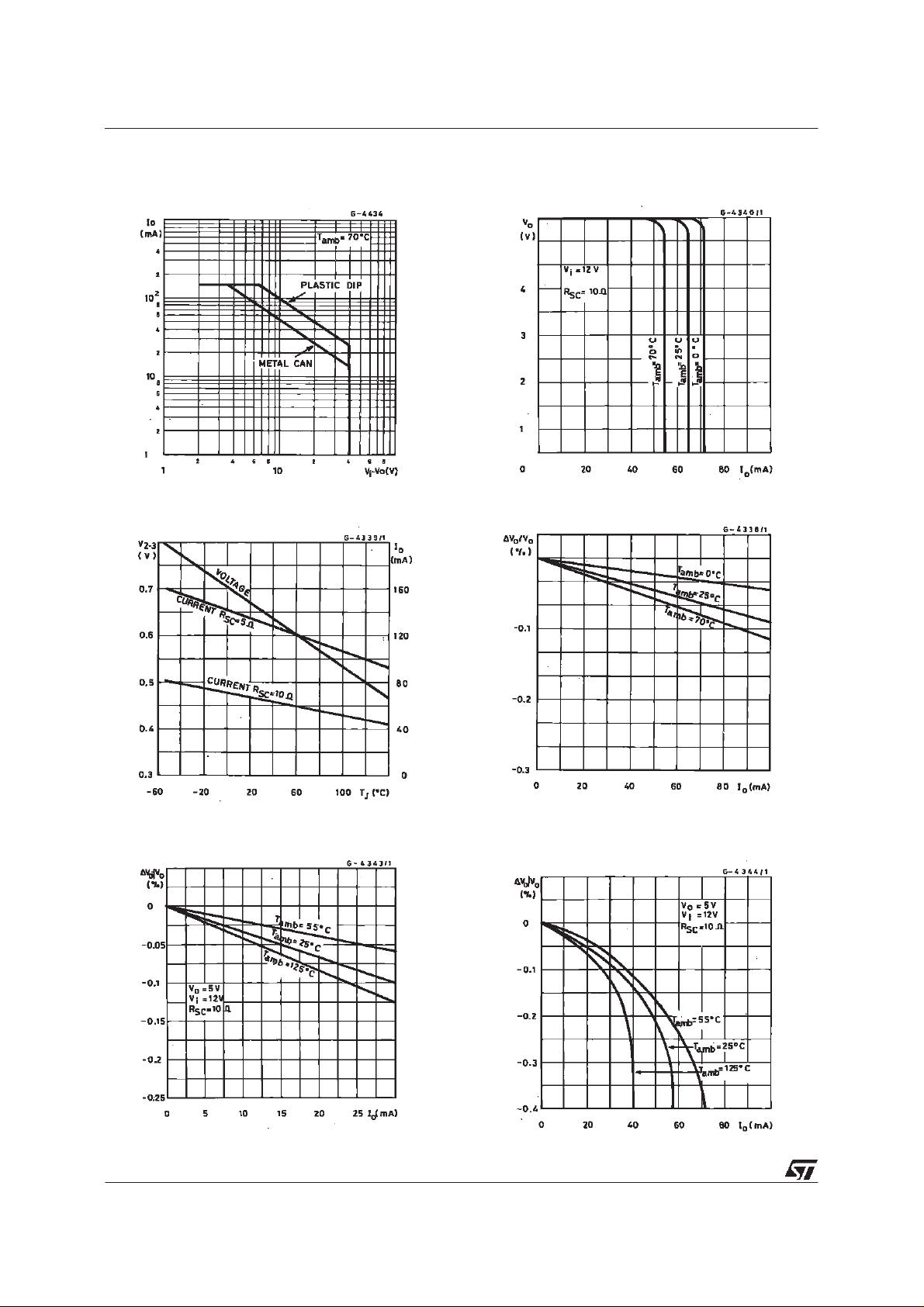
LM723
Figure1 : Maximum OutputCurrent vs. Voltage
Drop.
Figure3 : CurrentLimitingCharacteristicsvs.
JunctionTemperature.
Figure2 : CurrentLimiting Characteristics.
Figure4 : LoadRegulationCharacteristics
without CurrentLimiting.
Figure5 : LoadRegulationCharacteristicswith
CurrentLimiting.
4/12
Figure6 : LoadRegulationCharacteristicswith
Current Limiting
Page 5

LM723
Figure7 : LineRegulationvs. VoltageDrop. Figure 8 : Load Regulationvs.Voltage Drop.
Figure9 : QuiescentDrain Current vs. Input
Figure 10 : Line Transient Response.
Voltage.
Figure11 : Load TransientResponse. Figure 12 : OutputImpedancevs. Frequency.
5/12
Page 6

LM723
TABLE1: ResistorValues(KΩ) for standard Output Voltages
Output
Voltage
+3 1 3, 16, 1 7, 18 , 21 , 2 3 4.12 3.01 1.8 0.5 1. 2
+5 1 3, 16, 1 7, 18 , 21 , 2 3 2.15 4.99 0.75 0.5 2.2
+6 1 3, 16, 1 7, 18 , 21 , 2 3 1.15 6.04 0.5 0.5 2. 7
+9 1 4, 16, 1 7, 18 , 21 , 2 3 1.87 7.15 0.75 1 2.7
+12 14, 16, 17, 18, 21 , 2 3 4.87 7. 15 2 1 3
+15 14, 16, 17, 18, 21 , 2 3 7.87 7. 15 3.3 1 3
+28 14, 16, 17, 18, 21 , 2 3 21 7. 15 5.6 1 2
+45 19 3.57 4 8. 7 2.2 10 39
+75 19 3.57 7 8. 7 2.2 10 68
+100 19 3.57 102 2.2 10 91
+250 19 3.57 255 2.2 10 240
-6** 15 3.57 2 . 43 1.2 0. 5 0.7 5
-9 15 3.48 5.36 1.2 0.5 2
-12 15 3.57 8.45 1.2 0.5 3.3
-15 15 3.6 5 1 1. 5 1.2 0. 5 4. 3
-28 15 3.5 7 2 4. 3 1.2 0. 5 10
-45 20 3.5 7 2 1. 2 2.2 10 33
-100 20 3.57 97.6 2.2 10 91
-250 20 3.57 249 2.2 10 240
Note:
* Replace R1/R2 dividerwith the circuit of fig24.
** V+must beconnected to a +3V orgreater supply.
Applicable Figures Fixed Output± 5% Output Adjustable ± 10% *
R1 R2 R1 P1 R2
TABLE2: Formulaefor Intermediate Output Voltages
Outputsfrom+2to+7V
Fig. 13, 16, 17 , 18, 21, 23
=[V
V
O
ref
x
Out puts from +7 t o +37V
Fig.14, 16, 17, 1 8, 21, 23
V
=[V
ref
x
O
6/12
R
2
R1+ R
R
1+R2
R
2
]
2
]
Outpu t s from +4 to +250V
Fig. 19
R
V
ref
VO=
2
x
2
Outputsfrom-6to-250V
Fig. 15, 20
R
V
V
=
O
1
ref
x
2
− R
R
+ R
R
Current Limit ing
V
SENSE
=
I
1
;R
3=R4
1
LIMIT
R
sc
Foldbac k Current Limiting
OR3
=
x
4
V
V
SENSE(R3
SENSE
R
sc
V
=
KNEE
I
SHORT CKT
RscR
2
;R
3=R4
1
I
RscR
R
x
+ R
4
3+R4
R
4
4)
Page 7

APPLICATIONINFORMATION (pin numbers relative to the plasticpackage).
LM723
Figure13 : BasicLow VoltageRegulator
(V
= 2 to 7V).
o
R
×
R
1
Note; R3=
R3 may be eliminated for minimum component count.
Typical performance
RegulatedOutput Voltage....................................................5V
Line Regulation (∆V
Load Regulation (∆I
2
for minimum temperaturedrift.
R
+
R
1
2
= 3V).............................................0.5mV
i
=50mA)................... ................. ... 1.5mV
O
Figure 14 : BasicHigh VoltageRegulator
(Vo=7 to 37V).
R
×
R
1
2
Note; R
=
3
R3 may be eliminated for minimum component count.
Typical performance
Regulated Output Voltage..................................................15V
Line Regulation (∆V
Load Regulation (∆I
for minimum temperaturedrift.
R
+
R
1
2
= 3V).............. ................. ..............1.5mV
i
= 50mA)....................................... 4.5mV
O
Figure15 : Negative Voltage Regulator. Figure 16 : PositiveVoltageRegulator(external
Typical performance
Regulated Output Voltage.................... ............... ...............15V
Line Regulation (∆V
Load Regulation (∆I
= 3V)............................................... ..1mV
i
= 100mA)..................... ...................2mV
O
Typical performance
Regulated Output Voltage............... ................. ...............+15V
Line Regulation (∆V
Load Regulation (∆I
= 3V)........................ ................. ....1.5mV
i
= 1A).............................................15mV
O
7/12
Page 8

LM723
APPLICATIONINFORMATION (continued).
Figure17 : PositiveVoltage Regulator (External
Figure18 : Foldbackcurrent limiting
PNPPassTransistor)
Typical performance
RegulatedOutput Voltage....................................................5V
Line Regulation (∆V
Load Regulation (∆I
= 3V).............................................0.5mV
i
= 1 A) .................. .........................1.5mV
O
Typical performance
Regulated Output Voltage...................................................5 V
Line Regulation (∆V
Load Regulation (∆I
= 3V).............. ................. ..............0.5mV
i
= 10mA).......................................... 1mV
O
Current Limit Knee..................... ....................................20 mA
Figure19 : PositiveFloating Regulator Figure 20 : Negative FloatingRegulator
Typical performance
Regulated Output Voltage.................... ............... ............100 V
Line Regulation (∆V
Load Regulation (∆I
= 20V)........................................... 15 mV
i
= 50mA)....................... ............... 20 mV
O
8/12
Typical performance
Regulated Output Voltage............... ................. ............- 100 V
Line Regulation (∆V
Load Regulation (∆I
= 20V)...................... .....................30 mV
i
=100 mA)................................ .... 20 mV
O
Page 9

LM723
APPLICATIONINFORMATION (continued).
Figure21 : PositiveSwitchingRegulator Figure 22 : RemoteShutdown RegulatorWith
CurrentLimiting
Note: current limittransistor may be used for shutdown if
current limiting is notrequired.
Typical performance
RegulatedOutput Voltage...................................................5 V
Line Regulation (∆V
Load Regulation (∆I
= 30 V) ........................... ...............10mV
i
= 2 A) .................. .........................80 mV
O
Typical performance
Regulated Output Voltage...................................................5 V
Line Regulation (∆V
Load Regulation (∆I
= 3 V)...........................................0.5mV
i
= 50 mA)..................................... 1.5mV
O
Figure23 : ShuntRegulator. Figure 24 : OutputVoltageAdjust
Typical performance
Regulated Output Voltage.................... ............... ................5 V
Line Regulation (∆V
Load Regulation (∆I
= 10 V).............................................2 mV
i
= 100 mA)......................................5 mV
O
9/12
Page 10

LM723
Plastic DIP-14 MECHANICAL DATA
DIM.
MIN. TYP. MAX. MIN. TYP. MAX.
a1 0.51 0.020
B 1.39 1.65 0.055 0.065
b 0.5 0.020
b1 0.25 0.010
D 20 0.787
E 8.5 0.335
e 2.54 0.100
e3 15.24 0.600
F 7.1 0.280
I 5.1 0.201
L 3.3 0.130
Z 1.27 2.54 0.050 0.100
mm inch
10/12
P001A
Page 11

SO-14 MECHANICAL DATA
LM723
DIM.
MIN. TYP. MAX. MIN. TYP. MAX.
A 1.75 0.068
a1 0.1 0.2 0.003 0.007
a2 1.65 0.064
b 0.35 0.46 0.013 0.018
b1 0.19 0.25 0.007 0.010
C 0.5 0.019
c1 45 (typ.)
D 8.55 8.75 0.336 0.344
E 5.8 6.2 0.228 0.244
e 1.27 0.050
e3 7.62 0.300
F 3.8 4.0 0.149 0.157
G 4.6 5.3 0.181 0.208
L 0.5 1.27 0.019 0.050
M 0.68 0.026
S 8 (max.)
mm inch
P013G
11/12
Page 12

LM723
Information furnished is believed to beaccurate and reliable. However, STMicroelectronics assumes no responsibility for the consequences
of use of such information nor for any infringement of patents or other rights of third parties which may result from its use. No license is
granted by implication or otherwise under any patent or patent rights of STMicroelectronics. Specification mentioned in this publication are
subject to change without notice. This publication supersedes and replaces all information previously supplied. STMicroelectronics products
are not authorized for use as critical components inlife support devices or systems without express written approval ofSTMicroelectronics.
The ST logo is a trademark of STMicroelectronics
1998 STMicroelectronics –Printed in Italy – All RightsReserved
STMicroelectronics GROUP OF COMPANIES
Australia - Brazil -Canada -China -France - Germany- Italy - Japan - Korea - Malaysia - Malta - Mexico- Morocco- TheNetherlands -
12/12
Singapore - Spain - Sweden - Switzerland- Taiwan - Thailand- United Kingdom - U.S.A.
.
 Loading...