

Page 1
LM7131
Tiny High Speed Single Supply Operational Amplifier
General Description
The LM7131 is a high speed bipolar operational amplifier
available in a tiny SOT23-5 package. This makes the
LM7131 ideal for space and weight critical designs. Single
supply voltages of 3V and 5V provides good video performance, wide bandwidth, low distortion, and high PSRR and
CMRR. This makes the amplifier an excellent choice for
desktop and portable video and computing applications. The
amplifier is supplied in surface mount 8-pin and tiny
SOT23-5 packages.
Tiny amplifiers are so small they can be placed anywhere on
a board close to the signal source or next to an A-to-D input.
Good high speed performance at low voltage makes the
LM7131 a preferred part for battery powered designs.
Features
n Tiny SOT23-5 package saves space-typical circuit
layouts take half the space of SO-8 designs.
n Guaranteed specs at 3V, 5V, and
±
5V supplies
n Typical supply current 7.0 mA at 5V, 6.5 mA at 3V
n 4V output swing with +5V single supply
n Typical total harmonic distortion of 0.1%at 4 MHz
n 70 MHz Gain-Bandwidth Product
n 90 MHz −3 dB bandwidth at 3V and 5V, Gain=+1
n Designed to drive popular video A/D converters
n 40 mA output can drive 50Ω loads
n Differential gain and phase 0.25%and 0.75˚ at A
V
=
+2
Applications
n Driving video A/D converters
n Video output for portable computers and PDAs
n Desktop teleconferencing
n High fidelity digital audio
n Video cards
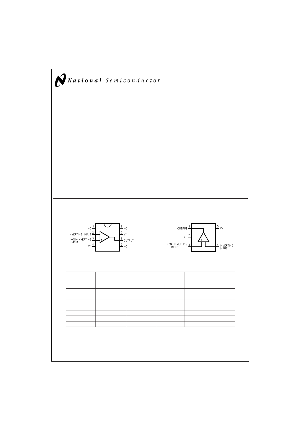
Connection Diagrams
Package Ordering NSC Drawing Package Supplied as
Information Number Marking
8-Pin SO-8 LM7131ACM M08A LM7131ACM rails
8-Pin SO-8 LM7131BCM M08A LM7131BCM rails
8-Pin SO-8 LM7131ACMX M08A LM7131ACM 2.5k units tape and reel
8-Pin SO-8 LM7131BCMX M08A LM7131BCM 2.5k units tape and reel
5-Pin SOT 23-5 LM7131ACM5 MA05A A02A 1k units on tape and reel
5-Pin SOT 23-5 LM7131BCM5 MA05A A02B 1k units on tape and reel
5-Pin SOT 23-5 LM7131ACM5X MA05A A02A 3k units tape and reel
5-Pin SOT 23-5 LM7131BCM5X MA05A A02B 3k units tape and reel
8-Pin SO-8
DS012313-1
Top View
5-Pin SOT23-5
DS012313-2
Top View
September 1999
LM7131 Tiny High Speed Single Supply Operational Amplifier
© 1999 National Semiconductor Corporation DS012313 www.national.com
Page 2
Absolute Maximum Ratings (Note 1)
If Military/Aerospace specified devices are required,
please contact the NationalSemiconductorSalesOffice/
Distributors for availability and specifications.
ESD Tolerance (Note 2) 2000V
Differential Input Voltage
±
2.0
Voltage at Input/Output Pin (V
+
)+0.1V, (V−) − 0.3V
Supply Voltage (V
+–V−
) 12V
Current at Input Pin
±
5mA
Current at Output Pin (Note 3)
±
80 mA
Current at Power Supply Pin
±
80 mA
Lead Temperature
(soldering, 10 sec) 260˚C
Storage Temperature Range − 65˚C to +150˚C
Junction Temperature (Note 4) 150˚C
Operating Ratings
Supply Voltage (V+–V−) 2.7V ≤ V ≤ 12V
Junction Temperature Range
LM7131AC, LM7131BC 0˚C ≤ T
J
≤ + 70˚C
Thermal Resistance (θ
JA
)
SO-8 Package, 8-Pin Surface Mount 165˚C/W
M05A Package, 5-Pin Surface Mount 325˚C/W
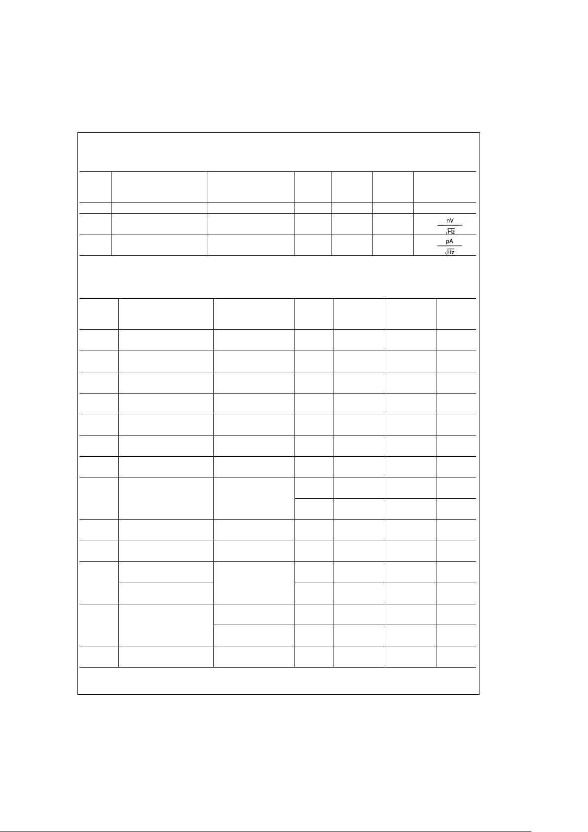
3V DC Electrical Characteristics
Unless otherwise specified, all limits guaranteed for T
J
=
25˚C, V
+
=
3V, V
−
=
0V, V
CM
=
V
O
=
V
+
/2 and R
L
=
150Ω. Bold-
face limits apply at the temperature extremes.
Symbol Parameter Conditions Typ
(Note 5)
LM7131AC LM7131BC Units
Limit Limit
(Note 6) (Note 6)
V
OS
Input Offset Voltage 0.02 3.5 7 mV
410max
TCV
OS
Input Offset Voltage 10 µV/˚C
Average Drift
I
B
Input Bias Current 20 35 35 µA
40 40 max
I
OS
Input Offset Current 0.35 3.5 3.5 µA
55max
CMRR Common Mode 0V ≤ V
CM
≤ 0.85V 75 60 60 dB
Rejection Ratio (Video Levels) 55 55 min
CMRR Common Mode 0.85V ≤ V
CM
≤ 1.7V 70 55 55 dB
Rejection Ratio (Mid-Range) 50 50 min
+PSRR Positive Power Supply V
+
=
3V, V
−
=
0V 75 65 65 dB
Rejection Ratio V
+
=
3V to 6.5V 60 60 min
−PSRR Negative Power Supply V
−
=
−3V, V
+
=
0V 75 65 65 dB
Rejection Ratio V
−
=
−3V to −6.5V 60 60 min
V
CM
Input Common-Mode V
+
=
3V 0.0 0.0 0.0 V
Voltage Range For CMRR ≥ 50 dB 0.00 0.00 min
2.0 1.70 1.70 V
1.60 1.60 max
A
VOL
Voltage Gain R
L
=
150Ω,V
O
=
0.250V 60 55 55 dB
to 1.250V 50 50
C
IN
Common-Mode 2 pF
Input Capacitance
V
O
Output Swing V
+
=
3V, R
L
=
150Ω 2.6 2.3 2.3 V
High terminated at 0V 2.0 2.0 min
Low V
+
=
3V, R
L
=
150Ω 0.05 0.15 0.15 V
terminated at 0V 0.20 0.20 max
High V
+
=
3V, R
L
=
150Ω 2.6 2.3 2.3 V
terminated at 1.5V 2.0 2.0 min
Low V
+
=
3V, R
L
=
150Ω 0.5 0.8 0.8 V
terminated at 1.5V 1.0 1.0 max
V
O
Output Swing V
+
=
3V, R
L
=
600Ω 2.73 V
High terminated at 0V max
www.national.com 2
Page 3
3V DC Electrical Characteristics (Continued)
Unless otherwise specified, all limits guaranteed for T
J
=
25˚C, V
+
=
3V, V
−
=
0V, V
CM
=
V
O
=
V
+
/2 and R
L
=
150Ω. Bold-
face limits apply at the temperature extremes.
Symbol Parameter Conditions Typ
(Note 5)
LM7131AC LM7131BC Units
Limit Limit
(Note 6) (Note 6)
V
O
Output Swing V
+
=
3V, R
L
=
600Ω 0.06 V
Low terminated at 0V max
I
SC
Output Short Circuit Sourcing, V
O
=
0V 65 45 45 mA
Current 40 40 min
Sinking, V
O
=
3V 40 25 25 mA
20 20 min
I
S
Supply Current V
+
=
+ 3V 6.5 9.0 9.0 mA
9.5 9.5 max
3V AC Electrical Characteristics
Unless otherwise specified, all limits guaranteed for T
J
=
25˚C, V
+
=
3V, V
−
=
0V, V
CM
=
V
O
=
V
+
/2 and R
L
=
150Ω. Bold-
face limits apply at the temperature extremes.
Symbol Parameter Conditions Typ
(Note 5)
LM7131AC LM7131BC Units
Limit Limit
(Note 6) (Note 6)
T.H.D. Total Harmonic Distortion F=4 MHz, A
V
=
+ 2 0.1
%
R
L
=
150Ω,V
O
=
1.0V
PP
Differential Gain (Note 10) 0.45
%
Differential Phase (Note 10) 0.6 ˚
SR Slew Rate R
L
=
150Ω,C
L
=
5 pF 120 V/µS
(Note 7)
SR Slew Rate R
L
=
150Ω,C
L
=
20 pF 100 V/µS
(Note 7)
GBW Gain-Bandwidth Product 70 MHz
Closed-Loop−3dB 90 MHz
Bandwidth
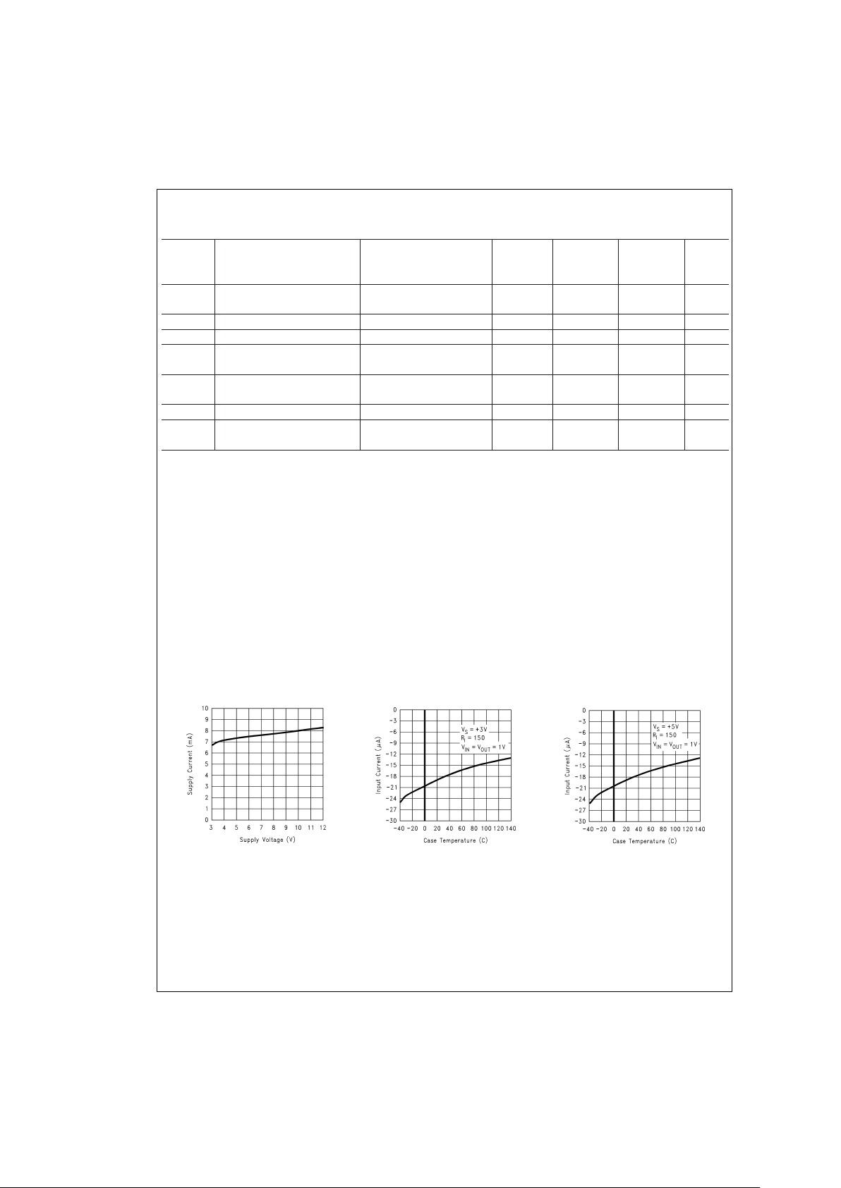
5V DC Electrical Characteristics
Unless otherwise specified, all limits guaranteed for T
J
=
25˚C, V
+
=
5V, V
−
=
0V, V
CM
=
V
O
=
V
+
/2 and R
L
=
150Ω. Bold-
face limits apply at the temperature extremes.
Symbol Parameter Conditions Typ
(Note 5)
LM7131AC LM7131BC Units
Limit Limit
(Note 6) (Note 6)
V
OS
Input Offset Voltage 0.02 3.5 7 mV
410max
TCV
OS
Input Offset Voltage 10 µV/˚C
Average Drift
I
B
Input Bias Current 20 35 35 µA
40 40 max
I
OS
Input Offset Current 0.35 3.5 3.5 µA
55max
CMRR Common Mode 0V ≤ V
CM
≤ 1.85V 75 65 65 dB
Rejection Ratio (Video Levels) 60 60 min
CMRR Common Mode 1.85V ≤ V
CM
≤ 3.7V 70 55 55 dB
Rejection Ratio (Mid-Range) 50 50 min
+ PSRR Positive Power Supply V
+
=
5V, V
−
=
0V 75 65 65 dB
www.national.com3
Page 4
5V DC Electrical Characteristics (Continued)
Unless otherwise specified, all limits guaranteed for T
J
=
25˚C, V
+
=
5V, V
−
=
0V, V
CM
=
V
O
=
V
+
/2 and R
L
=
150Ω. Bold-
face limits apply at the temperature extremes.
Symbol Parameter Conditions Typ
(Note 5)
LM7131AC LM7131BC Units
Limit Limit
(Note 6) (Note 6)
Rejection Ratio V
+
=
5V to 10V 60 60 min
− PSRR Negative Power Supply V
−
=
− 5V, V
+
=
0V 75 65 65 dB
Rejection Ratio V
−
=
− 5V to −10V 60 60 min
V
CM
Input Common-Mode V
+
=
5V 0.0 − 0.0 − 0.0 V
Voltage Range For CMRR ≥ 50 dB 0.00 0.00 min
4.0 3.70 3.70 V
3.60 3.60 max
A
VOL
Voltage Gain R
L
=
150Ω,V
O
=
70 60 60 dB
0.250V to 2.250V 55 55 min
C
IN
Common-Mode 2 pF
Input Capacitance
V
O
Output Swing V
+
=
5V, R
L
=
150Ω 4.5 4.3 4.3 V
High terminated at 0V 4.0 4.0 min
Low V
+
=
5V, R
L
=
150Ω 0.08 0.15 0.15 V
terminated at 0V 0.20 0.20 max
High V
+
=
5V, R
L
=
150Ω 4.5 4.3 4.3 V
terminated at 2.5V 4.0 4.0 min
Low V
+
=
5V, R
L
=
150Ω 0.5 0.8 0.8 V
terminated at 2.5V 1.0 1.0 max
V
O
Output Swing V
+
=
5V, R
L
=
600Ω 4.70 V
High terminated at 0V max
V
O
Ouptut Swing V
+
=
5V, R
L
=
600Ω 0.07 V
Low terminated at 0V max
I
SC
Output Short Circuit Sourcing, V
O
=
0V 65 45 45 mA
Current 40 40 min
Sinking, V
O
=
5V 40 25 25 mA
20 20 min
I
S
Supply Current V
+
=
+5V 7.0 9.5 9.5 mA
10.0 10.0 max
5V AC Electrical Characteristics
Unless otherwise specified, all limits guaranteed for T
J
=
25˚C, V
+
=
5V, V
−
=
0V, V
CM
=
V
O
=
V
+
/2 and R
L
=
150Ω. Bold-
face limits apply at the temperature extremes.
Symbol Parameter Conditions Typ
(Note 5)
LM7131AC LM7131BC Units
Limit Limit
(Note 6) (Note 6)
T.H.D. Total Harmonic Distortion F=4 MHz, A
V
=
+2 0.1
%
R
L
=
150Ω,V
O
=
2.0V
PP
Differential Gain (Note 10) 0.25
%
Differential Phase (Note 10) 0.75 ˚
SR Slew Rate R
L
=
150Ω,C
L
=
5 pF 150 V/µs
(Note 8)
SR Slew Rate R
L
=
150Ω,C
L
=
20 pF 130 V/µs
(Note 8)
GBW Gain-Bandwidth Product 70 MHz
Closed-Loop −3 dB 90 MHz
www.national.com 4
Page 5
5V AC Electrical Characteristics (Continued)
Unless otherwise specified, all limits guaranteed for T
J
=
25˚C, V
+
=
5V, V
−
=
0V, V
CM
=
V
O
=
V
+
/2 and R
L
=
150Ω. Bold-
face limits apply at the temperature extremes.
Symbol Parameter Conditions Typ
(Note 5)
LM7131AC LM7131BC Units
Limit Limit
(Note 6) (Note 6)
Bandwidth
e
n
Input-Referred f=1 kHz 11
Voltage Noise
i
n
Input-Referred f=1 kHz 3.3
Current Noise
±
5V DC Electrical Characteristics
Unless otherwise specified, all limits guaranteed for T
J
=
25˚C, V
+
=
5V, V
−
=
5V, V
CM
=
V
O
=
0V and R
L
=
150Ω. Boldface
limits apply at the temperature extremes.
Symbol Parameter Conditions Typ
(Note 5)
LM7131AC LM7131BC Units
Limit Limit
(Note 6) (Note 6)
V
OS
Input Offset Voltage 0.02 3.5 7 mV
410max
TCV
OS
Input Offset Voltage 10 µV/˚C
Average Drift
I
B
Input Bias Current 20 35 35 µA
40 40 max
I
OS
Input Offset Current 0.35 3.5 3.5 µA
55max
CMRR Common Mode −5V ≤ V
CM
≤ 3.7V 75 65 65 dB
Rejection Ratio 60 60 min
+PSRR Positive Power Supply V
+
=
5V, V
−
=
0V 75 65 65 dB
Rejection Ratio V
+
=
5V to 10V 60 60 min
−PSRR Negative Power Supply V
−
=
−5V, V
+
=
0V 75 65 65 dB
Rejection Ratio V
−
=
−5V to −10V 60 60 min
V
CM
Input Common-Mode V
+
=
5V, V
−
=
−5V −5.0 −5.0 −5.0 V
Voltage Range For CMRR ≥ 60 dB −5.0 −5.0 min
4.0 3.70 3.70 V
3.60 3.60 max
A
VOL
Voltage Gain R
L
=
150Ω,705555dB
V
O
=
−2.0 to +2.0 50 50
C
IN
Common-Mode 2 pF
Input Capacitance
V
O
Output Swing V
+
=
5V, V
−
=
−5V 4.5 4.3 4.3 V
High R
L
=
150Ω 4.0 4.0 min
Low terminated at 0V −4.5 −3.5 −3.5 V
−2.5 −2.5 max
I
SC
Output Short Circuit Sourcing, V
O
=
−5V 65 45 45 mA
Current 40 40 min
Sinking, V
O
=
5V 40 25 25 mA
20 20 min
I
S
Supply Current V
+
=
+5V, V
−
=
−5V 7.5 10.5 10.5 mA
11.5 11.5 max
www.national.com5
Page 6
±
5V AC Electrical Characteristics
Unless otherwise specified, all limits guaranteed for T
J
=
25˚C, V
+
=
5V, V
−
=
5V, V
CM
=
V
O
=
0V and R
L
=
150Ω. Boldface
limits apply at the temperature extremes.
Symbol Parameter Conditions Typ
(Note 5)
LM7131AC LM7131BC Units
Limit Limit
(Note 6) (Note 6)
T.H.D. Total Harmonic Distortion F=4 MHz, A
V
=
−2 1.5
%
R
L
=
150Ω,V
O
=
4.0V
PP
Differential Gain (Note 10) 0.25
%
Differential Phase (Note 10) 1.0 ˚
SR Slew Rate R
L
=
150Ω,C
L
=
5 pF 150 V/µs
(Note 9)
SR Slew Rate R
L
=
150Ω,C
L
=
20 pF 130 V/µs
(Note 9)
GBW Gain-Bandwidth Product 70 MHz
Closed-Loop −3 dB 90 MHz
Bandwidth
Note 1: Absolute maximum Ratings indicatelimits beyond which damage to the device may occur. Operating Ratings indicate conditions for which the device is intended to be functional, but specific performance is not guaranteed. For guaranteed specifications and the test conditions, see the Electrical characteristics.
Note 2: Human body model, 1.5 kΩ in series with 100 pF.
Note 3: Applies to both single-supply and split-supply operation. Continuous short circuit operation at elevated ambient temperature can result in exceeding the
maximum allowed junction temperature of 150˚C.
Note 4: The maximum power dissipation is a function of T
J(max)
, θJA, and TA. The maximum allowable power dissipation at any ambient temperature is P
D
=
(T
J(max)
-TA)/θJA. All numbers apply for packages soldered directly into a PC board.
Note 5: Typical values represent the most likely parametric norm.
Note 6: All limits are guaranteed by testing or statistical analysis.
Note 7: Connected as voltage follower with 1.5V step input. Number specified is the slower of the positive and negative slew rates. V
+
=
3V and R
L
=
150Ω con-
nected to 1.5V.Amp excited with 1 kHz to produce V
O
=
1.5 V
PP
.
Note 8: Connected as Voltage Follower with 4.0V step input. Number specified is the slower of the positive and negative slew rates. V
+
=
5V and R
L
=
150Ω con-
nected to 2.5V.Amp excited with 1 kHz to produce V
O
=
4V
PP
.
Note 9: Connected as Voltage Follower with 4.0V step input. Number specified is the slower of the positive and negative slew rates. V
+
=
5V, V
−
=
−5V and
R
L
=
150Ω connected to 0V.Amp excited with 1 kHz to produce V
O
=
4V
PP
.
Note 10: Differential gain and phase measured with a 4.5 MHz signal into a 150Ω load, Gain=+2.0, between 0.6V and 2.0V output.
Typical Performance Characteristics
LM7131 Supply Current vs
Supply Voltage
DS012313-27
LM7131 Input Current vs
Temperature
@
3V
DS012313-28
LM7131 Input Current vs
Temperature
@
5V
DS012313-29
www.national.com 6
Page 7
Typical Performance Characteristics (Continued)
LM7131 Input Current vs
Input Voltage
@
3V
DS012313-30
LM7131 Input Current vs
Input Voltage
@
5V
DS012313-31
LM7131 CMRR vs
Frequency
@
5V
DS012313-32
LM7131 Voltage Noise vs
Frequency
@
3V
DS012313-33
LM7131 Voltage Noise vs
Frequency
@
5V
DS012313-34
LM7131 PSRR vs
Frequency
@
3V
DS012313-35
LM7131 PSRR vs
Frequency
@
5V
DS012313-36
LM7131 Cable Driver
A
V
=
+1
@
+3V
DS012313-37
LM7131 Cable Driver
A
V
=
+2
@
+3V
DS012313-38
www.national.com7
Page 8

Typical Performance Characteristics (Continued)
LM7131 Driving 5'
RG-59 A
V
=
+2
@
+3V
DS012313-39
LM7131 Driving 75'
RG-59 A
V
=
+2
@
+3V
DS012313-40
LM7131 Cable Driver
A
V
=
+10
@
+3V
DS012313-41
LM7131 Cable Driver
A
V
=
+1
@
+5V
DS012313-42
LM7131 Cable Driver
A
V
=
+2
@
+5V
DS012313-43
LM7131 Driving 5' RG-59
A
V
=
+2
@
+5V
DS012313-44
LM7131 Driving 75' RG-59
A
V
=
+2
@
+5V
DS012313-45
LM7131 Cable Driver
A
V
=
+10
@
+5V
DS012313-46
LM7131 Driving Flash
A/D Load A
V
=
−1
@
+5V
DS012313-47
LM7131 Driving Flash
A/D Load A
V
=
+1
@
+5V
DS012313-48
LM7131 Driving Flash
A/D Load A
V
=
+2
@
+5V
DS012313-49
LM7131 Driving Flash
A/D Load A
V
=
+5
@
+5V
DS012313-50
www.national.com 8
Page 9

Typical Performance Characteristics (Continued)
Application Information
GENERAL INFORMATION
The LM7131 is a high speed complementary bipolar amplifier which provides high performance at single supply voltages. The LM7131 will operate at
±
5V split supplies, +5V
single supplies, and +3V single supplies. It can provide im-
proved performance for
±
5V designs with an easy transition
to +5V single supply.The LM7131 is a voltage feedback amplifier which can be used in most operational amplifier circuits.
LM7131 Driving Flash
A/D Load A
V
=
+5
@
+5V
With 2 pF Feedback Capacitor
DS012313-5
LM7131 Driving Flash
A/D Load A
V
=
+10
@
+5V
DS012313-6
LM7131 Bode Plot
@
3V, 5V and 10V
DS012313-7
LM7131 Single Supply
Bode Plot
@
3V, 5V and 10V
DS012313-8
www.national.com9
Page 10

Application Information (Continued)
The LM7131 is available in two package types: SO-8 surface
mount package and the SOT23-5 Tiny package for space
and weight savings.
The LM7131 has been designed to meet some of the most
demanding requirements for single supply
amplifiers— driving analog to digital converters and video
cable driving. The output stage of the LM7131 has been specially designed for the dynamic load presented by analog to
digital converters. The LM7131 is capable of a 4V output
range with a +5V single supply. The LM7131’s drive capability and good differential gain and phase make quality video
possible from a small package with only a +5V supply.
BENEFITS OF THE LM7131
The LM7131 can make it possible to amplify high speed signals with a single +5V or +3V supply, saving the cost of split
power supplies.
EASY DESIGN PATH FROM
±
5V to +5V SYSTEMS
The SO-8 package and similar
±
5V and single supply specifications means the LM7131 may be able to replace many
more expensive or slower op amps, and then be used for an
easy transition to 5V single supply systems. This could provide a migration path to lower voltages for the amplifiers in
system designs, reducing the effort and expense of testing
and re-qualifying different op amps for each new design.
In addition to providing a design migration path, the
SOT23-5 Tiny surface mount package can save valuable
board space.
SPECIFIC ADVANTAGES OF SOT23-5 (TINY PACKAGE)
The SOT23-5 (Tiny) package can save board space and allow tighter layouts. The low profile can help height limited designs, such as sub-notebook computers, consumer video
equipment, personal digital assistants, and some of the
thicker PCMCIA cards. The small size can improve signal integrity in noisy environments by placing the amplifier closer
to the signal source. The tiny amp can fit into tight spaces
and weighs little. This makes it possible to design the
LM7131 into places where amplifiers could not previously fit.
The LM7131 can be used to drive coils and transformers referenced to virtual ground, such as magnetic tape heads and
disk drive write heads. The small size of the SOT23-5 package can allow it to be placed with a pre-amp inside of some
rotating helical scan video head (VCR) assemblies. This
avoids long cable runs for low level video signals, and can
result in higher signal fidelity.
Additional space savings parts are available in tiny packages
from National Semiconductor, including low power amplifiers, precision voltage references, and voltage regulators.
Notes on Performance Curves and
Datasheet Limits
Important:
Performance curves represent an average of parts, and are
not limits.
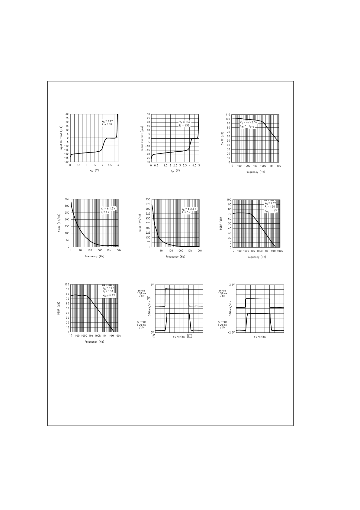
SUPPLY CURRENT vs SUPPLY VOLTAGE
Note that this curve is nearly straight, and rises slowly as the
supply voltage increases.
INPUT CURRENT vs INPUT VOLTAGE
This curve is relatively flat in the 200 mV to 4V input range,
where the LM7131 also has good common mode rejection.
COMMON MODE VOLTAGE REJECTION
Note that there are two parts to the CMRR specification of
the datasheet for 3V and 5V. The common mode rejection
ratio of the LM7131 has been maximized for signals near
ground (typical of the active part of video signals, such as
those which meet the RS-170 levels). This can help provide
rejection of unwanted noise pick-up by cables when a balanced input is used with good input resistor matching. The
mid-level CMRR is similar to that of other single supply op
amps.
BODE PLOTS (GAIN vs FREQUENCY FOR A
V
=
+1)
The gain vs. frequency plots for a non-inverting gain of 1
show the three voltages with the 150Ω load connected in two
ways. For the single supply graphs, the load is connected to
the most negative rail, which is ground. For the split supply
graphs, the load is connected to a voltage halfway between
the two supply rails.
DRIVING CABLES
Pulse response curves for driving 75Ω back terminate cables
are shown for both 3V and 5V supplies. Note the good pulse
fidelity with straight 150 loads, five foot (1.5 meter) and 75
foot (22 meter) cable runs. The bandwidth is reduced when
used in a gain of ten (A
V
=
+10). Even in a gain of ten con-
figuration, the output settles to
<
1%in about 100 ns, making this useful for amplifying small signals at a sensor or signal source and driving a cable to the main electronics section
which may be located away from the signal source. This will
reduce noise pickup.
Please refer to
Figures 1, 2, 3, 4, 5
for schematics of test set-
ups for cable driving.
www.national.com 10
Page 11

Notes on Performance Curves and Datasheet Limits (Continued)
DS012313-9
Numbers in parentheses are measured
fixture capacitances w/o DUT and load.
FIGURE 1. Cable Driver A
V
=
+1
DS012313-10
Numbers in parentheses are measured
fixture capacitances w/o DUT and load.
FIGURE 2. Cable Driver A
V
=
+2
DS012313-11
Numbers in parentheses are measured
fixture capacitances w/o DUT and load.
FIGURE 3. Cable Driver 5' RG-59
www.national.com11
Page 12

Notes on Performance Curves and Datasheet Limits (Continued)
DRIVING TYPE 1175 FLASH A/D LOADS
The circuits in
Figures 6, 7, 8, 9, 10, 11
show a LM7131 in a
voltage follower configuration driving the passive equivalent
of a typical flash A/D input. Note that there is a slight ringing
on the output, which can affect accurate analog-to-digital
conversion. In these graphs, we have adjusted the ringing to
be a little larger than desirable in order to better show the
settling time. Most settling times at low gain are about 75 ns
to
<
1%of final voltage. The ringing can be reduced by adding a low value (approximately 500Ω) feedback resistor from
the output to the inverting input and placing a small (pico-
farad range) capacitor across the feedback resistor. See
Fig-
ure 9
and
Figure 10
for schematics and respective perfor-
mance curves for flash A/D driving at A
V
=
+5 with and
withouta2pFfeedback capacitor.
See section on feedback compensation. Ringing can also be
reduced by placing an isolation resistor between the output
and the analog-to-digital converter input— see sections on
driving capacitive loads and analog-to-digital converters.
Please refer to
Figures 6, 7, 8, 9, 10, 11
for schematics of
test setups for driving flash A/D converters.
DS012313-12
Numbers in parentheses are measured
fixture capacitances w/o DUT and load.
FIGURE 4. Cable Driver 75' RG-59
DS012313-13
Numbers in parentheses are measured
fixture capacitances w/o DUT and load.
FIGURE 5. Cable Driver Gain of 10 A
V
=
+10
www.national.com 12
Page 13

Notes on Performance Curves and Datasheet Limits (Continued)
DS012313-14
Numbers in parentheses are measured
fixture capacitances w/o DUT and load.
FIGURE 6. Flash A/D A
V
=
−1
DS012313-15
Numbers in parentheses are measured
fixture capacitances w/o DUT and load.
FIGURE 7. Flash A/D A
V
=
+1
www.national.com13
Page 14

Notes on Performance Curves and Datasheet Limits (Continued)
DS012313-16
Numbers in parentheses are measured
fixture capacitances w/o DUT and load.
FIGURE 8. Flash A/D A
V
=
+2
DS012313-17
Numbers in parentheses are measured
fixture capacitances w/o DUT and load.
FIGURE 9. Flash A/D A
V
=
+5
www.national.com 14
Page 15

Notes on Performance Curves and Datasheet Limits (Continued)
Using the LM7131
LIMITS AND PRECAUTIONS
Supply Voltage
The absolute maximum supply voltage which may be applied to the LM7131 is 12V. Designers should not design for
more than 10V nominal, and carefully check supply tolerances under all conditions so that the voltages do not exceed the maximum.
Differential Input Voltage
Differential input voltage is the difference in voltage between
the non-inverting (+) input and the inverting input (−) of the
op amp. The absolute maximum differential input voltage is
±
2V across the inputs. This limit also applies when there is
no power supplied to the op amp. This may not be a problem
in most conventional op amp designs, however, designers
should avoid using the LM7131 as comparator or forcing the
inputs to different voltages. In some designs, diode protection may be needed between the inputs. See
Figure 12
.
DS012313-18
Numbers in parentheses are measured
fixture capacitances w/o DUT and load.
FIGURE 10. Flash A/D A
V
=
+5 with Feedback Capacitor
DS012313-19
Numbers in parentheses are measured
fixture capacitances w/o DUT and load.
FIGURE 11. Flash A/D A
V
=
+10
www.national.com15
Page 16

Using the LM7131 (Continued)
Output Short Circuits
The LM7131 has output short circuit protection, however, it is
not designed to withstand continuous short circuits, very fast
high energy transient voltage or current spikes, or shorts to
any voltage beyond the power supply rails. Designs should
reduce the number and energy level of any possible output
shorts, especially when used with
±
5V supplies.
A resistor in series with the output, such as the 75Ω resistor
used to back terminate 75Ω cables, will reduce the effects of
shorts. For outputs which will send signals off the PC board
additional protection devices, such as diodes to the power
rails, zener-type surge suppressors, and varistors may be
useful.
Thermal Management
Note that the SOT23-5 (Tiny) package has less power dissipation capability (325˚/W) than the S0-8 package (115˚/W).
This may cause overheating with
±
5 supplies and heavy
loads at high ambient temps. This is less of a problem when
using +5V single supplies.
Example:
Driving a 150Ω load to 2.0V at a 40˚C (104 ˚F) ambient tem-
perature. (This is common external maximum temperature
for office environments. Temperaturesinside equipment may
be higher.)
No load powerNo load LM7131 supply current - 9.0 mA
Supply voltage is 5.0V
No load LM7131 power - 9.0 mA x 5.0V=45 mW
Power with loadCurrent out is 2.0V/150 Ω=13.33 mA
Voltage drop in LM7131 is 5.0V (supply) − 2.0V (output)
=
3.0V
Power dissipation 13.33 mA x 3.0V=40 mW
Total Power=45mW+40mW=85 mW=0.085
Temperature Rise=0.085 W x 325˚/W=27.625 degrees
Junction temperature at 40˚ ambient=40 + 27.625
=
67.6225˚.
This device is within the 0˚ to 70˚ specification limits.
The 325˚/W value is based on still air and the pc board land
pattern shown in this datasheet. Actual power dissipation is
sensitive to PC board connections and airflow.
SOT23-5 power dissipation may be increased by airflow or
by increasing the metal connected to the pads, especially
the center pin (pin number 2, V−) on the left side of the
SOT23-5. This pin forms the mounting paddle for the die inside the SOT23-5, and can be used to conduct heat away
from the die. The land pad for pin 2 can be made larger
and/or connected to power planes in a multilayer board.
Additionally, it should be noted that difficulty in meeting performance specifications for the LM7131 is most common at
cold temperatures. While excessively high junction temperatures will degrade LM7131 performance, testing has confirmed that most specifications are met at a junction temperature of 85˚C.
See “Understanding Integrated Circuit Package Power Capabilities”, Application Note AN-336, which may be found in
the appendix of the Operational Amplifier Databook.
Layout and Power Supply Bypassing
Since the LM7131 is a high speed (over 50 MHz) device,
good high speed circuit layout practices should be followed.
This should include the use of ground planes, adequate
power supply bypassing, removing metal from around the input pins to reduce capacitance, and careful routing of the
output signal lines to keep them away from the input pins.
The power supply pins should be bypassed on both the
negative and positive supply inputs with capacitors placed
close to the pins. Surface mount capacitors should be used
for best performance, and should be placed as close to the
pins as possible. It is generally advisable to use two capacitors at each supply voltage pin. A small surface mount capacitor with a value of around 0.01 microfarad (10 nF), usually a ceramic type with good RF performance, should be
placed closest to the pin. A larger capacitor, in usually in the
range of 1.0 µF to 4.7 µF,should also be placed near the pin.
The larger capacitor should be a device with good RF characteristics and low ESR (equivalent series resistance) for
best results. Ceramic and tantalum capacitors generally
work well as the larger capacitor.
For single supply operation, if continuous low impedance
ground planes are available, it may be possible to use bypass capacitors between the +5V supply and ground only,
and reduce or eliminate the bypass capacitors on the V− pin.
Capacitive Load Driving
The phase margin of the LM7131 is reduced by driving large
capacitive loads. This can result in ringing and slower settling of pulse signals. This ringing can be reduced by placing
a small value resistor (typically in the range of 22Ω–100Ω)
between the LM7131 output and the load. This resistor
should be placed as close as practical to the LM7131 output.
When driving cables, a resistor with the same value as the
characteristic impedance of the cable may be used to isolate
the cable capacitance from the output. This resistor will reduce reflections on the cable.
Input Current
The LM7131 has typical input bias currents in the 15 µA to
25 µA range. This will not present a problem with the low input impedances frequently used in high frequency and video
circuits. For a typical 75Ω input termination, 20 µA of input
current will produce a voltage across the termination resistor
of only 1.5 mV. An input impedance of 10 kΩ, however,
would produce a voltage of 200 mV, which may be large
compared to the signal of interest. Using lower input impedances is recommended to reduce this error source.
Gain of +2
DS012313-20
FIGURE 12.
www.national.com 16
Page 17

Using the LM7131 (Continued)
Feedback Resistor Values and Feedback
Compensation
Using large values of feedback resistances (roughly 2k) with
low gains (such gains of 2) will result in degraded pulse response and ringing. The large resistance will form a pole
with the input capacitance of the inverting input, delaying
feedback to the amplifier. This will produce overshoot and
ringing. To avoid this, the gain setting resistors should be
scaled to lower values (below 1k)At higher gains (
>
5) larger
values of feedback resistors can be used.
Overshoot and ringing of the LM7131 can be reduced by
adding a small compensation capacitor across the feed back
resistor.For the LM7131 values in pF to tens of pF range are
useful initial values. Too large a value will reduce the circuit
bandwidth and degrade pulse response.
Since the small stray capacitance from the circuit layout,
other components, and specific circuit bandwidth requirements will vary, it is often useful to select final values based
on prototypes which are similar in layout to the production
circuit boards.
Reflections
The output slew rate of the LM7131 is fast enough to produce reflected signals in many cables and long circuit traces.
For best pulse performance, it may be necessary to terminate cables and long circuit traces with their characteristic
impedance to reduce reflected signals.
Reflections should not be confused with overshoot. Reflections will depend on cable length, while overshoot will depend on load and feedback resistance and capacitance.
When determining the type of problem, often removing or
drastically shortening the cable will reduce or eliminate reflections. Overshoot can exist without a cable attached to the
op amp output.
Driving Flash A/D Converters (Video Converters)
The LM7131 has been optimized to drive flash analog to
digital converters in a +5V only system. Different flash A/D
converters have different voltage input ranges. The LM7131
has enough gain-bandwidth product to amplify standard
video level signals to voltages which match the optimum input range of many types of A/D converters.
For example, the popular 1175 type 8-bit flash A/D converter
has a preferred input range from 0.6V to 2.6V. If the input
signal has an active video range (excluding sync levels) of
approximately 700 mV,a circuit like the one in
Figure 13
can
be used to amplify and drive an A/D. The 10 µF capacitor
blocks the DC components, and allows the + input of the
LM7131 to be biased through R clamp so that the minimum
output is equal to V
RB
of the A/D converter. The gain of the
circuit is determined as follows:
Output Signal Range=2.6V (V top)=0.6V (V bottom)
=
2.0V
Gain=Output Signal Range/Input Signal=2.857
=
2.00/0.700
Gain=(R
f/R1
)+1=(249Ω/133Ω)+1
R isolation and C
f
will be determined by the designer
based on the A/D input capacitance and the desired pulse
response of the system. The nominal values of 33Ω and 5.6
pF shown in the schematic may be a useful starting point,
however, signal levels, A/D converters, and system performance requirements will require modification of these values.
The isolation resistor, R isolation should be placed close to
the output of the LM7131, which should be close to the A/D
input for best results.
R clamp is connected to a voltage level which will result in
the bottom of the video signal matching the Vrb level of the
A/D converter. This level will need to be set by clamping the
black level of the video signal. The clamp voltage will depend
on the level and polarity of the video signal. Detecting the
sync signal can be done by a circuit such as the LM1881
Video Sync Separator.
Note: This is an illustration of a conceptual use of the LM7131, not a com-
plete design. The circuit designer will need to modify this for input protection, sync, and possibly some type of gain control for varying signal
levels.
Some A/D converters have wide input ranges where the
lower reference level can be adjusted. With these converters, best distortion results are obtained if the lower end of the
output range is about 250 mV or more above the V− input of
the LM7131 more. The upper limit can be as high as 4.0V
with good results.
www.national.com17
Page 18

Using the LM7131 (Continued)
CCD Amplifiers
The LM7131 has enough gain bandwidth to amplify low level
signals from a CCD or similar image sensor and drive a flash
analog-to-digital converter with one amplifier stage.
Signals from CCDs, which are used in scanners, copiers,
and digital cameras, often have an output signal in the 100
mV–300 mV range. See
Figure 14
for a conceptual diagram.
With a gain of 6 the output to the flash analog-to- digital converter is 1.8V, matching 90%of the converter’s 2V input
range. With a −3db bandwidth of 70 MHz for a gain of +1, the
bandwidth at a gain of 6 will be 11.6 MHz. This 11.6 MHz
bandwidth will result in a time constant of about 13.6 ns. This
will allow the output to settle to 7 bits of accuracy within 4.9
time constants, or about 66 ns. Slewing time for a 1.8V step
will be about 12 ns. The total slewing and settling time will be
about 78 ns of the 150 ns pixel valid time. This will leave
about 72 ns total for the flash converter signal acquisition
time and tolerance for timing signals.
For scanners and copiers with moving scan bars, the
SOT23-5 package is small enough to be placed next to the
light sensor.The LM7131 can drive a cable to the main electronics section from the scan bar. This can reduce noise
pickup by amplifying the signal before sending on the cable.
A/D Reference Drivers
The LM7131’s output and drive capability make it a good
choice for driving analog-to-digital references which have
suddenly changing loads. The small size of the SOT23-5
package allow the LM7131 to be placed very close to the A/D
reference pin, maximizing response. The small size avoids
the penalty of increased board space. Often the SOT23-5
package is small enough that it can fit in space used by the
large capacitors previously attached to the A/D reference. By
acting as a buffer for a reference voltage, noise pickup can
be reduced and the accuracy may be increased.
For additional space savings, the LM4040 precision voltage
reference and LM385 low current voltage reference are
available in a tiny SOT23-3 package.
Video Gain of +2
The design of the LM7131 has been optimized for gain of +2
video applications. Typical values for differential gain and
phase are 0.25%differential gain and 0.75 degree differential phase. See
Figure 12
.
Improving Video Performance
Differential gain and phase performance can be improved by
keeping the active video portion of the signal above 300 mV.
The sync signal can go below 300 mV without affecting the
video quality.If it is possible toAC couple the signal and shift
the output voltage slightly higher, much better video performance is possible. For a +5V single supply, an output range
between 2.0V and 3.0V can have a differential gain of 0.07
%
and differential phase of 0.3 degree when driving a 150Ω
load. For a +3V single supply,the output should be between
1.0V and 2.0V.
Cable Driving with +5V Supplies
The LM7131 can easily drive a back-terminated 75Ω video
cable (150Ω load) when powered by a +5V supply. See
Fig-
ures 2, 3, 4
. This makes it a good choice for video output for
portable equipment, personal digital devices, and desktop
video applications.
DS012313-21
FIGURE 13.
www.national.com 18
Page 19

Using the LM7131 (Continued)
The LM7131 can also supply +2.00V to a 50Ω load to
ground, making it useful as driver in 50Ω systems such as
portable test equipment.
Cable Driving with +3V Supplies
The LM7131 can drive 150Ω to 2.00V when supplied by a 3V
supply.This 3V performance means that the LM7131 is use-
ful in battery powered video applications, such as camcorders, portable video mixers, still video cameras, and portable
scanners.
Audio and High Frequency Signal Processing
The LM7131 is useful for high fidelity audio and signal processing. A typical LM7131 is capable of driving 2V across
150Ω (referenced to ground) at less than 0.1%distortion at
4 MHz when powered by a single 5V supply.
Use with 2.5V Virtual Ground Systems
with +5V Single Supply Power
Many analog systems which must work on a single +5V supply use a “virtual ground” - a reference voltage for the signal
processing which is usually between +5V and 0V.This virtual
ground is usually halfway between the top and bottom supply rails. This is usually +2.5V for +5V systems and +1.5V for
+3V systems.
The LM7131 can be used in single supply/virtual ground systems driving loads referenced to 2.5V. The output swing
specifications in the data sheet show the tested voltage limits for driving a 150Ω load to a virtual ground supply for +3V
and +5V.A look at the output swing specifications shows that
for heavy loads like 150 ohms, the output will swing as close
as one diode drop (roughly, 0.7V) to the supply rail. This
leaves a relatively wide range for +5V systems and a somewhat narrow range for +3V systems. One way to increase
this output range is to have the output load referenced to
ground— this will allow the output to swing lower.Another is
to use higher load impedances. The output swing specifications show typical numbers for swing with loads of 600Ω to
ground. Note that these typical numbers are similar to those
for a 150Ω load. These typical numbers are an indication of
the maximum DC performance of the LM7131.
The sinking output of the LM7131 is somewhat lower than
the amplifier’s sourcing capability. This means that the
LM7131 will not drive as much current into a load tied to 2.5
V as it will drive into a load tied to 0V.
Good AC performance will require keeping the output further
away from the supply rails. For a +5V supply and relatively
high impedance load (analog-to-digital converter input) the
following are suggested as an initial starting range for
achieving high (
>
60 dB) AC accuracy
Upper output level—
Approximately 0.8V to 1V below the positive (V+) rail.
Lower output level—
Approximately 200 mV–300 mV above the negative rail.
The LM7131 very useful in virtual ground systems as an out-
put device for output loads which are referenced to 0V or the
lower rail. It is also useful as a driver for capacitive loads,
such as sample and hold circuits, and audio analog to digital
converters. If fast amplifiers with rail-to-rail output ranges are
needed, please see the National Semiconductor LM6142
datasheet.
DS012313-23
FIGURE 14. CCD Amplifier
www.national.com19
Page 20

Using the LM7131 (Continued)
D/A Output Amplifier
The LM7131 can be used as an output amplifier for fast
digital-to-analog converters. When using the LM7131 with
converters with an output voltage range which may exceed
the differential input voltage limit of
±
2V,it may be necessary
to add protection diodes to the inputs. See
Figure 15
. For
high speed applications, it may be useful to consider low capacitance schottky diodes. Additional feedback capacitance
may be needed to control ringing due to the additional input
capacitance from the D/A and protection diodes. When used
with current output D/As, the input bias currents may produce a DC offset in the output. This offset may be canceled
by a resistor between the positive input and ground.
Spice Macromodel
A SPICE macromodel of the LM7131 and many other National Semiconductor op amps is available at no charge from
your National Semiconductor representative.
DS012313-24
FIGURE 15. D/A Ouput Amplifier
www.national.com 20
Page 21

SOT-23-5 Tape and Reel Specification
TAPE FORMAT
Tape Section
#
Cavaties Cavity Status Cover Tape Status
Leader 0 (min) Empty Sealed
(Start End) 75 (min) Empty Sealed
Carrier 3000 Filled Sealed
1000 Filled Sealed
Trailer 125 (min) Empty Sealed
(Hub End) 0 (min) Empty Sealed
TAPE DIMENSIONS
8 mm 0.130 0.124 0.130 0.126 0.138±0.002 0.055±0.004 0.157 0.315±0.012
(3.3) (3.15) (3.3) (3.2) (3.5
±
0.05) (1.4±0.11) (4) (8±0.3)
Tape Size DIM A DIM Ao DIM B DIM Bo DIM F DIM Ko DIM P1 DIM W
DS012313-25
www.national.com21
Page 22

SOT-23-5 Tape and Reel Specification (Continued)
REEL DIMENSIONS
8 mm 7.00 0.059 0.512 0.795 2.165 0.331 +0.059/−0.000 0.567 W1 + 0.078/−0.039
330.00 1.50 13.00 20.20 55.00 8.4 + 1.50/−0.00 14.40 W1 + 2.00/−1.00
Tape Size A B C D N W1 W2 W3
DS012313-26
www.national.com 22
Page 23

Physical Dimensions inches (millimeters) unless otherwise noted
LIFE SUPPORT POLICY
NATIONAL’S PRODUCTS ARE NOT AUTHORIZED FOR USE AS CRITICAL COMPONENTS IN LIFE SUPPORT
DEVICES OR SYSTEMS WITHOUT THE EXPRESS WRITTEN APPROVAL OF THE PRESIDENT AND GENERAL
COUNSEL OF NATIONAL SEMICONDUCTOR CORPORATION. As used herein:
1. Life support devices or systems are devices or
systems which, (a) are intended for surgical implant
into the body, or (b) support or sustain life, and
whose failure to perform when properly used in
accordance with instructions for use provided in the
labeling, can be reasonably expected to result in a
significant injury to the user.
2. A critical component is any component of a life
support device or system whose failure to perform
can be reasonably expected to cause the failure of
the life support device or system, or to affect its
safety or effectiveness.
National Semiconductor
Corporation
Americas
Tel: 1-800-272-9959
Fax: 1-800-737-7018
Email: support@nsc.com
National Semiconductor
Europe
Fax: +49 (0) 1 80-530 85 86
Email: europe.support@nsc.com
Deutsch Tel: +49 (0) 1 80-530 85 85
English Tel: +49 (0) 1 80-532 78 32
Français Tel: +49 (0) 1 80-532 93 58
Italiano Tel: +49 (0) 1 80-534 16 80
National Semiconductor
Asia Pacific Customer
Response Group
Tel: 65-2544466
Fax: 65-2504466
Email: sea.support@nsc.com
National Semiconductor
Japan Ltd.
Tel: 81-3-5639-7560
Fax: 81-3-5639-7507
www.national.com
5-Pin SOT Package
Order Package Number LM7131ACM5, LM7131ACM5X, LM7131BCM5 or LM7131BCM5X
NS Package Number MA05A
LM7131 Tiny High Speed Single Supply Operational Amplifier
National does not assume any responsibility for use of any circuitry described, no circuit patent licenses are implied and National reserves the right at any time without notice to change said circuitry and specifications.
 Loading...