

Page 1
TL/H/11477
LM709 Operational Amplifier
February 1995
LM709
Operational Amplifier
General Description
The LM709 series is a monolithic operational amplifier intended for general-purpose applications. Operation is completely specified over the range of voltages commonly used
for these devices. The design, in addition to providing high
gain, minimizes both offset voltage and bias currents. Further, the class-B output stage gives a large output capability
with minimum power drain.
External components are used to frequency compensate
the amplifier. Although the unity-gain compensation network
specified will make the amplifier unconditionally stable in all
feedback configurations, compensation can be tailored to
optimize high-frequency performance for any gain setting.
The LM709C is the commercial-industrial version of the
LM709. It is identical to the LM709 except that it is specified
for operation from 0
§
Ctoa70§C.
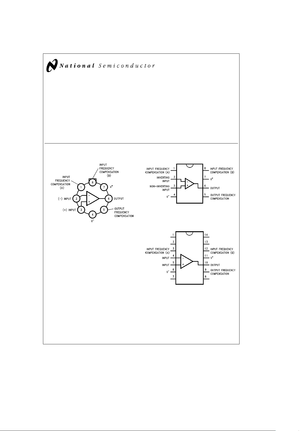
Connection Diagrams
Metal Can Package
TL/H/11477– 4
Order Number LM709AH, LM709H or LM709CH
See NS Package Number H08C
Dual-In-Line Package
TL/H/11477– 6
Order Number LM709CN-8
See NS Package Number N08E
Dual-In-Line Package
TL/H/11477– 5
Order Number LM709CN
See NS Package Number N14A
C
1995 National Semiconductor Corporation RRD-B30M115/Printed in U. S. A.
Page 2
Absolute Maximum Ratings (Note 3)
If Military/Aerospace specified devices are required,
please contact the National Semiconductor Sales
Office/Distributors for availability and specifications.
Supply Voltage
LM709/LM709A/LM709C
g
18V
Power Dissipation (Note 1)
LM709/LM709A 300 mW
LM709C 250 mW
Differential Input Voltage
LM709/LM709A/LM709C
g
5V
Input Voltage
LM709/LM709A/LM709C
g
10V
Output Short-Circuit Duration (T
A
ea
25§C)
LM709/LM709A/LM709C 5 seconds
Storage Temperature Range
LM709/LM709A/LM709C
b
65§Ctoa150§C
Lead Temperature (Soldering, 10 sec.)
LM709/LM709A/LM709C 300
§
C
Operating Ratings (Note 3)
Junction Temperature Range (Note 1)
LM709/LM709A
b
55§Ctoa150§C
LM709C 0
§
Ctoa100§C
Thermal Resistance (iJA)
H Package 150
§
C/W, (iJC)45§C/W
8-Pin N Package 134
§
C/W
14-Pin N Package 109
§
C/W
Electrical Characteristics (Note 2)
Parameter Conditions
LM709A LM709 LM709C
Units
Min Typ Max Min Typ Max Min Typ Max
Input Offset Voltage T
A
e
25§C, R
S
s
10 kX 0.6 2.0 1.0 5.0 2.0 7.5 mV
Input Bias Current T
A
e
25§C 100 200 200 500 300 1500 nA
Input Offset Current T
A
e
25§C 10 50 50 200 100 500 nA
Input Resistance T
A
e
25§C 350 700 150 400 50 250 kX
Output Resistance T
A
e
25§C 150 150 150 X
Supply Current T
A
e
25§C, V
S
e
g
15V 2.5 3.6 2.6 5.5 2.6 6.6 mA
Transient Response V
IN
e
20 mV, C
L
s
100 pF
Risetime T
A
e
25§C 1.5 0.3 1.0 0.3 1.0 ms
Overshoot 30 10 30 10 30 %
Slew Rate T
A
e
25§C 0.25 0.25 0.25 V/ms
Input Offset Voltage R
S
s
10 kX 3.0 6.0 10 mV
Average Temperature R
S
e
50X T
A
e
25§CtoT
MAX
1.8 10 3.0 6.0
Coefficient of T
A
e
25§CtoT
MIN
1.8 10 6.0 12
mV/
§
C
Input Offset Voltage R
S
e
10 kX T
A
e
25§CtoT
MAX
2.0 15
T
A
e
25§CtoT
MIN
4.8 25
Large Signal V
S
e
g
15V, R
L
t
2kX
25 70 25 45 70 15 45 V/mV
Voltage Gain V
OUT
e
g
10V
Output Voltage Swing V
S
e
g
15V, R
L
e
10 kX
g12g
14
g12g
14
g12g
14
V
V
S
e
g
15V, R
L
e
2kX
g10g
13
g10g
13
g10g
13
Input Voltage Range V
S
e
g
15V
g
8
g8g
10
g8g
10 V
Common-Mode R
S
s
10 kX
80 110 70 90 65 90 dB
Rejection Ratio
Supply Voltage R
S
s
10 kX
40 100 25 150 25 200 mV/V
Rejection Ratio
Input Offset Current T
A
e
T
MAX
3.5 50 20 200 75 400
nA
T
A
e
T
MIN
40 250 100 500 125 750
Input Bias Current T
A
e
T
MIN
0.3 0.6 0.5 1.5 0.36 2.0 mA
Input Resistance T
A
e
T
MIN
85 170 40 100 50 250 kX
Note 1: For operating at elevated temperatures, the device must be derated based on a 150§C maximum junction temperature for LM709/LM709A and 100§C
maximum for L709C. For operating at elevated temperatures, the device must be derated based on thermal resistance i
JA,TJ(MAX)
and TA.
Note 2: These specifications apply for
b
55§CsT
A
s
a
125§C for the LM709/LM709A and 0§CsT
A
s
a
70§C for the LM709C with the following conditions:
g
9VsV
S
s
g
15V, C1e5000 pF, R1e1.5 kX,C2e200 pF and R2e51X.
Note 3: Absolute Maximum Ratings indicate limits which if exceeded may result in damage. Operating Ratings are conditions where the device is expected to be
functional but not necessarily within the guaranteed performance limits. For guaranteed specifications and test conditions, see the Electrical Characteristics.
2
Page 3
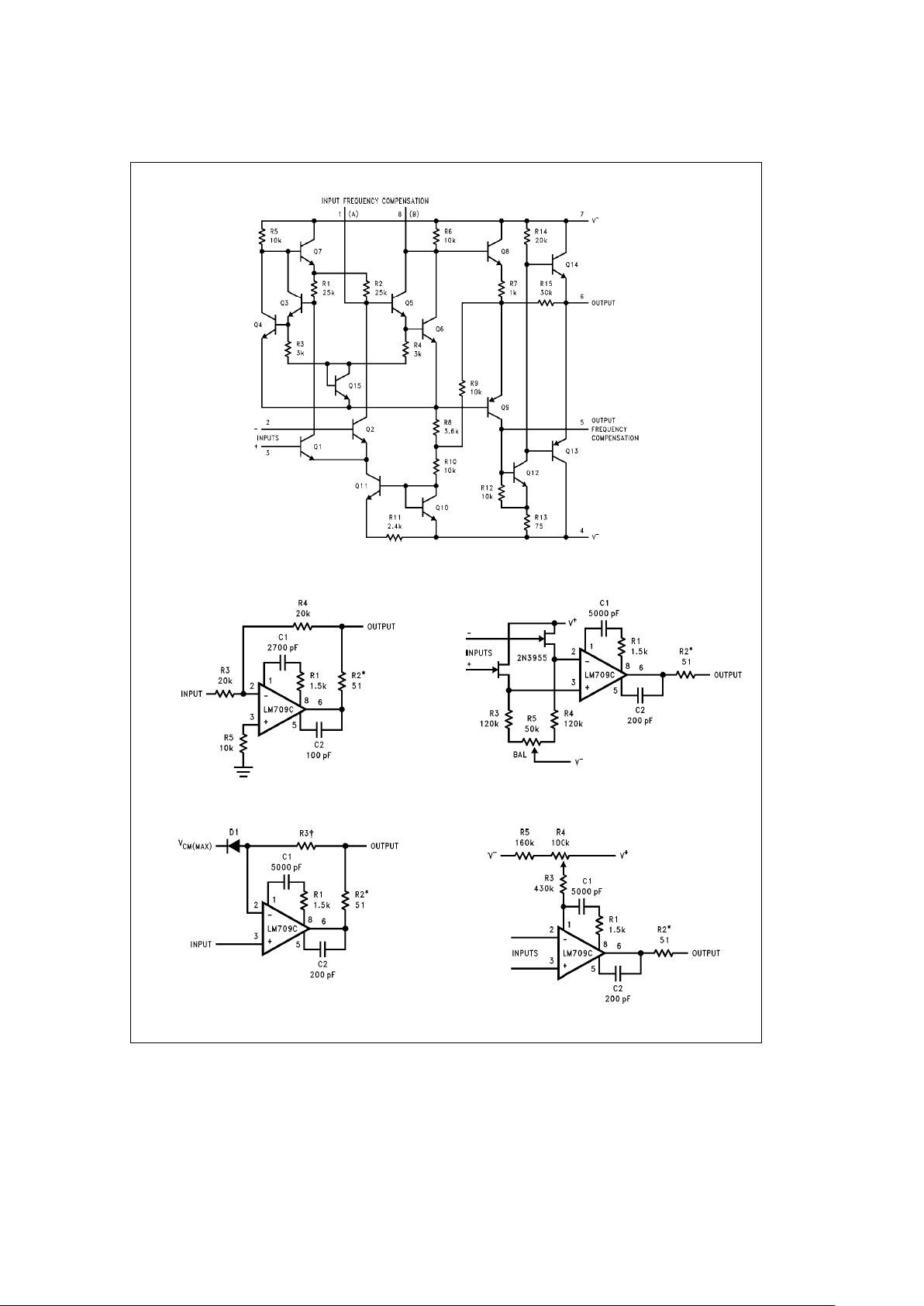
Schematic Diagram**
TL/H/11477– 1
Typical Applications**
Unity Gain Inverting Amplifier
TL/H/11477– 2
FET Operational Amplifier
TL/H/11477– 3
Voltage Follower
TL/H/11477– 7
*To be used with any capacitive loading on output.
**Pin connections shown are for metal can package.
²
Should be equal to DC source resistance on input.
Offset Balancing Circuit
TL/H/11477– 8
3
Page 4

Guaranteed Performance Characteristics
Output Voltage Swing Voltage Range
Input Common-Mode
Voltage Gain
Supply Current
TL/H/11477– 9
4
Page 5

Typical Performance Characteristics
Input Offset Current Input Bias Current Supply Current
Slew Rate as a Function of
Closed-Loop Gain Using
Recommended Compensation Networks
Various Closed-Loop Gains
Frequency Response for
as a Function of Frequency
Output Voltage Swing
Output Voltage Swing Supply Voltage
as a Function of
Input Bias Current
TL/H/11477– 10
5
Page 6

6
Page 7

Physical Dimensions inches (millimeters)
Metal Can Package (H)
Order Number LM709AH, LM709H or LM709CH
NS Package Number H08C
8-Lead Molded Dual-In-Line Package (N)
Order Number LM709CN-8
NS Package Number N08E
7
Page 8

LM709 Operational Amplifier
Physical Dimensions inches (millimeters) (Continued)
14-Lead Molded Dual-In-Line Package (N)
Order Number LM709CN
NS Package Number N14A
LIFE SUPPORT POLICY
NATIONAL’S PRODUCTS ARE NOT AUTHORIZED FOR USE AS CRITICAL COMPONENTS IN LIFE SUPPORT
DEVICES OR SYSTEMS WITHOUT THE EXPRESS WRITTEN APPROVAL OF THE PRESIDENT OF NATIONAL
SEMICONDUCTOR CORPORATION. As used herein:
1. Life support devices or systems are devices or 2. A critical component is any component of a life
systems which, (a) are intended for surgical implant support device or system whose failure to perform can
into the body, or (b) support or sustain life, and whose be reasonably expected to cause the failure of the life
failure to perform, when properly used in accordance support device or system, or to affect its safety or
with instructions for use provided in the labeling, can effectiveness.
be reasonably expected to result in a significant injury
to the user.
National Semiconductor National Semiconductor National Semiconductor National Semiconductor
Corporation Europe Hong Kong Ltd. Japan Ltd.
1111 West Bardin Road Fax: (
a
49) 0-180-530 85 86 13th Floor, Straight Block, Tel: 81-043-299-2309
Arlington, TX 76017 Email: cnjwge@tevm2.nsc.com Ocean Centre, 5 Canton Rd. Fax: 81-043-299-2408
Tel: 1(800) 272-9959 Deutsch Tel: (
a
49) 0-180-530 85 85 Tsimshatsui, Kowloon
Fax: 1(800) 737-7018 English Tel: (
a
49) 0-180-532 78 32 Hong Kong
Fran3ais Tel: (
a
49) 0-180-532 93 58 Tel: (852) 2737-1600
Italiano Tel: (
a
49) 0-180-534 16 80 Fax: (852) 2736-9960
National does not assume any responsibility for use of any circuitry described, no circuit patent licenses are implied and National reserves the right at any time without notice to change said circuitry and specifications.
 Loading...