

Page 1
LM675
Power Operational Amplifier
General Description
The LM675 is a monolithic power operational amplifier featuring widebandwidth and low input offset voltage, making it
equally suitable for AC and DC applications.
The LM675 iscapable of delivering outputcurrents in excess
of 3 amps,operating at supply voltages of up to 60V.The device overload protection consists of both internal current limiting and thermal shutdown. The amplifier is also internally
compensated for gains of 10 or greater.
Features
n 3A current capability
n A
typically 90 dB
VO
n 5.5 MHz gain bandwidth product
n 8 V/µs slew rate
n Wide power bandwidth 70 kHz
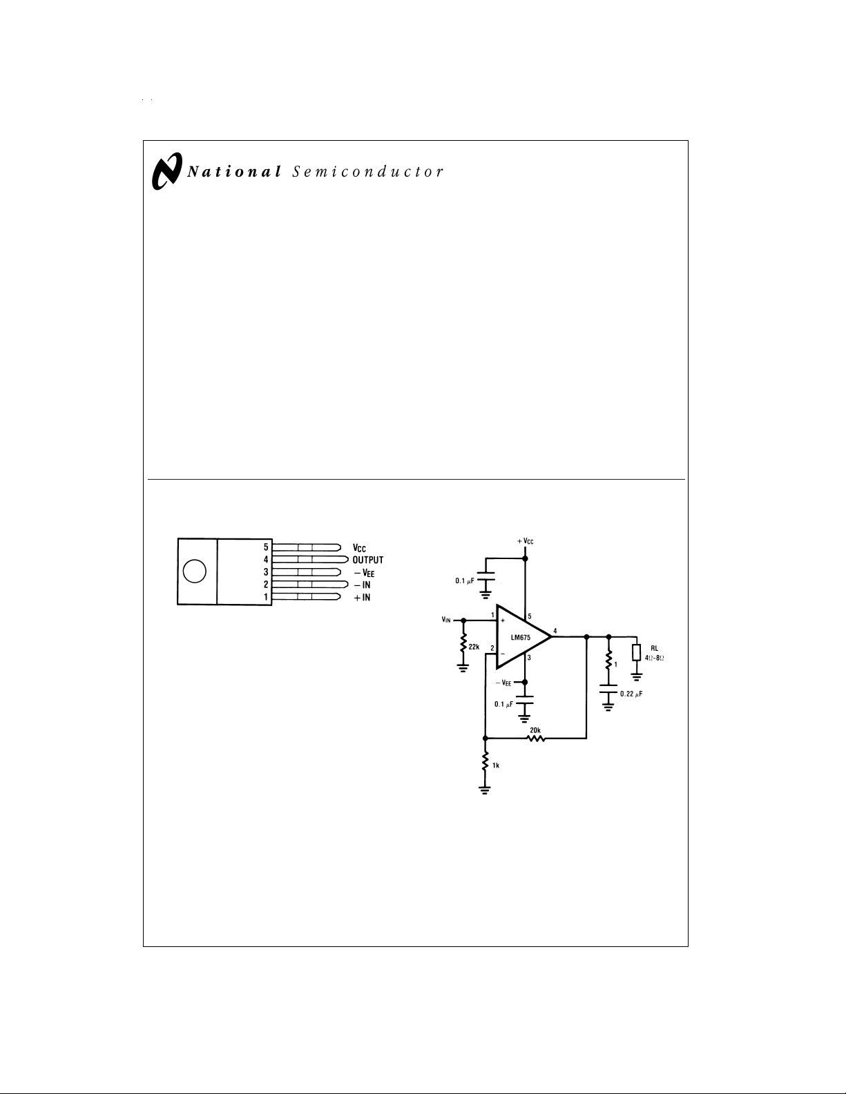
Connection Diagram Typical Applications
n 1 mV typical offset voltage
n Short circuit protection
n Thermal protection with parole circuit (100%tested)
n 16V–60V supply range
n Wide common mode range
n Internal output protection diodes
n 90 dB ripple rejection
n Plastic power package TO-220
Applications
n High performance power op amp
n Bridge amplifiers
n Motor speed controls
n Servo amplifiers
n Instrument systems
LM675 Power Operational Amplifier
May 1999
TO-220 Power Package (T)
*
The tab is internally connected to pin 3 (−VEE)
Front View
Order Number LM675T
See NS Package T05D
Non-Inverting Amplifier
DS006739-1
DS006739-2
© 1999 National Semiconductor Corporation DS006739 www.national.com
Page 2
Absolute Maximum Ratings (Note 1)
If Military/Aerospace specified devices are required,
please contact theNational Semiconductor Sales Office/
Distributors for availability and specifications.
Supply Voltage
Input Voltage −V
±
30V
to V
EE
Storage Temperature −65˚C to +150˚C
Junction Temperature 150˚C
Power Dissipation (Note 2) 30W
Lead Temperature
(Soldering, 10 seconds) 260˚C
ESD rating to be determined.
CC
Operating Temperature 0˚C to +70˚C
Electrical Characteristics
=
V
S
Supply Current P
Input Offset Voltage V
Input Bias Current V
Input Offset Current V
Open Loop Gain R
PSRR ∆V
CMRR V
Output Voltage Swing R
Offset Voltage Drift Versus Temperature R
Offset Voltage Drift Versus Output Power 25 µV/W
Output Power THD=1%,f
Gain Bandwidth Product f
Max Slew Rate 8 V/µs
Input Common Mode Range
Note 1: AbsoluteMaximumRatingsindicatelimitsbeyondwhich damage to the device may occur. Operating Ratings indicate conditions for which the device is functional, but do not guarantee specific performance limits. Electrical Characteristics state DC and AC electrical specifications under particular test conditions which guarantee specific performance limits. This assumes that the device is within the Operating Ratings. Specifications are not guaranteed for parameters where no limit is
given, however, the typical value is a good indication of device performance.
Note 2: Assumes T
±
25V, T
=
25˚C unless otherwise specified.
A
Parameter Conditions Typical Tested Limit Units
=
0W 18 50 (max) mA
OUT
=
0V 1 10 (max) mV
CM
=
0V 0.2 2 (max) µA
CM
=
0V 50 500 (max) nA
CM
=
∞
Ω 90 70 (min) dB
L
=
±
5V 90 70 (min) dB
S
=
±
20V 90 70 (min) dB
IN
=
8Ω
L
<
100 kΩ 25 µV/˚C
S
=
1 kHz, R
20 kHz, A
O
VCL
=
O
equal to 70˚C. For operation at higher tab temperatures, the LM675 must be derated based on a maximum junction temperature of 150˚C.
A
=
8Ω 25 20 W
L
=
1000 5.5 MHz
±
21
±
22
±
18 (min) V
±
20 (min) V
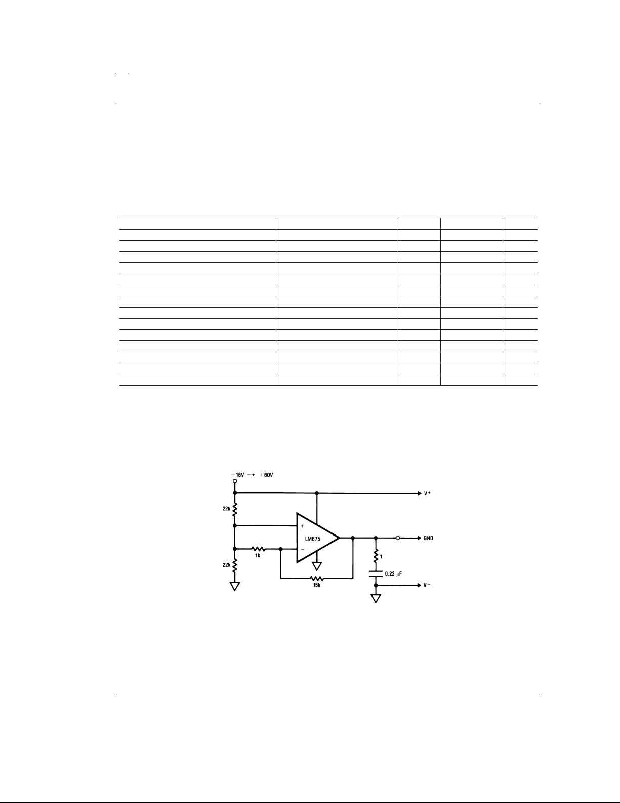
Typical Applications
Generating a Split Supply From a Single Supply
=
→
±
V
S
www.national.com 2
±
8V
30V
DS006739-3
Page 3
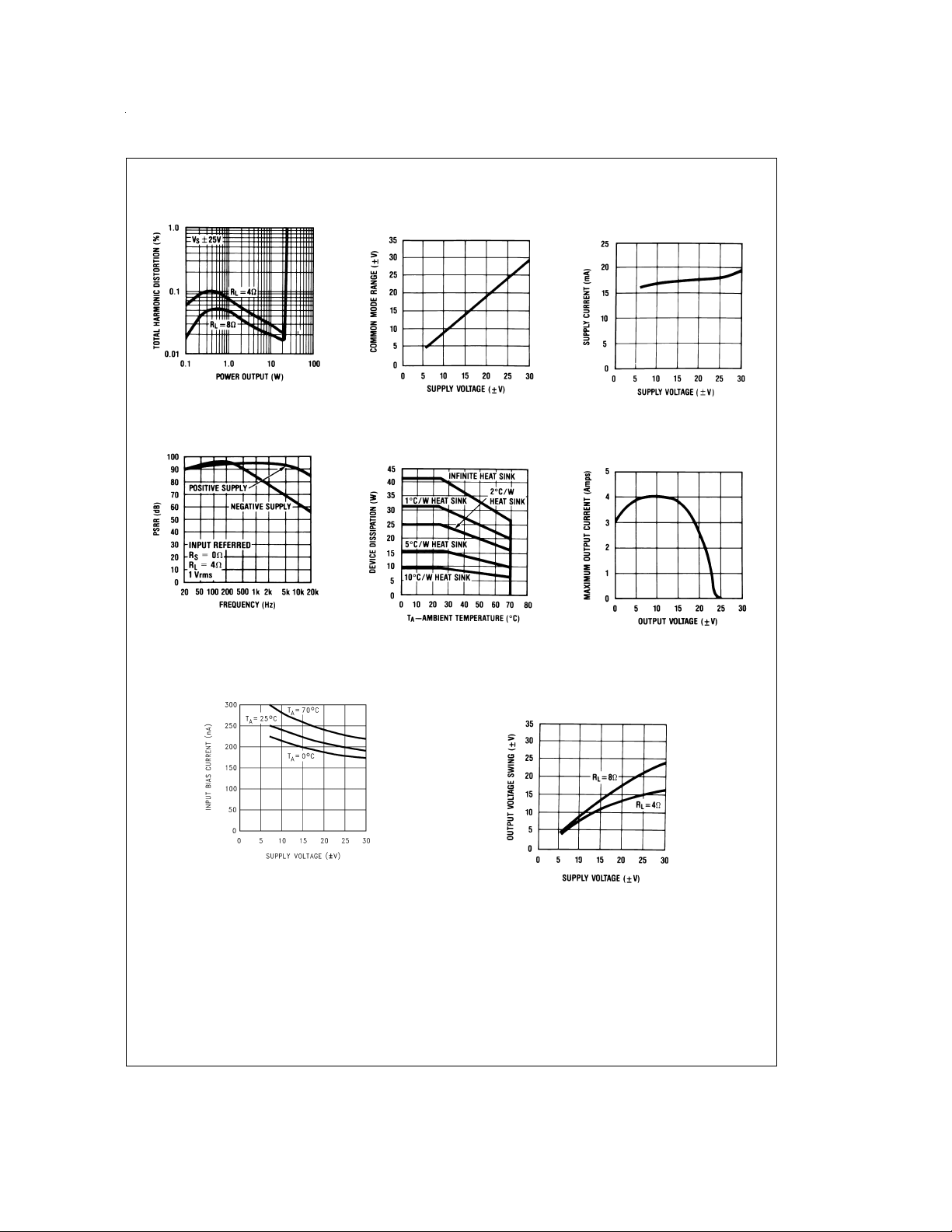
Typical Performance Characteristics
THD vs Power Output
PSRR vs Frequency
DS006739-10
DS006739-13
Input Common Mode
Range vs Supply Voltage
Device Dissipation vs
Ambient Temperature
†
θ INTERFACE=1˚ C/W
See Application Hints.
†
DS006739-11
DS006739-14
Supply Current vs
Supply Voltage
Current Limit vs
Output Voltage
=
±
*
V
S
*
25V
DS006739-12
DS006739-15
IBvs Supply Voltage
Output Voltage
Swing vs Supply Voltage
DS006739-16
DS006739-17
www.national.com3
Page 4

Schematic Diagram
DS006739-5
www.national.com 4
Page 5

Application Hints
STABILITY
The LM675 is designed to be stable when operated at a
closed-loop gain of 10 or greater, but, as with any other
high-current amplifier, the LM675 can be made to oscillate
under certain conditions. These usually involve printed circuit board layout or output/input coupling.
When designing a printed circuit board layout, it is important
to return the load ground, the output compensation ground,
and the low level (feedback and input) grounds to the circuit
board ground pointthrough separate paths. Otherwise, large
currents flowing along a ground conductor will generate voltages on the conductor which can effectively actas signals at
the input, resulting in high frequency oscillation or excessive
distortion. It is advisable to keep the output compensation
components and the 0.1 µF supply decoupling capacitors as
close as possible to the LM675 to reduce the effects of PCB
trace resistance and inductance. For the same reason, the
ground return paths for these components should be as
short as possible.
Occasionally, current in the output leads (which function as
antennas) can be coupled through the air to the amplifier input, resulting in high-frequency oscillation. This normally
happens when the source impedance is high or the input
leads are long. The problem can be eliminated by placing a
small capacitor (on the order of 50 pF to 500 pF) across the
circuit input.
Most power amplifiers do not drive highly capacitive loads
well, and the LM675 is no exception. If the output of the
LM675 is connected directly to a capacitor with no series resistance, the square wave response will exhibit ringing if the
capacitance is greater than about 0.1 µF. The amplifier can
typically drive load capacitances up to 2 µF or so withoutoscillating, but this is not recommended. If highly capacitive
loads are expected, a resistor (at least 1Ω) should be placed
in series with the output of the LM675. A method commonly
employed to protect amplifiers from low impedances at high
frequencies is to couple to the loadthrough a 10Ω resistor in
parallel witha5µHinductor.
CURRENT LIMIT AND SAFE OPERATING AREA
(SOA) PROTECTION
A power amplifier’s output transistors can be damaged by
excessive applied voltage,current flow, or powerdissipation.
The voltage applied tothe amplifieris limited by thedesign of
the external power supply, while the maximum current
passed by the output devices is usually limited by internal
circuitry to some fixed value. Short-term power dissipation is
usually not limited in monolithic operational poweramplifiers,
and this can be a problem whendriving reactive loads, which
may draw large currents while high voltages appear on the
output transistors. The LM675 not only limits current to
around 4A, but also reduces the value of the limit current
when an output transistor has a high voltage across it.
When driving nonlinear reactive loads such as motors or
loudspeakers with built-in protection relays, there is a possibility that an amplifier output will be connected to a load
whose terminal voltage may attempt to swing beyond the
power supply voltages applied to the amplifier. This can
cause degradation of the output transistors or catastrophic
failure of the whole circuit. The standard protection for this
type of failure mechanism is a pair of diodes connected be-
tween the output of the amplifier and the supply rails. These
are part of the internal circuitry of the LM675, and needn’t be
added externally when standard reactive loads are driven.
THERMAL PROTECTION
The LM675 has a sophisticated thermal protection scheme
to prevent long-term thermal stress to the device. When the
temperature on the die reaches 170˚C, the LM675 shuts
down. It starts operating again when the die temperature
drops to about 145˚C, but if the temperature again begins to
rise, shutdown will occur at only 150˚C. Therefore, the device is allowed to heat up to a relatively high temperature if
the fault condition is temporary, but a sustained faultwill limit
the maximum die temperature to a lower value. This greatly
reduces the stresses imposed on the IC by thermal cycling,
which in turn improves its reliability under sustained fault
conditions. This circuitry is 100%tested without a heat sink.
Since the die temperature is directly dependent upon the
heat sink, the heat sink should be chosen for thermal resistance low enough that thermal shutdown will not be reached
during normal operaton. Using the best heat sink possible
within the cost and space constraints of the system will improve the long-term reliability of any power semiconductor.
POWER DISSIPATION AND HEAT SINKING
The LM675 should always be operated with a heat sink,
even though at idle worst case power dissipation will be only
1.8W (30 mA x 60V) which corresponds to a rise in die temperature of 97˚C above ambient assuming θ
a TO-220 package. This in itself will not cause the thermal
=
jA
54˚C/W for
protection circuitry to shutdown the amplifierwhen operating
at room temperature, but a mere 0.9W of additional power
dissipation will shut the amplifier down since T
crease from 122˚C (97˚C + 25˚C) to 170˚C.
will then in-
J
In order to determine the appropriate heat sink for a given
application, the power dissipation of the LM675 in that application must be known. When the load is resistive, the maximum average power that the IC will be required to dissipate
is approximately:
where VSis the total power supply voltage across the
LM675, R
power dissipation of the amplifier. The above equation is
is the load resistance and PQis the quiescent
L
only an approximationwhich assumes an“ideal” class Boutput stage and constant power dissipation in all other parts of
the circuit. As anexample, if the LM675 is operated on a 50V
power supply with a resistive load of 8Ω,it can develop up to
19W of internalpower dissipation. If the die temperature is to
remain below 150˚C for ambient temperatures up to 70˚C,
the total junction-to-ambient thermal resistance must beless
than
Using θ
face thermal resistance and the heat-sink-to-ambient ther-
=
2˚C/W, the sum of the case-to-heat sink inter-
JC
mal resistance must be less than 2.2˚C/W. The
case-to-heat-sink thermal resistance of the TO-220 package
varies with the mounting method used. A metal-to-metal interface will be about 1˚C/W if lubricated, and about 1.2˚C/W
if dry. If a mica insulator is used, the thermal resistance will
be about 1.6˚C/W lubricated and 3.4˚C/W dry. For this ex-
www.national.com5
Page 6

Application Hints (Continued)
ample, we assume a lubricated mica insulator between the
LM675 and the heat sink. The heat sink thermal resistance
must then be less than
4.2˚C/W − 2˚C/W − 1.6˚C/W=0.6˚C/W.
This is a rather large heat sink and may not be practical in
some applications. If a smaller heat sink is required for reasons of size or cost, there are two alternatives. The maximum ambient operating temperature can be restricted to
50˚C (122˚F), resulting in a 1.6˚C/W heat sink, or the heat
sink can be isolated from the chassis so the mica washer is
not needed. This will change the required heat sink to a
1.2˚C/W unit if the case-to-heat-sink interface is lubricated.
Typical Applications
Non-Inverting Unity Gain Operation
The thermal requirements can become more difficult when
an amplifier is driving a reactive load. For a given magnitude
of load impedance, a higher degree of reactance will cause
a higher level of power dissipation within the amplifier. As a
general rule, the power dissipation of an amplifier driving a
60˚ reactive load will be roughly that of the same amplifier
driving the resistive part of that load. For example, some reactive loads may at some frequency have an impedance
with a magnitude of 8Ω and a phase angle of 60˚. The real
part of this load will then be 8Ω x cos 60˚ or 4Ω, and the amplifier power dissipation willroughly follow the curveof power
dissipation with a 4Ω load.
DS006739-6
Inverting Unity Gain Operation
www.national.com 6
DS006739-7
Page 7

Typical Applications (Continued)
Servo Motor Control
DS006739-8
High Current Source/Sink
=
I
x 2.5 amps/volt
V
OUT
IN
=
i.e. I
1A when V
OUT
Trim pot for max R
OUT
DS006739-9
=
400 mV
IN
www.national.com7
Page 8

Physical Dimensions inches (millimeters) unless otherwise noted
LM675 Power Operational Amplifier
TO-220 Power Package (T)
Order Number LM675T
NS Package T05D
LIFE SUPPORT POLICY
NATIONAL’S PRODUCTS ARE NOT AUTHORIZED FOR USE AS CRITICAL COMPONENTS IN LIFE SUPPORT
DEVICES OR SYSTEMS WITHOUT THE EXPRESS WRITTEN APPROVAL OF THE PRESIDENT AND GENERAL
COUNSEL OF NATIONAL SEMICONDUCTOR CORPORATION. As used herein:
1. Life support devices or systems are devices or
systems which, (a) are intended for surgical implant
into the body, or (b) support or sustain life, and
whose failure to perform when properly used in
accordance with instructions for use provided in the
2. A critical component is any component of a life
support device or system whose failure to perform
can be reasonably expected to cause the failure of
the life support device or system, or to affect its
safety or effectiveness.
labeling, can be reasonably expected to result in a
significant injury to the user.
National Semiconductor
Corporation
Americas
Tel: 1-800-272-9959
Fax: 1-800-737-7018
Email: support@nsc.com
www.national.com
National does not assume any responsibility for use of any circuitry described, no circuit patent licenses are implied and National reserves the right at any time without notice to change said circuitry and specifications.
National Semiconductor
Europe
Fax: +49 (0) 1 80-530 85 86
Email: europe.support@nsc.com
Deutsch Tel: +49 (0) 1 80-530 85 85
English Tel: +49 (0) 1 80-532 78 32
Français Tel: +49 (0) 1 80-532 93 58
Italiano Tel: +49 (0) 1 80-534 16 80
National Semiconductor
Asia Pacific Customer
Response Group
Tel: 65-2544466
Fax: 65-2504466
Email: sea.support@nsc.com
National Semiconductor
Japan Ltd.
Tel: 81-3-5639-7560
Fax: 81-3-5639-7507
 Loading...