

Page 1
LM6125/LM6225/LM6325
High Speed Buffer
General Description
The LM6125 family of high speed unity gain buffers slew at
800 V/µsand have a small signal bandwidth of 50 MHz while
driving a 50Ω load. These buffers drive
do not oscillate while driving large capacitive loads. The
LM6125 contains unique features notfound inpower buffers;
these include current limit, thermal shutdown, electronic
shutdown, and an error flag that warns of fault conditions.
These buffers are built with National’s VIP
grated PNP) process which provides fast PNP transistors
that are true complements to the already fast NPN devices.
This advancedjunction-isolated process delivers high speed
performance without the need for complexand expensivedielectric isolation.
±
300 mA peak and
™
(Vertically Inte-
Features
n High slew rate: 800 V/µs
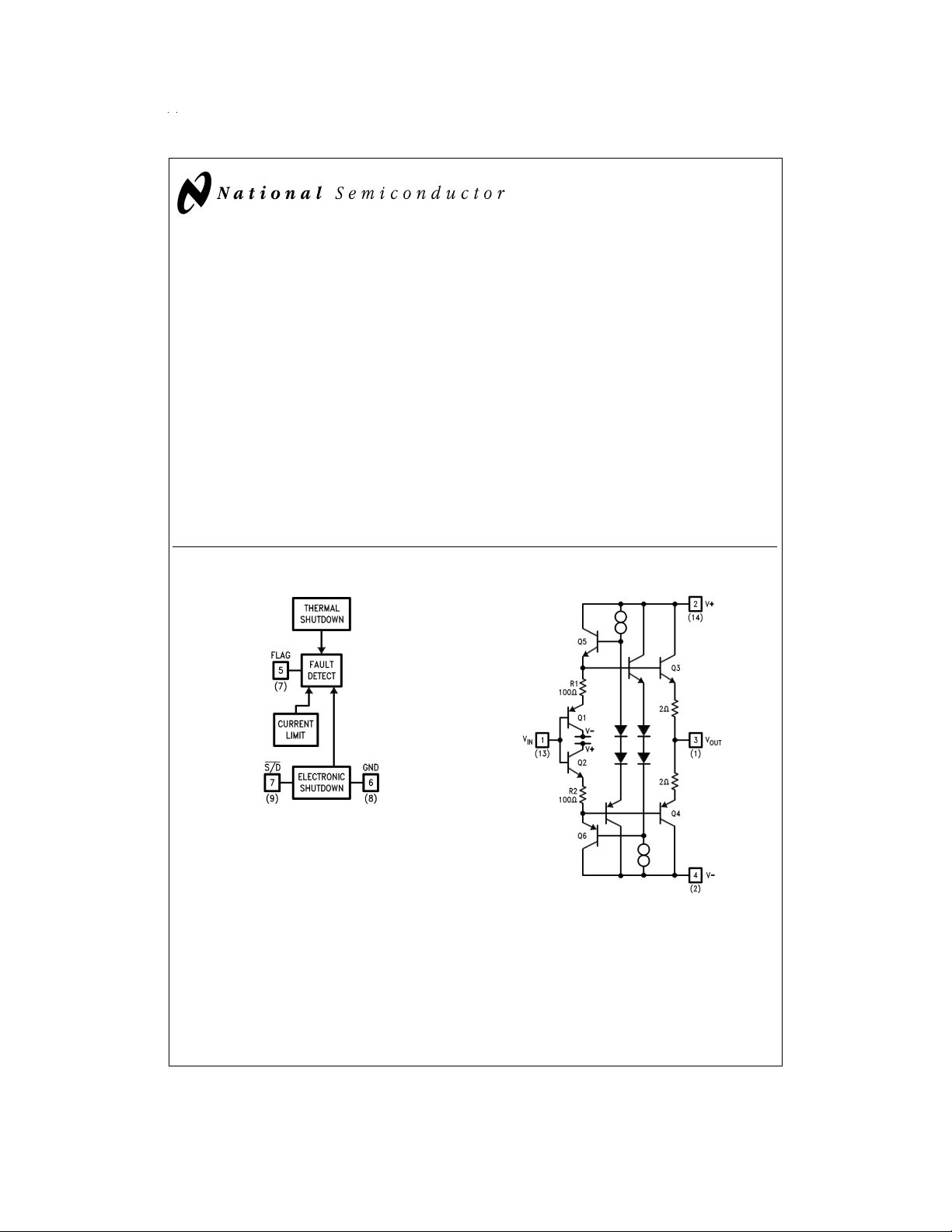
Simplified Schematic and Block Diagram
n High output current:
n Stable with large capacitive loads
n Current and thermal limiting
n Electronic shutdown
n 5V to
n Fully specified to drive 50Ω lines
Applications
n Line Driving
n Radar
n Sonar
±
300 mA
±
15V operation guaranteed
LM6125/LM6225/LM6325 High Speed Buffer
December 1994
DS009222-1
DS009222-2
Numbers in () are for 14–pin N DIP.
VIP™is a trademark of National Semiconductor Corporation.
© 1999 National Semiconductor Corporation DS009222 www.national.com
Page 2
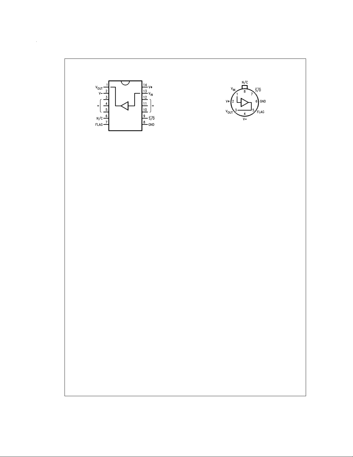
Pin Configurations
*Heat sinking pins.
Internally connected to V−.
Order Number LM6225N
See NS Package Number N14A
or LM6325N
DS009222-3
Note: Pin 4 connected to case
DS009222-4
Top View
Order Number LM6125H/883 (Note 1)
or LM6125H
See NS Package Number H08C
Note 1: Available per 5962-9081501
www.national.com 2
Page 3
Absolute Maximum Ratings (Note 2)
If Military/Aerospace specified devices are required,
please contact the National Semiconductor Sales Office/
Distributors for availability and specifications.
Supply Voltage 36V (
Input to Output Voltage (Note 2)
Input Voltage
Output Short-Circuit to GND
(Note 3) Continuous
Flag Output Voltage GND ≤ Vflag ≤ +Vsupply
Storage Temperature Range −65˚C to +150˚C
Lead Temperature
(Soldering, 10 seconds) 260˚C
±
±
Vsupply
18V)
±
7V
ESD Tolerance (Note 9)
(Note 4)
θ
JA
±
H Package 150˚C/W
N Package 40˚C/W
Maximum Junction
Temperature (T
) 150˚C
J
Operating Temperature Range
LM6125 −55˚C to +125˚C
LM6225 −40˚C to +85˚C
LM6325 0˚C to +70˚C
Operating Supply Voltage Range 4.75V to
1500V
±
16V
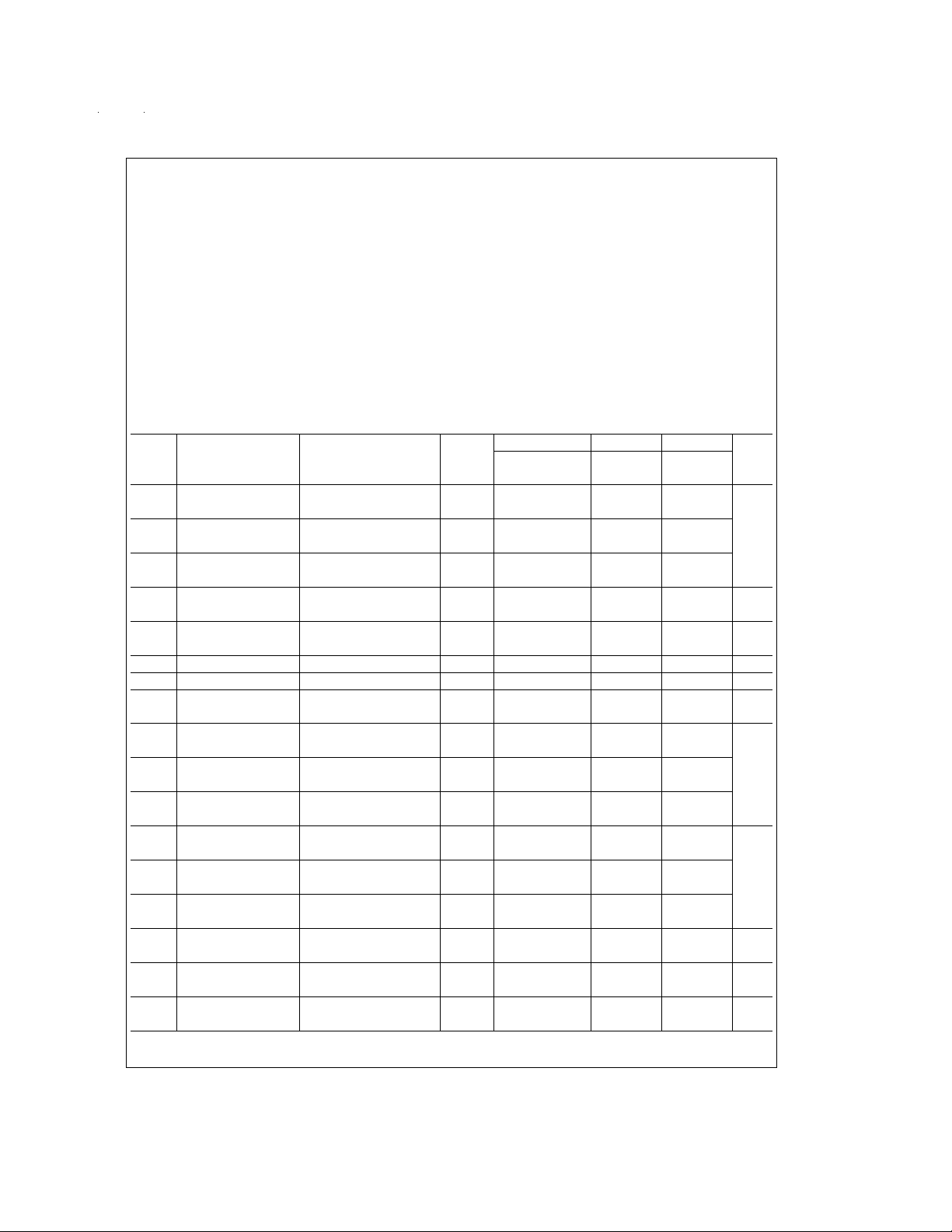
DC Electrical Characteristics
=
The following specifications apply for Supply Voltage
Boldface limits apply for T
=
=
T
A
to T
T
J
MIN
MAX
±
15V, V
; all other limits T
Symbol Parameter Conditions Typ LM6125 LM6225 LM6325 Units
OUT
=
L
=
L
=
L
=
IN
=
L
=
L
=
L
=
=
L
=
L
=
L
A
A
A
Voltage Gain 1 R
V1
Voltage Gain 2 R
V2
Voltage Gain 3 R
V3
(Note 6) V
V
I
R
C
R
I
I
I
Offset Voltage R
OS
Input Bias Current R
B
Input Resistance R
IN
Input Capacitance 3.5 pF
IN
Output Resistance I
O
Supply Current 1 R
S1
Supply Current 2 R
S2
Supply Current R
S/D
=
±
1kΩ,V
50Ω,V
10V 0.990 0.980 0.980 0.970
IN
=
±
10V 0.900 0.860 0.860 0.850 V/V
IN
50Ω,V+=5V 0.840 0.780 0.780 0.750
(1.5 VPP) 0.750 0.700 0.700
2V
PP
1kΩ 15 30 30 50 mV
1kΩ,R
=
10 kΩ 14 45µA
S
50Ω 5MΩ
±
10 mA 3 5 5 5 Ω
∞
∞
,V+=5V 14 16 16 18 mA
∞
±=±
,V
15V 1.1 1.5 1.5 1.5
in Shutdown 2.0 2.0 2.0
V
V
V
V
Output Swing 1 R
O1
Output Swing 2 R
O2
Output Swing 3 R
O3
Output Swing 4 R
O4
=
1kΩ 13.5 13.3 13.3 13.2
L
=
100Ω 12.7 11.5 11.5 11
L
=
50Ω 12 11 11 10
L
=
50Ω 1.8 1.6 1.6 1.6 V
L
PSRR Power Supply V+=5V (Note 6) 70 60 60 60 dB
Rejection Ratio 55 50 50 Min
V
Flag Pin Output V
OL
Low Voltage V
±=±
5V to±15V 300 300 340 mV
=
0V 400 400 400 Max
S/D
=
≥ 100 kΩ and R
0, R
CM
L
=
=
T
25˚C.
A
J
=
50Ω unless otherwise noted.
S
Limit Limit Limit
(Notes 5, 10) (Note 5) (Note 5)
0.970 0.950 0.950
0.800 0.820 0.820 Min
50 60 100 Max
777Max
10 10 6 Max
15 18 18 20
20 20 22
18 18 20 Max
13 13 13
10 10 10 Min
999
1.3 1.4 1.5 Min
±
PP
V
www.national.com3
Page 4

DC Electrical Characteristics (Continued)
=
The following specifications apply for Supply Voltage
Boldface limits apply for T
=
=
T
A
to T
T
J
MIN
MAX
±
15V, V
; all other limits T
Symbol Parameter Conditions Typ LM6125 LM6225 LM6325 Units
I
Flag Pin Output VOHFlag Pin=15V 0.01 10 10 10 µA
OH
High Current (Note 6) 20 20 20 Max
V
V
Shutdown Threshold 1.4 V
TH
Shutdown Pin 2.0 2.0 2.0 V
IH
Trip Point High 2.0 2.0 2.0 Min
V
Shutdown Pin 0.8 0.8 0.8 V
IL
Trip Point Low 0.8 0.8 0.8 Max
I
Shutdown Pin V
IL
=
0V −0.07 −10 −10 −10 µA
S/D
Input Low Current −20 −20 −20 Max
I
Shutdown Pin V
IH
=
5V −0.05 −10 −10 −10 µA
S/D
Input High Current −20 −20 −20 Max
I
O
Bi-State Output
Current
Shutdown Pin=0V 1 50 50 100 µA
=
V
+5V or −5V 2000 100 200
OUT
=
≥ 100 kΩ and R
0, R
CM
L
=
=
T
25˚C.
A
J
=
50Ω unless otherwise noted.
S
Limit Limit Limit
(Notes 5, 10) (Note 5) (Note 5)
AC Electrical Characteristics
=
The following specifications apply for Supply Voltage
Boldface limits apply for T
=
=
T
A
to T
T
J
MIN
MAX
±
15V, V
; all other limits T
Symbol Parameter Conditions Typ LM6125 LM6225 LM6325 Units
SR
SR
Slew Rate 1 V
1
Slew Rate 2 V
2
=
±
IN
=
±
IN
11V, R
11V, R
=
L
=
L
(Note 8)
SR
Slew Rate 3 V
3
=
2V
IN
PP,RL
=
V+=5V (Note 6)
R
V
R
IN
L
L
O
L
O
L
O
IN
L
=
100 mV
=
=
=
=
=
=
=
=
=
PP
≤10 pF Min
50Ω,C
L
≤10 pF 8.0 ns
50Ω,C
L
100 mV
PP
≤10 pF 4.0 ns
50Ω,C
L
100 mV
PP
≤10 pF 10
50Ω,C
L
100 mV
PP
, 1 MHz −50 dB
4V
PP
50Ω
BW −3 dB Bandwidth V
t
r,tf
Rise Time R
Fall Time V
t
PD
Propagation R
Delay Time V
O
S
V
FT
Overshoot R
VIN,V
Feedthrough Shutdown Pin=0V
OUT
in Shutdown V
C
OUT
Output Capacitance Shutdown Pin=0V 30 pF
in Shutdown
t
SD
Shutdown 700 ns
Response Time
Note 2: Absolute Maximum Ratings indicate limitsbeyond which damageto the device may occur. DC and ACelectrical specifications do not apply when operating
the device beyond its rated operating conditions.
Note 3: During current limit,thermal limit, or electronicshutdown the input current willincrease if the input tooutput differential voltage exceeds 8V. See Overvoltage
Protection in Application Hints.
Note 4: The LM6125 series buffers contain current limit and thermal shutdown to protect against fault conditions.
=
≥ 100 kΩ and R
0, R
CM
L
=
=
T
25˚C.
A
J
=
50Ω unless otherwise noted.
S
Limit Limit Limit
(Note 5) (Note 5) (Note 5)
1kΩ 1200 V/µs
50Ω 800 550 550 550
Min
50Ω 50
50 30 30 30 MHz
%
www.national.com 4
Page 5

AC Electrical Characteristics (Continued)
Note 5: For operation at elevated temperature, these devices must be derated based on a thermal resistance of θJAand TJmax, T
LM6125H and LM6225H is 17˚C/W. The thermal impedance θ
heat-sinking pins (pins 3, 4,5, 10, 11, and 12) are connectedto2 square inches of 2oz. copper.When installed in a socket,the thermal impedance θ
age is 60˚C/W.
Note 6: Limits are guaranteed by testing or correlation.
Note 7: The input is biased to +2.5V, and V
is reduced to 1.5 V
Note 8: The Error Flag is set (low) during currentlimit or thermalfault detection inaddition to beingset by theShutdown pin. Itis an open-collector output which re-
quires an external pullup resistor.
Note 9: Slew rate is measured with a
will be approximately
device heating. For slew rate versus junction temperature see typical performance curves. The input pulse amplitude should be reduced to
at temperature extremes. For accurate measurements, the input slew rate should be at least 1700 V/µs.
Note 10: The test circuit consists of the human body model of 120 pF in series with 1500Ω.
Note 11: A military RETS specificationis available on request.Atthe time of printing, the LM6125H/883 RETS spec complied with theBoldface limits in thiscolumn.
The LM6125H/883 may also be procured as Standard Military Drawing specification
.
PP
±
10V.Slewrateis calculated for transitions between±5V levels on both rising and fallingedges.Ahigh speedmeasurementisdone to minimize
swings VPPabout this value. The input swing is 2 VPPat all temperatures except for theAV3 test at −55˚C where it
IN
±
11V input pulse and 50Ω source impedance at 25˚C. Since voltage gainis typically 0.9 driving a 50Ω load, the output swing
of the device in the N package is 40˚C/W when soldered directly to a printed circuit board, and the
JA
#
5962-9081501MXX.
=
+ θJAPD. θJCfor the
T
J
A
JA
±
10V for measurements
of the N pack-
Typical Performance Characteristics T
Frequency Response
DS009222-9
Overshoot vs Capacitive Load
DS009222-12
Frequency Response
Large Signal Response
=
(R
1kΩ)
L
= 25˚C, VS=±15V unless otherwise specified
A
Slew Rate vs Temperature
DS009222-10
Large Signal Response
=
(R
50Ω)
L
DS009222-13
DS009222-11
DS009222-14
Supply Current
DS009222-15
−3 dB Bandwidth
DS009222-16
Slew Rate
DS009222-17
www.national.com5
Page 6

Typical Performance Characteristics T
= 25˚C, VS=±15V unless otherwise specified (Continued)
A
Slew Rate
DS009222-18
Power Bandwidth
Forward Transmission
Gain (S21)
DS009222-21
Typical Connection Diagram
Input Return Gain
(S11)
DS009222-19
DS009222-20
Current Limit
DS009222-22
www.national.com 6
DS009222-6
Page 7

Application Hints
POWER SUPPLY DECOUPLING
The method of supply bypassing is not critical for stability of
the LM6125 series buffers. However, their high current output combined with high slew rate can result in significant
voltage transients on the power supply lines if much inductance is present. For example,a slew rate of 900 V/µs into a
50Ω load produces a di/dt of 18 A/µs. Multiplying this by a
wiring inductance of 50 nH results in a 0.9V transient. To
minimize this problem use high qualitydecoupling veryclose
to thedevice. Suggested values are a 0.1 µF ceramic in parallel withone or two 2.2 µFtantalums. A ground plane is recommended.
LOAD IMPEDANCE
The LM6125 is stable into any load when driven by a 50Ω
source. As shown in the
graph, worst case is a purely capacitive load of about
1000 pF. Shunting the load capacitance with a resistor will
reduce overshoot.
SOURCE INDUCTANCE
Like any high-frequency buffer, the LM6125 can oscillate at
high values of source inductance. The worst case condition
occurs at a purely capacitive load of 50 pF where up to
100 nH of source inductance can be tolerated. With a 50Ω
load, this goes up to 200 nH.This sensitivitymay bereduced
at the expense ofa slightreduction inbandwidth by adding a
resistor in series with thebuffer input. A 100Ωresistor will ensure stability with source inductances up to 400 nH with any
load.
ERROR FLAG LOGIC
The Error Flag pinis anopen-collector output which requires
an external pull-up resistor. Flag voltage is HIGH during operation, andis LOW during a fault condition. A faultcondition
occurs if either the internal current limit or the thermal shut-
Overshoot vs Capacitive Load
down isactivated, or the shutdown (S/D) pin is driven low by
external logic. Flag voltage returns to its HIGH state when
normal operation resumes.
If theS/D pin is not tobe used, it should beconnected to V
OVERVOLTAGE PROTECTION
The LM6125 may be severely damaged or destroyed if the
Absolute Maximum Rating of 7V between input and output
pins is exceeded.
If thebuffer’s input-to-output differential voltage isallowed to
exceed 7V, a base-emitter junction will be in
reverse-breakdown, and will be in series with a
forward-biased base-emitter junction. Referring to the
LM6125 simplified schematic, the transistors involved are
Q1 and Q3 for positive inputs, and Q2 and Q4 for negative
inputs. If any current is allowed to flow through these junctions, localized heating of the reverse-biased junction will occur, potentially causing damage. The effectof the damage is
typically increased offset voltage, increased bias current,
and/or degraded AC performance. The damage is cumulative, and may eventually result in complete device failure.
The device is best protected by the insertion of the parallel
combination of a 100 kΩ resistor (R1) and a small capacitor
(C1) in series with the buffer input, and a 100 kΩ resistor
(R2) from input to output of the buffer (see
Figure 1
). This
network normally has no effect on the buffer output. However,if thebuffer’s currentlimit orshutdown is activated, and
the output has a ground-referred load of significantly less
than 100 kΩ, a large input-to-output voltage may bepresent.
R1 and R2 then form a voltage divider, keeping the
input-output differential below the 7V Maximum Rating for input voltages up to 14V. This protection network should be
sufficient to protectthe LM6125from theoutput of nearly any
op amp which is operated on supply voltages of
±
15V or
lower.
+
.
DS009222-8
FIGURE 1. LM6125 with Overvoltage Protection
www.national.com7
Page 8

Physical Dimensions inches (millimeters) unless otherwise noted
Order Number LM6125H/883 or LM6125H
Metal Can Package (H)
NS Package Number H08C
Molded Dual-In-Line Package (N)
Order Number LM6225N or LM6325N
NS Package Number N14A
www.national.com 8
Page 9

Notes
LM6125/LM6225/LM6325 High Speed Buffer
LIFE SUPPORT POLICY
NATIONAL’S PRODUCTS ARE NOT AUTHORIZED FOR USE AS CRITICAL COMPONENTS IN LIFE SUPPORT
DEVICES OR SYSTEMS WITHOUT THE EXPRESS WRITTEN APPROVAL OF THE PRESIDENT OF NATIONAL
SEMICONDUCTOR CORPORATION. As used herein:
1. Life support devices or systems are devices or
systems which, (a) are intended for surgical implant
into the body, or (b) support or sustain life, and
whose failure to perform when properly used in
accordance with instructions for use provided in the
2. A critical component is any component of a life
support device or system whose failure to perform
can be reasonably expected to cause the failure of
the life support device or system, or to affect its
safety or effectiveness.
labeling, can be reasonably expected to result in a
significant injury to the user.
National Semiconductor
Corporation
Americas
Tel: 1-800-272-9959
Fax: 1-800-737-7018
Email: support@nsc.com
www.national.com
National does not assume any responsibility for use of any circuitry described, no circuit patent licenses are implied and National reserves the right at any time without notice to change said circuitry and specifications.
National Semiconductor
Europe
Fax: +49 (0) 1 80-530 85 86
Email: europe.support@nsc.com
Deutsch Tel: +49 (0) 1 80-530 85 85
English Tel: +49 (0) 1 80-532 78 32
Français Tel: +49 (0) 1 80-532 93 58
Italiano Tel: +49 (0) 1 80-534 16 80
National Semiconductor
Asia Pacific Customer
Response Group
Tel: 65-2544466
Fax: 65-2504466
Email: sea.support@nsc.com
National Semiconductor
Japan Ltd.
Tel: 81-3-5639-7560
Fax: 81-3-5639-7507
 Loading...