

Page 1
LM6313 High Speed,
High Power Operational Amplifier
LM6313 High Speed, High Power Operational Amplifier
February 1995
General Description
The LM6313 is a high-speed, high-power operational amplifier. This operational amplifier features a 35 MHz small signal bandwidth, and 250 V/ms slew rate. A compensation pin
is included for adjusting the open loop bandwidth. The input
stage (A1) and output stage (A2) are pinned out separately,
and can be used independently. The operational amplifier is
designed for low impedance loads and will deliver
g
300 mA. The LM6313 has both overcurrent and thermal
shutdown protection with an error flag to signal both these
fault conditions.
These amplifiers are built with National’s VIP
TM
(Vertically
Integrated PNP) process which provides fast PNP transistors that are true complements to the already fast NPN devices. This advanced junction-isolated process delivers high
speed performance without the need for complex and expensive dielectric isolation.
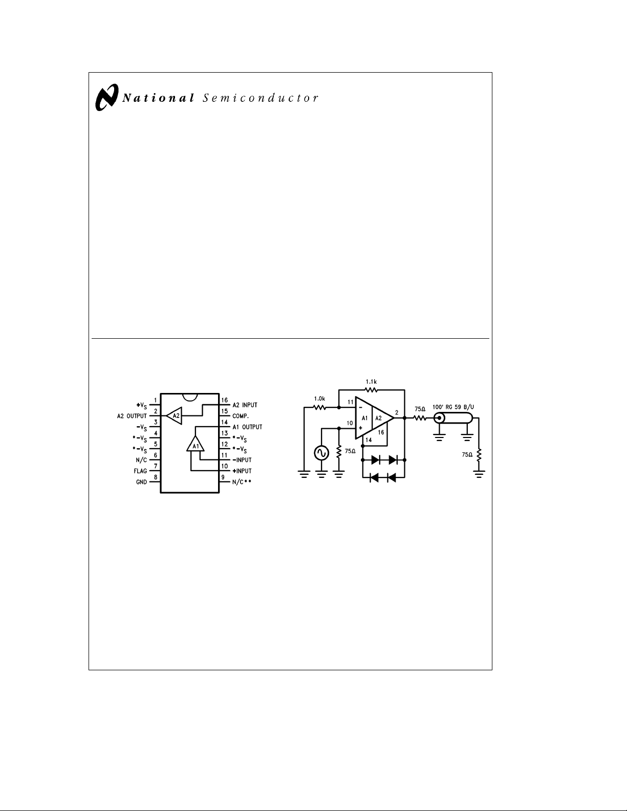
Connection Diagram
Dual-In-Line Package
Features
Y
High slew rate 250 V/ms
Y
Wide bandwidth 35 MHz
Y
Peak output current
Y
Input and output stages pinned out separately
Y
Single or dual supply operation
Y
Thermal protection
Y
Error flag warns of faults
Y
Wide supply voltage range
g
300 mA
g
5V tog15V
Applications
Y
High speed ATE pin driver
Y
Data acquisition
Y
Driving capacitive loads
Y
Flash A-D input driver
Y
Precision 50X –75X video line driver
Y
Laser diode driver
Typical Application
TL/H/10521– 2
TL/H/10521– 1
Top View
Order Number LM6313N
See NS Package Number N16A
*Heat sink pins
See Note 5 and Applications.
**Do not ground or otherwise connect to this pin.
VIPTMis a trademark of National Semiconductor Corporation.
C
1995 National Semiconductor Corporation RRD-B30M75/Printed in U. S. A.
TL/H/10521
Page 2
Absolute Maximum Ratings (Note 1)
a
Total Supply Voltage (
A1 Differential Input Voltage (Note 2)
A1 Input Voltage (V
A2 Input to Output Voltage
A2 Input Voltage
Flag Output Voltage GND toaV
Short-Circuit to Ground (Note 3)
Storage Temperature Range
VStobVS) 36V (g18)
g
a
b
b
65§CsT
0.7) to (V
7V
b
b
7V)
g
7V
g
V
s
a
150§C
Lead Temperature (Soldering, 5 seconds) 260
ESD Tolerance (Note 4)
Pins 10 and 11
All Other Pins
Operating Temperature Range
S
S
LM6313N 0
Thermal Derating Information (Note 5)
i
JA
T
(Max) 125§C
J
g
600V
g
1500V
Cto70§C
§
40§C/W
C
§
Operational Amplifier DC Electrical Characteristics Unless otherwise specified, all limits
guaranteed for T
e
R
50X, the circuit configured as in
S
Symbol Parameter Conditions Typical
V
OS
DVOS/DT Average Input Offset
I
b
I
OS
DIOS/DT Average Input Offset
R
IN
C
IN
V
CM
A
V1
A
V2
CMRR Common-Mode
PSRR Power Supply
V
O1
V
O2
V
O3
I
S
I
SC
e
25§C, and Supply Voltage V
A
Figure 1
e
g
15V. Boldface limits apply at temperature extremes. V
S
.
C0
25
§
Cto70§C
§
Limit Limit
CM
e
Units
Input Offset Voltage 5 20 22 mV (Max)
Voltage Drift
10 mV/
Input Bias Current 2 5 7 mA (Max)
Input Offset Current 0.15 1.5 1.9 mA (Max)
Current Drift
0.4 nA/
§
Input Resistance Differential 325 kX
Input Capacitance A
Common-Mode
Voltage Range
Voltage Gain 1 R
Voltage Gain 2 R
Rejection Ratio
Rejection Ratio
Output Voltage Swing 1 R
Output Voltage Swing 2 R
Output Voltage Swing 3 R
Supply Current T
Peak Short-Circuit Output (See
ea
1, fe10 MHz 2.2 pF
V
a
14.2
b
13.2
e
L
e
L
b
10VsV
g
5VsV
e
L
e
L
e
L
e
0§C 24
J
e
T
25§C 18 23 mA (Max)
J
e
T
125§C 21
J
Figure 3
e
1kX,V
50X,V
g
10V 6000 2500 2000
O
e
g
8V 5000 2000 1500
O
s
a
10V
CM
s
g
16V
S
90 72 70 dB (Min)
90 72 70 dB (Min)
1kX 13.1 11.8 11.2
100X 12.0 10.5 10.0
50X 11.0 9.0 8.5
) 300 mA
a
13.8
b
12.8
a
b
13.7
12.7
V (Min)
V/V (Min)
g
V (Min)
0V,
C
§
C
FIGURE 1
2
TL/H/10521– 3
Page 3
Electrical Characteristics (Continued)
Operational Amplifier AC Electrical Characteristics Unless otherwise specified, all limits
guaranteed for T
e
R
50X, the circuit configured as in
S
e
25§C, and Supply Voltage V
A
Figure 1
e
g
15V. Boldface limits apply at temperature extremes. V
S
.
CM
e
Symbol Parameter Conditions Typical Units
GBW Gain-Bandwidth Product
SR Slew Rate A
PBW Power Bandwidth V
t
S
Settling Time 10V Step to 0.1% (See
Phase Margin A
@
fe30 MHz 35 MHz
V
OUT
V
eb
eb
e
1, R
50X (Note 6) 250 V/ms
L
e
20 V
1, R
L
PP
e
1kX,C
Figure 2
) 200 ns
e
50 pF 53 Deg
L
3.0 MHz
Differential Gain 0.1 %
Differential Phase 0.1 Deg
e
n
i
n
A1 DC Electrical Characteristics Unless otherwise specified, all limits guaranteed for T
Supply Voltage V
Symbol Parameter Conditions Typical
A
VOL
CMRR Common-Mode
PSRR Power Supply
I
SC
Input Noise Voltage fe10 kHz 14 nV/SHz
Input Noise Current fe10 kHz 1.8 pA/SHz
e
g
15V. Boldface limits apply at temperature extremes. V
S
CM
e
0V, R
25
e
50X.
S
C0
§
Cto70§C
§
Limit Limit
Large Signal Voltage Gain V
Rejection Ratio
Rejection Ratio
Output Short
Circuit Current
OUT
V
OUT
b
10VsV
g
5V
e
g
e
g
s
g
10V, R
10V, R
CM
s
V
S
e
2kX 650 300 250
L
e %
L
s
a
10V
a
16V
6000 2500 2000
90 72 70 dB (Min)
90 72 70 dB (Min)
g
60
g
30
g
25 mA (Min)
A
e
25§C, and
V/V (Min)
Units
0V,
A1 AC Electrical Characteristics Unless otherwise specified, all limits guaranteed for T
Supply Voltage V
Symbol Parameter Conditions Typical
e
g
15V. Boldface limits apply at temperature extremes. R
S
e
50X.
S
25
§
Limit
e
25§C, and
A
C Units
GBW Gain-Bandwidth fe30 MHz 37 25 MHz (Min)
e
1500X.
ea
V
g
2V
SR Slew Rate A
Note 1: Absolute Maximum Ratings indicate limits beyond which damage to the device may occur. For guaranteed specifications and test conditions, see the
Electrical Characteristics. The guaranteed specifications apply only for the test condition listed. Some performance characteristics may degrade when the device is
not operated under the listed test conditions.
Note 2: In order to achieve optimum AC performance, the input stage was designed without protective clamps. Exceeding the maximum differential input voltage
results in reverse breakdown of the base-emitter junction of one of the input transistors. Degradation of the input parameters (especially V
proportional to the level of the externally limited breakdown current and the accumulated duration of the breakdown condition.
Note 3: Continuous short-circuit operation of A1 at elevated temperature can result in exceeding the maximum allowed junction temperature of 125
current limit and thermal shutdown to protect against fault conditions. The device may be damaged by shorts to the supplies.
Note 4: Human body model, C
e
100 pF, R
S
OUT
1, R
L
e
100 kX,g4VIN,
250 150 V/ms (Min)
, and Noise) is
OS,IOS
C. A2 contains
§
3
Page 4

Electrical Characteristics (Continued)
A2 DC Electrical Characteristics Unless otherwise specified, all limits guaranteed for T
Supply Voltage V
Symbol Parameter Conditions Typical
A
V1
A
V2
V
OS
I
b
R
IN
C
IN
R
O
V
O
PSRR Power Supply V
A2 AC Electrical Characteristics Unless otherwise specified, all limits guaranteed for T
Supply Voltage V
Symbol Parameter Conditions Typical
SR 1 Slew Rate 1 V
SR 2 Slew Rate 2 V
BW
tr, Rise Time R
t
f
P
D
e
g
15V. Boldface limits apply at temperature extremes. R
S
e
50X.
S
C0
25
§
Cto70§C
§
Limit Limit
Voltage Gain 1 R
Voltage Gain 2 R
Offset Voltage R
Input Bias Current R
Input Resistance R
e
1kX,V
L
e
50X,V
L
e
1kX 15 70 100 mV (Max)
L
e
1kX,R
L
e
50X 5MX
L
e
g
10V 0.99 0.97 0.95 V/mV (Min)
IN
e
g
10V 0.9 0.85 0.82 V/V (Min)
IN
e
10 kX 16 8 mA (Max)
S
Input Capacitance 3.5 pF
e
Output Resistance I
Voltage Output Swing R
Rejection Ratio
e
g
15V. Boldface limits apply at temperature extremes. R
S
g
OUT
R
R
10 mA 3.5 5.0 8.0 X (Min)
e
1kX 13.7 13.0 12.7
L
e
100X 12.5 10.5 10.0 V (Min)
L
e
50X 11.0 9.0 8.5
L
e
g
5V tog16V
S
70 60 50 dB (Min)
e
50X.
S
C
25
§
Limit
b
3 dB Bandwidth V
Fall Time V
Propagation Delay R
Overshoot R
e
g
IN
e
g
IN
e
g
IN
e
R
50X,C
L
e
1kX,C
L
e
100 mVpp
O
e
50X,C
L
e
V
100 mVpp
O
e
1kX,C
L
e
R
50X,C
L
e
11V, R
11V, R
1kX 1200
L
e
50X (Note 7) 750 550
L
100 mVpp
s
10 pF
L
s
10 pF
L
s
10 pF
L
e
100 pF 13
L
e
1000 pF 21
L
65 30 MHz (Min)
8ns
4ns
e
A
e
A
V/ms (Min)
25§C, and
Units
25§C, and
Units
%
Additional (A2) Electrical Characteristics Unless otherwise specified, all limits guaranteed for
e
T
25§C, and Supply Voltage V
A
Symbol Parameter Conditions Typical
V
OL
I
OH
Note 5: For operation at elevated temperature, these devices must be derated to insure T
to the PCB, is 40
Note 6: Measured between
Note 7: V
Note 8: The error flag is set during current limit or thermal shut-down. The flag is an open collector, low on fault.
Flag Pin Output I
Low Voltage
Flag Pin Output VOHFlag Pine15V (Note 8)
High Current
C/W when pins 4, 5, 12 and 13 are soldered to a total of 2 in2of copper trace.
§
g
e
g
9V step input, measured betweeng5V out.
IN
5V.
e
g
15V. Boldface limits apply at temperature extremes.
S
Flag Pine500 mA
SINK
220 340 400 mV (Max)
0.01 10 20 mA (Max)
s
125§C. T
J
C0
25
§
Limit Limit
e
a
T
(P
J
A
D
Cto70§C
§
c
iJA). iJAfor the N package mounted flush
Units
4
Page 5

Simplified Schematic
Settling Time Test Circuit
TL/H/10521– 4
FIGURE 2
TL/H/10521– 5
Protection Circuit Block Diagram
TL/H/10521– 7
FIGURE 3
TL/H/10521– 6
5
Page 6

Typical Performance Characteristics Op Amp
(Unless otherwise specified, T
A
e
25§C, V
S
e
g
15V, and R
L
e
10 kX.)
Slew Rate vs
Capacitive Load
Bias Current vs
Common-Mode Voltage
Bode Plot (Open Loop)
Supply Current vs
Supply Voltage
Output Resistance
Power Supply Rejection
Slew Rate vs
Input Noise Voltage Input Noise Current Compensation
Gain-Bandwidth, Phase
Margin vs Comp Cap
and Load Cap
CMR vs Frequency vs Comp Cap
GBW and Phase Margin
TL/H/10521– 8
6
Page 7

Typical Performance Characteristics A1 Only
(Unless otherwise specified, T
e
A
25§C, V
S
e
g
15V, and R
L
e
10 kX.)
Gain vs Supply Voltage Bode Plot Load Capacity
Gain-Bandwidth and
Phase Margin vs
Output Saturation Voltage Saturation Voltage
Common-Mode Input
Typical Performance Characteristics A2 Only
(Unless otherwise specified, T
Slew Rate vs
Supply Voltage
e
A
25§C and V
e
g
15V.)
S
Slew Rate vs
Input Amplitude
Output Resistance
(Open Loop)
TL/H/10521– 9
Slew Rate vs
Temperature
Bandwidth vs
Supply Voltage
Overshoot vs
Capacitive Load
7
Gain and Phase
Shift (R
e
50X)
L
TL/H/10521– 10
Page 8

Application Hints
The LM6313 is a high-speed, high power operational amplifier that is designed for driving low-impedance loads such
as 50X and 75X cables. Available in the standard, low cost,
16-pin DIP, this amplifier will drive back terminated video
cables with up to 10 Vp-p. The ability to add additional compensation allows the LM6313 to drive capacitive loads of
any size at bandwidths previously possible only with very
expensive hybrid devices.
The LM6313 is excellent for driving high-speed flash A-to-D
converters that require low-impedance drive at high frequencies. At 1 MHz, when used as a buffer, the LM6313
output impedance is below 0.1X. This very low output impedance also means that cables can be accurately backterminated by just placing the characteristic impedance in
series with the LM6313 output.
OVER-VOLTAGE PROTECTION
If the LM6313 is being operated on supply voltages of great-
g
er than
transistors exists. At higher supply voltages, if the output is
shorted or excessive power dissipation causes the output
stage to shut down, the maximum A2 input-to-output voltage, can be exceeded. This occurs when the input stage
tries to drive the output while the output is at ground. To
prevent this from happening, an easy solution is to place
diodes around the output stage (See
limit the maximum differential voltage to about 1.3V. Any
signal diode, such as the 1N914 or the 1N4148 will work
fine.
HEAT SINKING
When driving a low impedance load such as 50X, and operating from
the LM6313 can rise above 3W. To prevent overheating of
the chip, which would cause the thermal protection circuitry
to shut the system down, the following guidelines should be
followed:
1. Reduce the supply voltage. The LM6313 will operate
2. Solder pins 4, 5, 12 and 13 to copper traces which are at
5V, the possibility of damaging the output stage
Figure 4
). This will
TL/H/10521– 11
FIGURE 4
g
15V supplies, the internal power dissipation of
with little change in performance, except output voltage
swing, on
g
5V supplies. This will reduce the dissipation
to the level where no precautions against overheating
are necessary for loads of 10X or more.
least 0.100 inch wide and have a total area of at least 2
square inches, to obtain a i
pins are connected to the back of the chip and will be at
b
V
. They should not be used as a Vbconnection un-
of 40§C/W. These four
JA
less pin 3 is also connected to this same point.
SUPPLY BYPASSING
Because of the large currents required to drive low-impedance loads, supply bypassing as close as possible to the
I.C. is important. At 50 MHz, a few inches of wire or circuit
trace can have 20X or 30X of inductive reactance. This
inductance in series with a 0.1 mF bypass capacitor can
resonate at 1 MHz to 2 MHz and just appear as an inductor
at higher frequencies. A 0.1 mFanda10mFto15mF capac-
itor connected in parallel and as close as possible to the
LM6313 supply pins, from each supply to ground, will give
best performance.
SELECTION OF COMPENSATION CAPACITOR
The compensation pin, pin 15, makes it possible to drive
any load at any closed loop gain without stability problems.
In most cases, where the gain is
b
1 or greater and the load
is resistive, no compensation capacitor is required. When
used at unity gain or when driving reactive loads, a small
capacitor of 5 pF to 20 pF will insure optimum performance.
The easiest way to determine the best value of compensation capacitor is to temporarily connect a trimmer capacitor
(typical range of 2 pF to 15 pF) between pin 15, and ground,
and adjust it for little or no overshoot at the output while
driving the input with a square wave.
If the actual load capacitance is known, the typical graphs
‘‘Gain-Bandwidth and Phase Margin vs. Load Capacitance’’
can be used to select a value.
VIDEO CABLE DRIVER
The LM6313 is ideally suited for driving 50X or 75X cables.
Unlike a buffer that requires a separate gain stage to make
up for the losses involved in termination, the LM6313 gain
can be set to 1 plus the line losses when the transmission
line is end-terminated. If back-termination is needed, adding
the line impedance in series with the output and raising the
gain to 2 plus the expected line losses will providea0dB
loss system.
Figure 5
illustrates the back and end terminated video system including compensation for line losses. The
excellent stability of the LM6313 with changes in supply
voltages allow running the amplifier on unregulated supplies. The typical change in phase shift when the supplies
g
are changed from
g
15V is less than 3§at 10 MHz.
5V to
TL/H/10521– 12
FIGURE 5
8
Page 9

Application Hints (Continued)
LASER DIODE MODULATOR
Figure 6
is a minimum component count example of a video
modulator for a CW laser diode. This example biases the
diode at 200 mA and modulates the current at
volt of signal. If it is desired to reduce power consumption
g
and
5V supplies are available, all that is necessary is to
change R2 to 5 kX and R4 to 15X.
g
200 mA per
CAPACITIVE LOAD DRIVING
Figure 7
is the circuit used to demonstrate the ability of the
LM6313 to drive capacitive loads at speeds not previously
possible with monolithic op amps.
FIGURE 6
In photo 1, C
250 V/ms, from
a
from
is 1000 pF. The LM6313 is slewing at
L
b
5V toa5V. The slew rate is 450 V/ms
5V tob5V. This requires the op amp to deliver
450 mA into the load and remain stable.
Photo 1
TL/H/10521– 13
TL/H/10521– 16
FIGURE 7
TL/H/10521– 14
In photo 2, C
the op amp is forced into current limiting. Here the current is
internally limited to about
is changed to 1 mF. Under these conditions,
L
g
400 mA. Note the rapid and
complete recovery to normal operation at the end of slewing.
Photo 2
TL/H/10521– 15
9
Page 10

Physical Dimensions inches (millimeters) Lit.
16-Lead Molded Dual-In-Line Package (N)
Order Number LM6313N
NS Package Number N16A
Ý
108290
LM6313 High Speed, High Power Operational Amplifier
LIFE SUPPORT POLICY
NATIONAL’S PRODUCTS ARE NOT AUTHORIZED FOR USE AS CRITICAL COMPONENTS IN LIFE SUPPORT
DEVICES OR SYSTEMS WITHOUT THE EXPRESS WRITTEN APPROVAL OF THE PRESIDENT OF NATIONAL
SEMICONDUCTOR CORPORATION. As used herein:
1. Life support devices or systems are devices or 2. A critical component is any component of a life
systems which, (a) are intended for surgical implant support device or system whose failure to perform can
into the body, or (b) support or sustain life, and whose be reasonably expected to cause the failure of the life
failure to perform, when properly used in accordance support device or system, or to affect its safety or
with instructions for use provided in the labeling, can effectiveness.
be reasonably expected to result in a significant injury
to the user.
National Semiconductor National Semiconductor National Semiconductor National Semiconductor National Semiconductores National Semiconductor
Corporation GmbH Japan Ltd. Hong Kong Ltd. Do Brazil Ltda. (Australia) Pty, Ltd.
2900 Semiconductor Drive Livry-Gargan-Str. 10 Sumitomo Chemical 13th Floor, Straight Block, Rue Deputado Lacorda Franco Building 16
P.O. Box 58090 D-82256 F4urstenfeldbruck Engineering Center Ocean Centre, 5 Canton Rd. 120-3A Business Park Drive
Santa Clara, CA 95052-8090 Germany Bldg. 7F Tsimshatsui, Kowloon Sao Paulo-SP Monash Business Park
Tel: 1(800) 272-9959 Tel: (81-41) 35-0 1-7-1, Nakase, Mihama-Ku Hong Kong Brazil 05418-000 Nottinghill, Melbourne
TWX: (910) 339-9240 Telex: 527649 Chiba-City, Tel: (852) 2737-1600 Tel: (55-11) 212-5066 Victoria 3168 Australia
National does not assume any responsibility for use of any circuitry described, no circuit patent licenses are implied and National reserves the right at any time without notice to change said circuitry and specifications.
Fax: (81-41) 35-1 Ciba Prefecture 261 Fax: (852) 2736-9960 Telex: 391-1131931 NSBR BR Tel: (3) 558-9999
Tel: (043) 299-2300 Fax: (55-11) 212-1181 Fax: (3) 558-9998
Fax: (043) 299-2500
 Loading...