

Page 1
LM6164/LM6264/LM6364
High Speed Operational Amplifier
LM6164/LM6264/LM6364 High Speed Operational Amplifier
May 1999
General Description
The LM6164 family of high-speed amplifiers exhibits an excellent speed-power product in delivering 300V per µs and
175 MHzGBW (stable down to gains as low as +5) with only
5 mA of supply current. Further power savings and application convenience are possible by taking advantage of the
wide dynamic range in operating supply voltage which extends all the way down to +5V.
These amplifiers are built with National’s VIP
tegrated PNP) process which produces fast PNP transistors
that are true complements to the already fast NPN devices.
This advanced junction-isolated process delivers high speed
performance without the need forcomplex and expensive dielectric isolation.
™
(VerticallyIn-
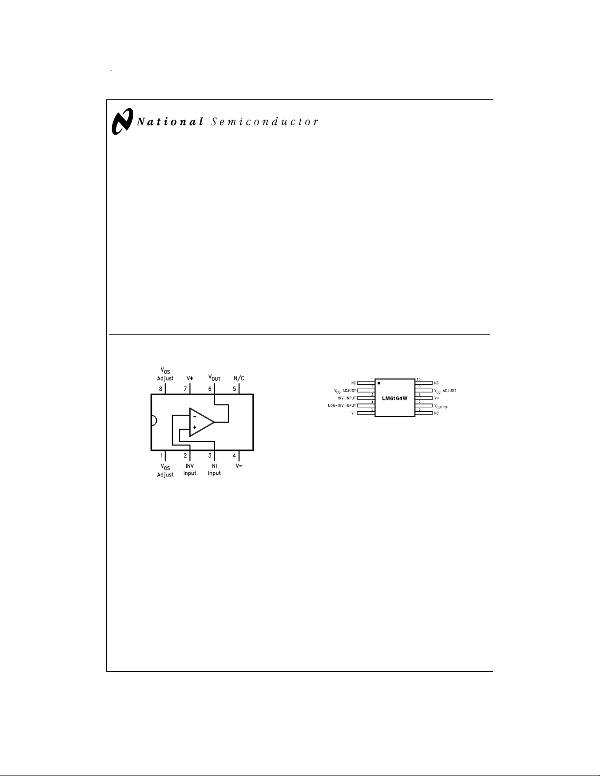
Connection Diagrams
Features
n High slew rate: 300 V/µs
n High GBW product: 175 MHz
n Low supply current: 5 mA
n Fast settling: 100 ns to 0.1
n Low differential gain:
n Low differential phase:
n Wide supply range: 4.75V to 32V
n Stable with unlimited capacitive load
%
<
%
0.1
<
0.1˚
Applications
n Video amplifier
n Wide-bandwidth signal conditioning
n Radar
n Sonar
10-Lead Flatpak
NS Package Number W10A
Top View
DS009153-15
DS009153-8
NS Package Number
J08A, M08A or N08E
VIP™is a trademark of National Semiconductor Corporation.
© 1999 National Semiconductor Corporation DS009153 www.national.com
Page 2
Connection Diagrams (Continued)
Temperature Range Package NSC
Military Industrial Commercial
−55˚C ≤ T
LM6164J/883 8-Pin Ceramic DIP J08A
5962-8962401PA
LM6164WG/883 10-Lead Ceramic SOIC WG10A
5962-8962401XA
LM6164W/883 10-Pin W10A
5962-8962401HA Ceramic Flatpak
≤ +125˚C −25˚C ≤ TA≤ +85˚C 0˚C ≤ TA≤ +70˚C
A
LM6264N LM6364N 8-Pin Molded DIP N08E
LM6364M 8-Pin Molded Surface Mt. M08A
Drawing
www.national.com 2
Page 3
Absolute Maximum Ratings (Note 1)
If Military/Aerospace specified devices are required,
please contact the National Semiconductor Sales Office/
Distributors for availability and specifications.
Supply Voltage (V
Differential Input Voltage
(Note 7)
Common-Mode Input Voltage
(Note 11) (V
Output Short Circuit to Gnd
(Note 2) Continuous
Soldering Information
Dual-In-Line Package (N, J)
Soldering (10 sec.) 260˚C
Small Outline Package (M)
Vapor Phase (60 sec.) 215˚C
Infrared (15 sec.) 220˚C
+−V−
) 36V
+
− 0.7V) to (V−+ 0.7V)
±
See AN-450 “Surface Mounting Methods and Their Effect
on Product Reliability” for other methods of soldering
surface mount devices.
Storage Temperature Range −65˚C to +150˚C
Max Junction Temperature
(Note 3) 150˚C
ESD Tolerance (Notes 7, 8)
8V
Operating Ratings
Temperature Range (Note 3)
LM6164 −55˚C ≤ T
LM6264 −25˚C ≤ T
LM6364 0˚C ≤ T
Supply Voltage Range 4.75V to 32V
Note 1: “Absolute Maximum Ratings” indicate limits beyond which damage
to the device may occur. Operating Ratings indicate conditions for which the
device is functional, but do not guarantee specific performance limits.
±
≤ +125˚C
J
≤ +85˚C
J
≤ +70˚C
J
700V
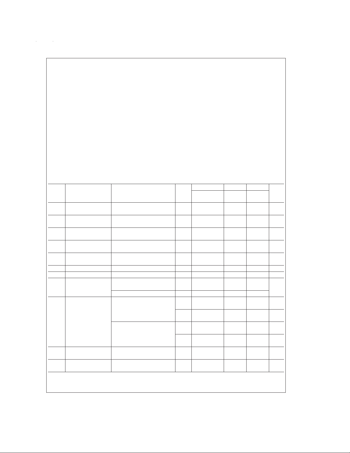
DC Electrical Characteristics
=
The following specifications apply for Supply Voltage
Boldface limits apply for T
=
=
T
A
to T
T
J
MIN
MAX
±
15V, V
; all other limits T
Symbol Parameter Conditions Typ Limit Limit Limit Units
V
V
Input Offset Voltage 2 4 4 9 mV
OS
Input Offset Voltage 6 µV/˚C
OS
Drift Average Drift
I
b
I
OS
I
OS
Input Bias Current 2.5 3 3 5 µA
Input Offset Current 150 350 350 1500 nA
Input Offset Current 0.3 nA/˚C
Drift Average Drift
R
C
A
Input Resistance Differential 100 kΩ
IN
Input Capacitance 3.0 pF
IN
Large Signal V
VOL
OUT
=
±
10V, R
=
2kΩ 2.5 1.8 1.8 1.3 V/mV
L
Voltage Gain (Note 10) 0.9 1.2 1.1 min
=
R
10 kΩ 9
L
=
V
Input Common-Mode Supply
CM
±
15V +14.0 +13.9 +13.9 +13.8 V
Voltage Range +13.8 +13.8 +13.7 min
Supply=+5V 4.0 3.9 3.9 3.8 V
(Note 5) 3.8 3.8 3.7 min
CMRR Common-Mode −10V ≤ V
≤ +10V 105 86 86 80 dB
CM
Rejection Ratio 80 82 78 min
PSRR Power Supply
±
10V ≤ V±≤±16V 96 86 86 80 dB
Rejection Ratio 80 82 78 min
=
≥ 100 kΩ and R
0, R
CM
L
=
=
T
25˚C.
A
J
=
50Ω unless otherwise noted.
S
LM6164 LM6264 LM6364
(Notes 4, 12) (Note 4) (Note 4)
6611max
656max
800 600 1900 max
−13.5 −13.3 −13.3 −13.2 V
−13.1 −13.1 −13.1 min
1.5 1.7 1.7 1.8 V
1.9 1.9 1.9 max
www.national.com3
Page 4
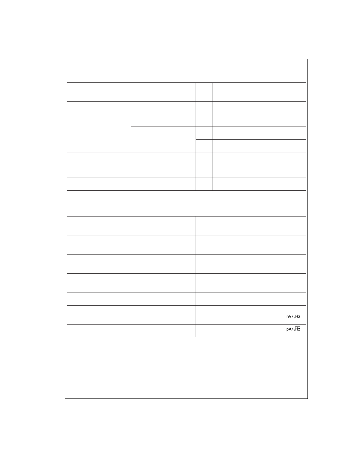
DC Electrical Characteristics (Continued)
=
The following specifications apply for Supply Voltage
Boldface limits apply for T
=
=
T
A
to T
T
J
MIN
MAX
±
15V, V
; all other limits T
Symbol Parameter Conditions Typ Limit Limit Limit Units
V
Output Voltage Supply=+5V +14.2 +13.5 +13.5 +13.4 V
O
Swing and R
=
2kΩ +13.3 +13.3 +13.3 min
L
Supply=+5V 4.2 3.5 3.5 3.4 V
=
and R
2kΩ 3.3 3.3 3.3 min
L
(Note 10) 1.3 1.7 1.7 1.8 V
Output Short Source 65 30 30 30 mA
Circuit Current 20 25 25 min
Sink 65 30 30 30 mA
I
S
Supply Current 5.0 6.5 6.5 6.8 mA
=
≥ 100 kΩ and R
0, R
CM
L
=
=
T
25˚C.
A
J
=
50Ω unless otherwise noted.
S
LM6164 LM6264 LM6364
(Notes 4, 12) (Note 4) (Note 4)
−13.4 −13.0 −13.0 −12.9 V
−12.7 −12.8 −12.8 min
2.0 1.9 1.9 max
20 25 25 min
6.8 6.7 6.9 min
AC Electrical Characteristics
=
The following specifications apply for Supply Voltage
Boldface limits apply for T
=
=
T
A
to T
T
J
MIN
MAX
±
15V, V
; all other limits T
Symbol Parameter Conditions Typ Limit Limit Limit Units
GBW Gain-Bandwidth F=20 MHz 175 140 140 120 MHz
Product 100 120 100
=
±
5V 120
=
+5 (Note 9) 300 200 200 200 V/µs
=
±
5V 200
=
20 V
PP
%
=
=
=
−4, R
2kΩ
L
+5 45 Deg
=
+10
V
=
+10
V
SR Slew Rate A
PBW Power Bandwidth V
T
S
φ
m
A
D
φ
D
e
np-p
Settling Time 10V Step to 0.1
Phase Margin A
Differential Gain NTSC, A
Differential Phase NTSC, A
Input Noise F=10 kHz 8
Supply
V
Supply
OUT
A
V
V
Voltage
i
np-p
Input Noise F=10 kHz 1.5
Current
Note 2: Continuous short-circuit operation at elevated ambient temperature can result in exceeding the maximum allowed junction temperature of 150˚C.
Note 3: The typical junction-to-ambient thermal resistance of the molded plastic DIP (N) is 105˚C/Watt, the molded plastic SO (M) package is 155˚C/Watt, and the
cerdip (J) package is 125˚C/Watt. All numbers apply for packages soldered directly into a printed circuit board.
Note 4: Limits are guaranteed by testing or correlation.
Note 5: For single supply operation, the following conditions apply: V
−
) to realize maximum output swing. This connection will degrade VOS.
Pin4(V
Note 6: C
≤ 5pF.
L
Note 7: Inorder to achieve optimum AC performance, the input stage was designed without protective clamps. Exceeding the maximum differential input voltage results in reverse breakdown of the base-emitter junction of one of the input transistors and probable degradation of the input parameters (especially V
Noise).
Note 8: Theaveragevoltagethattheweakestpincombinations(thoseinvolvingPin2orPin 3) can withstand and still conform to the datasheet limits. The test circuit
used consists of the human body model of 100 pF in series with 1500Ω.
+
=
5V,V
=
≥ 100 kΩ and R
0, R
CM
L
=
=
T
A
25˚C.
J
=
50Ω unless otherwise noted.
S
LM6164 LM6264 LM6364
(Notes 4, 12) (Note 4) (Note 4)
180 180 180
4.5 MHz
100 ns
<
0.1
<
0.1 Deg
−
=
0V,V
=
CM
2.5V,V
=
2.5V.Pin1&Pin8(V
OUT
Adjust) are each connected to
OS
OS,IOS
min
min
%
, and
www.national.com 4
Page 5

AC Electrical Characteristics (Continued)
Note 9: V
Note 10: Voltage Gain is the total output swing (20V) divided by the input signal required to produce that swing.
Note 11: The voltage between V
Note 12: AmilitaryRETS electrical test specification is available on request. At the time of printing, the LM6164J/883 RETS spec complied with the Boldface limits
in this column. The LM6164J/883 may also be procured as Standard Military Drawing
=
4V step. For supply
IN
=
=
±
5V, V
1V step.
IN
+
and either input pin must not exceed 36V.
#
5962-8962401PA.
Typical Performance Characteristics (R
Supply Current vs
Supply Voltage
DS009153-16
Gain-Bandwidth
Product
DS009153-19
Common-Mode
Rejection Ratio
Propagation Delay
Rise and Fall Time
=
L
10 kΩ,T
DS009153-17
DS009153-20
=
25˚C unless otherwise specified)
A
Power Supply
Rejection Ratio
Gain-Bandwidth Product
vs Load Capacitance
DS009153-18
DS009153-21
Slew Rate vs
Load Capacitance
DS009153-22
Overshoot vs
Load Capacitance
DS009153-23
Slew Rate
DS009153-24
www.national.com5
Page 6

Typical Performance Characteristics (R
specified) (Continued)
=
L
10 kΩ,T
=
25˚C unless otherwise
A
Voltage Gain vs
Gain vs Supply Voltage
Load Resistance
DS009153-25
Differential Gain
(Note 13)
Note 13: Differential gain and differential phase measured for four series LM6364 op amps in series with an LM6321 buffer. Error added by LM6321 is negligible.
Test performed using Tektronix Type 520 NTSC test system. Configured with a gain of +5 (each output attenuated by 80%)
DS009153-6
Differential Phase
(Note 13)
DS009153-26
DS009153-7
Step Response; Av=+5
Input (1v /div) Output (5v/div)
TIME (50 ns /div)
www.national.com 6
DS009153-1
Page 7

Typical Performance Characteristics (R
specified) (Continued)
=
L
10 kΩ,T
=
25˚C unless otherwise
A
Input Noise Voltage
Open-Loop
Frequency Response
Common-Mode Input
Saturation Voltage
DS009153-27
DS009153-30
Input Noise Current
Open-Loop
Frequency Response
Output Saturation Voltage
DS009153-28
DS009153-31
Power Bandwidth
DS009153-29
Output Resistance
Open-Loop
DS009153-32
Bias Current vs
Common-Mode Voltage
DS009153-33
DS009153-34
DS009153-35
www.national.com7
Page 8

Simplified Schematic
Applications Tips
The LM6364 hasbeen compensated forgains of 5or greater
(over specified rangesof temperature, powersupply voltage,
and load). Since this compensation involved adding
emitter-degeneration resistors in the op amp’s input stage,
the open-loop gain was reduced as the stability increased.
Gain error due to reduced A
gains; thus, the uncompensated LM6365 is appropriate for
gains of 25 or more. If unity-gain operation is desired, the
LM6361 should be used. The LM6361, LM6364, and
LM6365 have the same high slew rate (typically 300 V/µs),
regardless of their compensation.
The LM6364 is unusually tolerant of capacitive loads. Most
op amps tend to oscillate when their load capacitance is
greater than about 200 pF (in low-gain circuits). However,
load capacitance on the LM6364 effectively increases its
compensation capacitance, thus slowing the op amp’s response and reducing its bandwidth. The compensation isnot
ideal, though, and ringing or oscillation may occur in
low-gain circuits with large capacitiveloads. Toovercompensate the LM6364 for operation at gains less than 5, a series
resistor-capacitor network should be added between the input pins (as shown in the Typical Applications, Noise Gain
Compensation) so that the high-frequency noise gain rises
to at least 5.
is most apparent at high
VOL
DS009153-3
Power supply bypassing will improve the stability and transient response of the LM6364, and is recommended for every design. 0.01 µF to 0.1 µF ceramic capacitors should be
used (from each supply “rail” to ground); if the device is far
away from its power supply source, an additional 2.2 µF to
10 µF (tantalum) may be required for extra noise reduction.
Keep all leads short to reduce stray capacitance andlead inductance, and make sure ground paths are low-impedance,
especially where heavier currents will be flowing. Stray capacitance in the circuit layout can cause signal coupling between adjacent nodes, so that circuit gain unintentionally
varies with frequency.
Breadboarded circuits will work best if they are built using
generic PC boards with a good ground plane. If the op amps
are used with sockets, asopposed to being soldered into the
circuit, the additional input capacitance may degrade circuit
performance.
www.national.com 8
Page 9

Typical Applications
RXCX≥ (2π•25 MHz)
=
5R
X
R
1+RF
(1+R1/R2)
Offset Voltage Adjustment
DS009153-10
−1
Video-Bandwidth Amplifier
DS009153-12
Noise-Gain Compensation for Gains ≤5
DS009153-11
www.national.com9
Page 10

Physical Dimensions inches (millimeters) unless otherwise noted
Ceramic Dual-In-Line Package (J)
Order Number LM6164J/883
NS Package Number J08A
Molded Package SO (M)
Order Number LM6364M
NS Package Number M08A
www.national.com 10
Page 11

Physical Dimensions inches (millimeters) unless otherwise noted (Continued)
Molded Dual-In-Line Package (N)
Order Number LM6264N or LM6364N
NS Package Number N08E
10-Pin Ceramic Flatpak
Order Number LM6164W/883
NS Package Number W10A
www.national.com11
Page 12

Notes
LM6164/LM6264/LM6364 High Speed Operational Amplifier
LIFE SUPPORT POLICY
NATIONAL’S PRODUCTS ARE NOT AUTHORIZED FOR USE AS CRITICAL COMPONENTS IN LIFE SUPPORT
DEVICES OR SYSTEMS WITHOUT THE EXPRESS WRITTEN APPROVAL OF THE PRESIDENT AND GENERAL
COUNSEL OF NATIONAL SEMICONDUCTOR CORPORATION. As used herein:
1. Life support devices or systems are devices or
systems which, (a) are intended for surgical implant
into the body, or (b) support or sustain life, and
whose failure to perform when properly used in
accordance with instructions for use provided in the
labeling, can be reasonably expected to result in a
significant injury to the user.
National Semiconductor
Corporation
Americas
Tel: 1-800-272-9959
Fax: 1-800-737-7018
Email: support@nsc.com
www.national.com
National does not assume any responsibility for use of any circuitry described, no circuit patent licenses are implied and National reserves the right at any time without notice to change said circuitry and specifications.
National Semiconductor
Europe
Fax: +49 (0) 1 80-530 85 86
Email: europe.support@nsc.com
Deutsch Tel: +49 (0) 1 80-530 85 85
English Tel: +49 (0) 1 80-532 78 32
Français Tel: +49 (0) 1 80-532 93 58
Italiano Tel: +49 (0) 1 80-534 16 80
2. A critical component is any component of a life
support device or system whose failure to perform
can be reasonably expected to cause the failure of
the life support device or system, or to affect its
safety or effectiveness.
National Semiconductor
Asia Pacific Customer
Response Group
Tel: 65-2544466
Fax: 65-2504466
Email: sea.support@nsc.com
National Semiconductor
Japan Ltd.
Tel: 81-3-5639-7560
Fax: 81-3-5639-7507
 Loading...