

Page 1
LM6121/LM6221/LM6321
High Speed Buffer
LM6121/LM6221/LM6321 High Speed Buffer
May 1998
General Description
These high speed unity gain buffers slew at 800 V/µs and
have a small signal bandwidth of 50 MHz while driving a 50Ω
load. They can drive
while driving large capacitive loads. The LM6121 family are
monolithic ICs which offer performance similar to the
LH0002 with the additional features of current limit and thermal shutdown.
These buffers are built with National’s VIP
grated PNP) process which provides fast PNP transistors
that are true complements to the already fast NPN devices.
This advanced junction-isolated process delivers high speed
performance without the need for complex and expensive dielectric isolation.
±
300 mA peak and do not oscillate
™
(Vertically Inte-
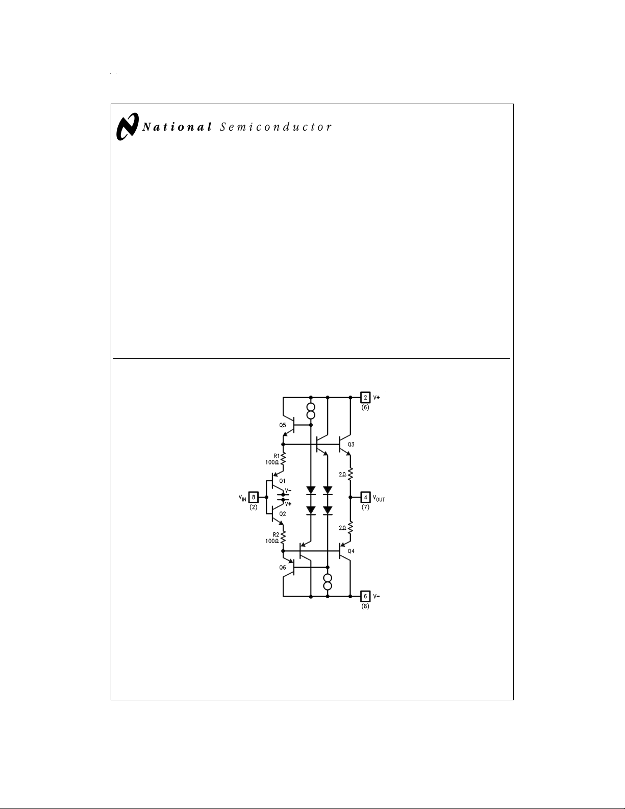
Simplified Schematic
Features
n High slew rate: 800 V/µs
n Wide bandwidth: 50 MHz
n Slew rate and bandwidth 100%tested
n Peak output current:
n High input impedance: 5 MΩ
n LH0002H pin compatible
n No oscillations with capacitive loads
±
n 5V to
n Current and thermal limiting
n Fully specified to drive 50Ω lines
15V operation guaranteed
±
300 mA
Applications
n Line Driving
n Radar
n Sonar
Numbers in ( ) are for 8-pin N DIP.
VIP™is a trademark ofNational Semiconductor Corporation.
© 1999 National Semiconductor Corporation DS009223 www.national.com
DS009223-1
Page 2
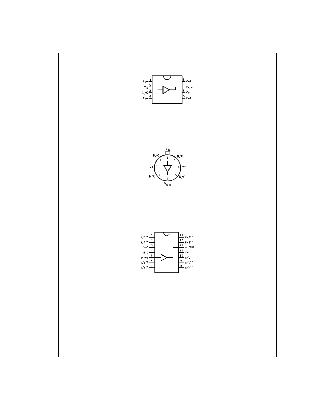
Connection Diagrams
Plastic DIP
*Heat-sinking pins. See Application section on heat sinking requirements.
Order Number LM6221N,
LM6321N or LM6121J/883
See NS Package
Number J08A or N08E
Note: Pin 6 connected to case.
Order Number LM6221H or
See NS Package
DS009223-2
Metal Can
DS009223-3
Top View
LM6121H/883
Number H08C
Plastic SO
*Pin 3 must be connected to the negative supply.
**Heat-sinking pins. See Application section on heat-sinking requirements.
These pins are at V
−
potential.
Order Number LM6321M
See NS Package Number M14A
www.national.com 2
DS009223-7
Page 3
Absolute Maximum Ratings (Note 1)
If Military/Aerospace specified devices are required,
please contact the National Semiconductor Sales Office/
Distributors for availability and specifications.
±
Vsupply
±
2000V
±
18)
±
7V
Supply Voltage 36V (
Input to Output Voltage (Note 2)
Input Voltage
Output Short-Circuit to GND Continuous
(Note 3)
Storage Temperature Range −65˚C to +150˚C
Lead Temperature
(Soldering, 10 seconds) 260˚C
Power Dissipation (Note 10)
ESD Tolerance (Note 8)
Junction Temperature (T
) 150˚C
J(max)
Operating Ratings
Operating Temperature Range
LM6121H/883 −55˚C to +125˚C
LM6221 −40˚C to +85˚C
LM6321 0˚C to +70˚C
Operating Supply Range 4.75 to
Thermal Resistance (θ
H Package 150˚C/W
N Package 47˚C/W
M Package 69˚C/W
Thermal Resistance (θ
), (Note 4)
JA
), H Package 17˚C/W
JC
±
16V
DC Electrical Characteristics
=
The following specifications apply for Supply Voltage
Boldface limits apply for T
=
=
T
A
to T
T
J
MIN
MAX
±
15V, V
; all other limits T
Symbol Parameter Conditions Typ LM6121 LM6221 LM6321 Units
A
A
A
Voltage Gain 1 R
V1
Voltage Gain 2 R
V2
Voltage Gain 3 R
V3
(Note 6) V
V
I
R
C
R
I
I
V
V
V
V
Offset Voltage R
OS
Input Bias Current R
B
Input Resistance R
IN
Input Capacitance 3.5 pF
IN
Output Resistance I
O
Supply Current 1 R
S1
Supply Current 2 R
S2
Output Swing 1 R
O1
Output Swing 2 R
O2
Output Swing 3 R
O3
Output Swing 4 R
O4
=
1kΩ,V
L
=
50Ω,V
L
=
50Ω,V
L
=
2V
IN
=
1kΩ 15 30 30 50 mV
L
=
1kΩ,R
L
=
50Ω 5MΩ
L
=
OUT
=
∞
L
=
∞
L
=
1k 13.5 13.3 13.3 13.2
L
=
100Ω 12.7 11.5 11.5 11
L
=
50Ω 12 11 11 10
L
=
50Ω,V
L
=
±
10V 0.990 0.980 0.980 0.970
IN
=
±
10V 0.900 0.860 0.860 0.850 V/V
IN
+
=
5V 0.840 0.780 0.780 0.750
(1.5 Vpp) 0.750 0.700 0.700
pp
=
10 kΩ 14 45µA
S
±
10 mA 3 5 5 5 Ω
+
=
,V
5V 14 16 16 18
+
=
5V 1.8 1.6 1.6 1.6 V
(Note 6) 1.3 1.4 1.5 Min
±
=
PSSR Power Supply V
±
5V to±15V 70 60 60 60 dB
Rejection Ratio 55 50 50 Min
=
≥ 100 kΩ and R
0, R
CM
L
=
=
T
25˚C.
A
J
=
50Ω unless otherwise noted.
S
Limit Limit Limit
(Notes 5, 9) (Note 5) (Note 5)
0.970 0.950 0.950
0.800 0.820 0.820 Min
50 60 100 Max
777Max
10 10 6 Max
15 18 18 20 mA
20 20 22
18 18 20
13 13 13
10 10 10 Min
999
Max
±
PP
V
www.national.com3
Page 4

AC Electrical Characteristics
=
The following specifications apply for Supply Voltage
Boldface limits apply for T
=
=
T
A
to T
T
J
MIN
MAX
±
15V, V
; all other limits T
Symbol Parameter Conditions Typ LM6121 LM6221 LM6321 Units
SR
SR
Slew Rate 1 V
1
Slew Rate 2 V
2
=
±
IN
=
±
IN
11V, R
11V, R
=
1kΩ 1200 550 550 550 V/µs
L
=
50Ω 800 550 550 550
L
(Note 7)
SR
Slew Rate 3 V
3
BW −3 dB Bandwidth V
t
r,tf
Rise Time R
Fall Time V
t
pd
Propagation R
Delay Time V
O
S
Note 1: Absolute Maximum Ratings indicate limits beyond which damage to the device may occur. DC andAC electrical specifications do not apply when operating
the device beyond its rated operating conditions.
Note 2: During current limit or thermal limit, the input current will increase if the input to output differential voltage exceeds 8V. For input to output differential voltages
in excess of 8V the input current should be limited to
Note 3: The LM6121 series buffers contain current limit and thermal shutdown to protect against fault conditions.
Note 4: The thermal resistance θ
4, 5 and 8) are connected to 2 square inches of 2 oz. copper. When installed in a socket, the thermal resistance θ
sistance θ
connected to 1 square inch of 2 oz. copper.
Note 5: Limits are guaranteed by testing or correlation.
Note 6: The input is biased to 2.5V and V
reduced to 1.5 V
Note 7: Slew rate is measured with a
will be approximately
device heating. For slew rate versus junction temperature see typical performance curves. The input pulse amplitude should be reduced to
at temperature extremes. For accurate measurements, the input slew rate should be at least 1700 V/µs.
Note 8: The test circuit consists of the human body model of 120 pF in series with 1500Ω.
Note 9: For specification limits over the full Military Temperature Range, see RETS6121X.
Note 10: The maximum power dissipation is a function of T
(T
Overshoot R
JA
of the device in the M package is measured when soldered directly to a printed circuit board, and the heat-sinking pins (pins 1, 2, 6, 7, 8, 9, 13, 14) are
JA
.
pp
±
10V.Slew rate is calculated for transitions between±5V levels on both rising and falling edges. Ahigh speed measurement is done to minimize
)/θJA.
J(max)–TA
=
2V
IN
+
=
V
5V (Note 6)
=
±
IN
C
≤ 10 pF Min
L
=
50Ω,C
L
=
100 mV
O
=
50Ω,C
L
=
100 mV
O
=
50Ω,C
L
=
V
100 mV
O
of the device in the N package is measured when soldered directly to a printed circuit board, and the heat-sinking pins (pins 1,
swings Vppabout this value. The input swing is 2 Vppat all temperatures except for the AV3 test at −55˚C where it is
IN
±
11V input pulse and 50Ω source impedance at 25˚C. Since voltage gain is typically 0.9 driving a 50Ω load, the output swing
=
50Ω 50 550 550 550
PP,RL
100 mVPP,R
L
L
L
±
20 mA.
=
L
≤10 pF 7.0 ns
PP
≤10 pF 4.0 ns
PP
≤10 pF 10
PP
, θJA, and TA. The maximum allowable power dissipation at any ambient temperature is P
J(max)
=
≥ 100 kΩ and R
0, R
CM
L
=
=
T
25˚C.
A
J
=
50Ω unless otherwise noted.
S
Limit Limit Limit
(Note 5) (Note 5) (Note 5)
Min
50Ω 50 30 30 30 MHz
%
of the N package is 84˚C/W. The thermal re-
JA
±
10V for measurements
D
=
Typical Performance Characteristics T
Frequency Response
DS009223-11
www.national.com 4
Frequency Response
=
25˚C, unless otherwise specified
J
Slew Rate vs Temperature
DS009223-12
DS009223-13
Page 5

Typical Performance Characteristics T
=
25˚C, unless otherwise specified (Continued)
J
Overshoot vs Capacitive Load
DS009223-14
Supply Current
DS009223-17
Slew Rate
Large Signal Response
=
R
1kΩ
L
−3 dB Bandwidth
Power Bandwidth
DS009223-15
DS009223-18
Large Signal Response
=
R
50Ω
L
Slew Rate
Input Return Gain (S11)
DS009223-16
DS009223-19
Forward Transmission
Gain (S12)
DS009223-20
DS009223-23
Current Limit
DS009223-21
DS009223-24
DS009223-22
www.national.com5
Page 6

Application Hints
POWER SUPPLY DECOUPLING
The method of supply bypassing is not critical for stability of
the LM6121 series buffers. However, their high current output combined with high slew rate can result in significant
voltage transients on the power supply lines if much inductance is present. For example, a slew rate of 900 V/µs into a
50Ω load produces a di/dt of 18 A/µs. Multiplying this by a
wiring inductance of 50 nH (which corresponds to approxi-
1
mately 1
minimize this problem use high quality decoupling very close
to the device. Suggested values are a 0.1 µF ceramic in parallel with one or two 2.2 µF tantalums.A ground plane is recommended.
LOAD IMPEDANCE
The LM6121 is stable to any load when driven by a 50Ω
source. As shown in the
graph, worst case is a purely capacitive load of about
1000 pF. Shunting the load capacitance with a resistor will
reduce overshoot.
SOURCE INDUCTANCE
Like any high frequency buffer, the LM6121 can oscillate at
high values of source inductance. The worst case condition
occurs at a purely capacitive load of 50 pF where up to
100 nH of source inductance can be tolerated. With a 50Ω
load, this goes up to 200 nH. This sensitivity may be reduced
at the expense of a slight reduction in bandwidth by adding a
resistor in series with the buffer input. A100Ω resistor will ensure stability with source inductances up to 400 nH with any
load.
OVERVOLTAGE PROTECTION
The LM6121 may be severely damaged or destroyed if the
Absolute Maximum Rating of 7V between input and output
pins is exceeded.
If the buffer’s input-to-output differential voltage is allowed to
exceed 7V, a base-emitter junction will be in
reverse-breakdown, and will be in series with a
forward-biased base-emitter junction. Referring to the
LM6121 simplified schematic, the transistors involved are
Q1 and Q3 for positive inputs, and Q2 and Q4 for negative
inputs. If any current is allowed to flow through these junctions, localized heating of the reverse-biased junction will occur, potentially causing damage. The effect of the damage is
typically increased offset voltage, increased bias current,
and/or degraded AC performance. Furthermore, this will defeat the short-circuit and over-temperature protection circuitry. Exceeding
stroy the device.
The device is best protected by the insertion of the parallel
combination of a 100 kΩ resistor (R1) and a small capacitor
(C1) in series with the buffer input, and a 100 kΩ resistor
(R2) from input to output of the buffer (see
network normally has no effect on the buffer output. However,if the buffer’scurrent limit or shutdown is activated,and
the output has a ground-referred load of significantly less
⁄2" of 22 gauge wire) result in a 0.9V transient. To
Overshoot vs Capacitive Load
±
7V input with a shorted output will de-
Figure 1
). This
than 100 kΩ, a large input-to-output voltage may be present.
R1 and R2 then form a voltage divider, keeping the
input-output differential below the 7V Maximum Rating for input voltages up to 14V. This protection network should be
sufficient to protect the LM6121 from the output of nearly any
op amp which is operated on supply voltages of
±
15V or
lower.
DS009223-6
FIGURE 1. LM6121 with Overvoltage Protection
Application Hints
HEATSINK REQUIREMENTS
A heatsink may be required with the LM6321 depending on
the maximum power dissipation and maximum ambient temperature of the application. Under all possible operatingconditions, the junction temperature must be within the range
specified under Absolute Maximum Ratings.
To determine if a heatsink is required, the maximum power
dissipated by the buffer, P(max), must be calculated.The formula for calculating the maximum allowable power dissipation in any application is P
simple case of a buffer driving a resistive load asin
the maximum DC power dissipation occurs when the output
is at half the supply. Assuming equal supplies, the formula is
=
P
(2V+)+V+2/2 RL.
I
D
S
The next parameter which must be calculated is the maximum allowable temperature rise, T
by using the formula:
T
(max)=TJ(max) − TA(max)
R
where: T
(max) is the maximum allowable junction tem-
J
perature
T
(max) is the maximum ambient temperature
A
Using the calculated values for T
quired value for junction-to-ambient thermal resistance,
θ
, can now be found:
(J–A)
θ
(J–A)
=
D
FIGURE 2.
=
(max)/P(max)
T
R
(max)−TA)/θJA. For the
(T
J
DS009223-8
(max). This is calculated
R
(max) and P(max), the re-
R
Figure 2
,
www.national.com 6
Page 7

Application Hints (Continued)
The heatsink for the LM6321 is made using the PC board
copper.The heat is conducted from the die, through the lead
frame (inside the part), and out the pins which are soldered
to the PC board. The pins used for heat conduction are:
TABLE 1.
Part Package Pins
LM6321N 8-Pin DIP 1, 4, 5, 8
LM6321M 14-Pin SO 1, 2, 3, 6, 7,
8, 9, 13, 14
Figure 3
shows copper patterns which may be used to dissi-
pate heat from the LM6321.
8-Pin DIP
DS009223-9
14-Pin SO
*For best results, use L=2H
DS009223-10
FIGURE 3. Copper Heatsink Patterns
TABLE 2.
Package L (in.) H (in.) θ
J–A
8-Pin DIP 2 0.5 47
14-Pin SO 1 0.5 69
21 57
Table 2
shows some values of junction-to-ambient thermal
resistance (θ
) for values of L and W for 2 oz. copper:
J–A
(˚C/W)
www.national.com7
Page 8

Physical Dimensions inches (millimeters) unless otherwise noted
Order Number LM6221H or LM6121H/883
Metal Can Package (H)
NS Package Number H08C
8-Pin Ceramic Dual-In-Line Package (J)
Order Number LM6121J/883
NS Package Number J08A
www.national.com 8
Page 9

Physical Dimensions inches (millimeters) unless otherwise noted (Continued)
14-Pin Small Outline Package (M)
Order Number LM6321M
NS Package Number M14A
Molded Dual-In-Line Package (N)
Order Number LM6221N or LM6321N
NS Package Number N08E
www.national.com9
Page 10

LM6121/LM6221/LM6321 High Speed Buffer
Notes
LIFE SUPPORT POLICY
NATIONAL’S PRODUCTS ARE NOT AUTHORIZED FOR USE AS CRITICAL COMPONENTS IN LIFE SUPPORT
DEVICES OR SYSTEMS WITHOUT THE EXPRESS WRITTEN APPROVAL OF THE PRESIDENT OF NATIONAL
SEMICONDUCTOR CORPORATION. As used herein:
1. Life support devices or systems are devices or
systems which, (a) are intended for surgical implant
into the body, or (b) support or sustain life, and
whose failure to perform when properly used in
accordance with instructions for use provided in the
2. A critical component is any component of a life
support device or system whose failure to perform
can be reasonably expected to cause the failure of
the life support device or system, or to affect its
safety or effectiveness.
labeling, can be reasonably expected to result in a
significant injury to the user.
National Semiconductor
Corporation
Americas
Tel: 1-800-272-9959
Fax: 1-800-737-7018
Email: support@nsc.com
www.national.com
National does not assume any responsibility for use of any circuitry described, no circuit patent licenses are implied and National reserves the right at any time without notice to change said circuitry and specifications.
National Semiconductor
Europe
Fax: +49 (0) 1 80-530 85 86
Email: europe.support@nsc.com
Deutsch Tel: +49 (0) 1 80-530 85 85
English Tel: +49 (0) 1 80-532 78 32
Français Tel: +49 (0) 1 80-532 93 58
Italiano Tel: +49 (0) 1 80-534 16 80
National Semiconductor
Asia Pacific Customer
Response Group
Tel: 65-2544466
Fax: 65-2504466
Email: sea.support@nsc.com
National Semiconductor
Japan Ltd.
Tel: 81-3-5639-7560
Fax: 81-3-5639-7507
 Loading...