

Page 1
LM6182
Dual 100 mA Output, 100 MHz Current Feedback
Amplifier
General Description
The LM6182 dual current feedback amplifier offers an unparalleled combination of bandwidth, slew-rate, and output current. Each amplifier can directly drive a 2V signal into a 50Ω
or 75Ω back-terminated coax cable system over the full industrial temperature range. This represents a radical enhancement in output drive capability for a dual 8-pin
high-speed amplifier making it ideal for video applications.
Built on National’s advanced high-speed VIP II
™
(Vertically
Integrated PNP) process, the LM6182 employs
current-feedback providing bandwidth that does not vary
dramatically with gain; 100 MHz at Av=−1, 60 MHz at Av
=
−10. With a slew rate of 2000 V/µsec, 2nd harmonic distortion of −50 dBc at 10 MHz and settling time of 50 ns (0.1%),
the two independent amplifiers of the LM6182 offer performance that is ideal for data acquisition, high-speed ATE,and
precision pulse amplifier applications.
See the LM6181 data sheet for a single amplifier with these
same features.
Features
(Typical unless otherwise noted)
n Slew Rate: 2000 V/µs
n Closed Loop Bandwidth: 100 MHz
n Settling Time (0.1%): 50 ns
n Low Differential Gain and Phase Error: 0.05%, 0.04˚
R
L
=
150Ω
n Low Offset Voltage: 2 mV
n High Output Drive:
±
10V into 150Ω
n Characterized for Supply Ranges:
±
5V and±15V
n Improved Performance over OP260 and LT1229
Applications
n Coax Cable Driver
n Professional Studio Video Equipment
n Flash ADC Buffer
n PC and Workstation Video Boards
n Facsimile and Imaging Systems
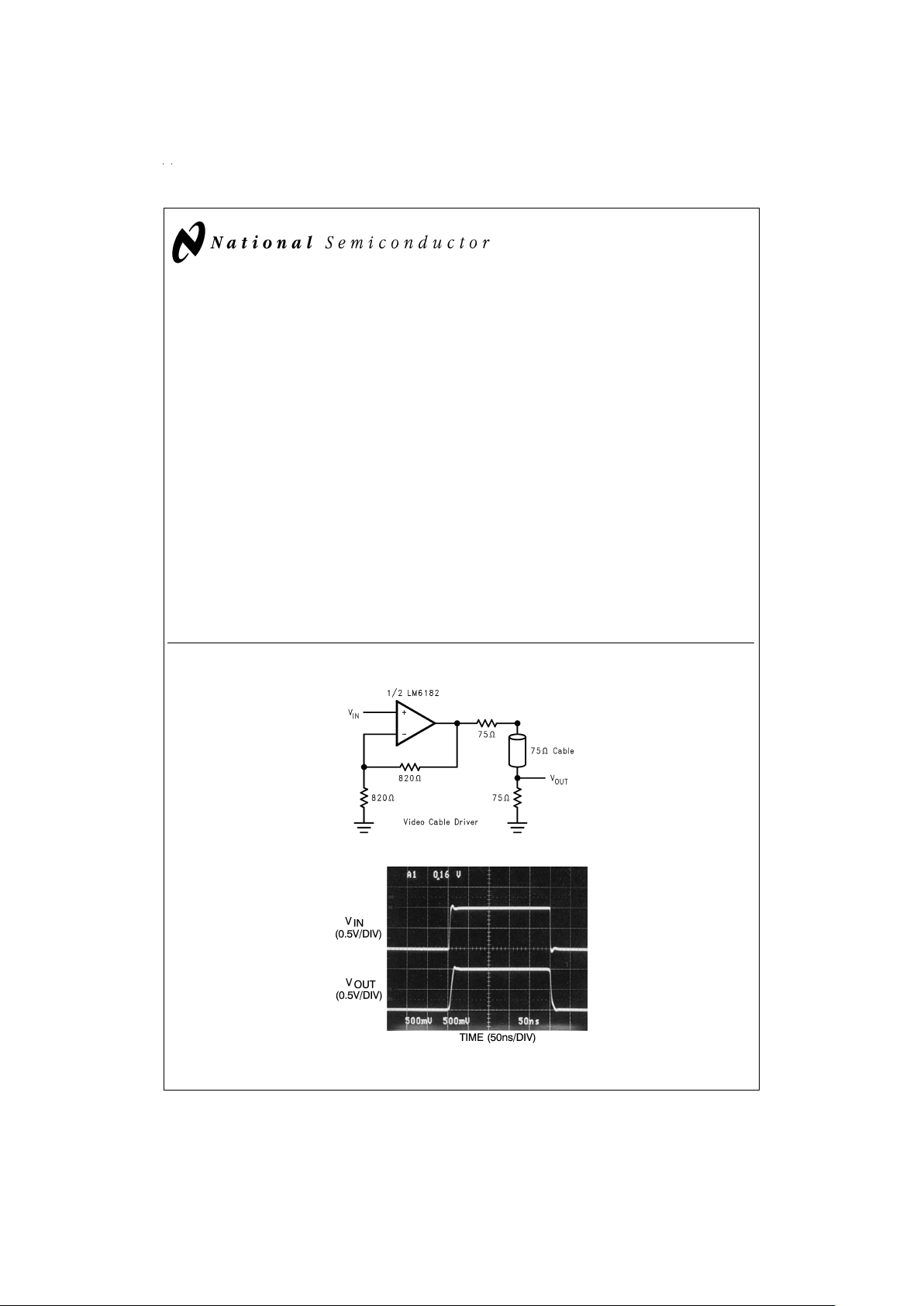
Typical Application
VIP II™is a trademark ofNational Semiconductor Corporation.
DS011926-1
DS011926-2
April 1994
LM6182 Dual 100 mA Output, 100 MHz Current Feedback Amplifier
© 1999 National Semiconductor Corporation DS011926 www.national.com
Page 2
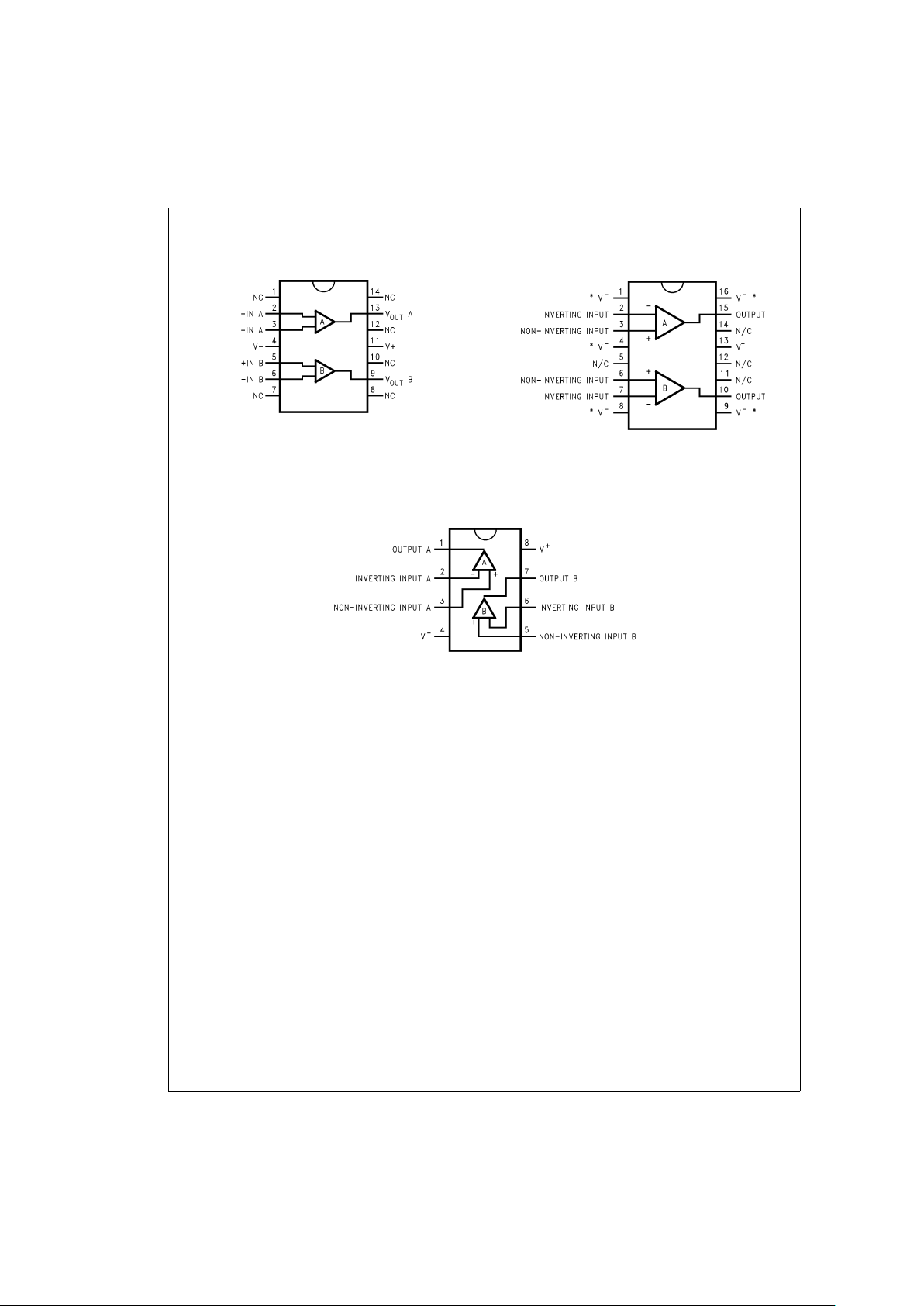
Connection Diagrams
Dual-In-Line Package (J)
DS011926-51
Order Number LM6182AMJ/883
See NS Package Number J14A
Small Outline Package (M)
DS011926-4
*
Heat Sinking Pins (Note 3)
Order Number LM6182IM or LM6182AIM
See NS Package Number M16A
Dual-In-Line Package (N)
DS011926-3
Order Number LM6182IN, LM6182AIN or LM6182AMN
See NS Package Number N08E
www.national.com 2
Page 3
Absolute Maximum Ratings (Note 1)
If Military/Aerospace specified devices are required,
please contact the National Semiconductor Sales Office/
Distributors for availability and specifications.
Supply Voltage
±
18V
Differential Input Voltage
±
6V
Input Voltage
±
Supply Voltage
Inverting Input Current 15 mA
Output Short Circuit (Note 4)
Soldering Information
Dual-In-Line Package (N)
Soldering (10s) 260˚C
Small Outline Package (M)
Vapor Phase (60s) 215˚C
Infrared (15s) 220˚C
Storage Temperature Range −65˚C ≤ T
J
≤ +150˚C
Junction Temperature 150˚C
ESD Rating (Note 2)
±
2000V
Operating Ratings
Supply Voltage Range 7V to 32V
Junction Temperature Range (Note 3)
LM6182AM −55˚C ≤ T
J
≤ +125˚C
LM6182AI, LM6182I −40˚C ≤ T
J
≤ +85˚C
±
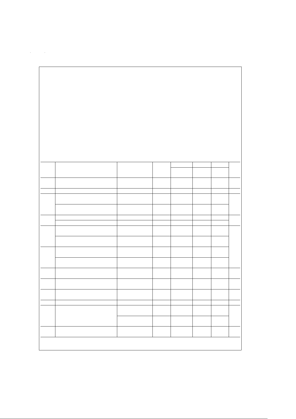
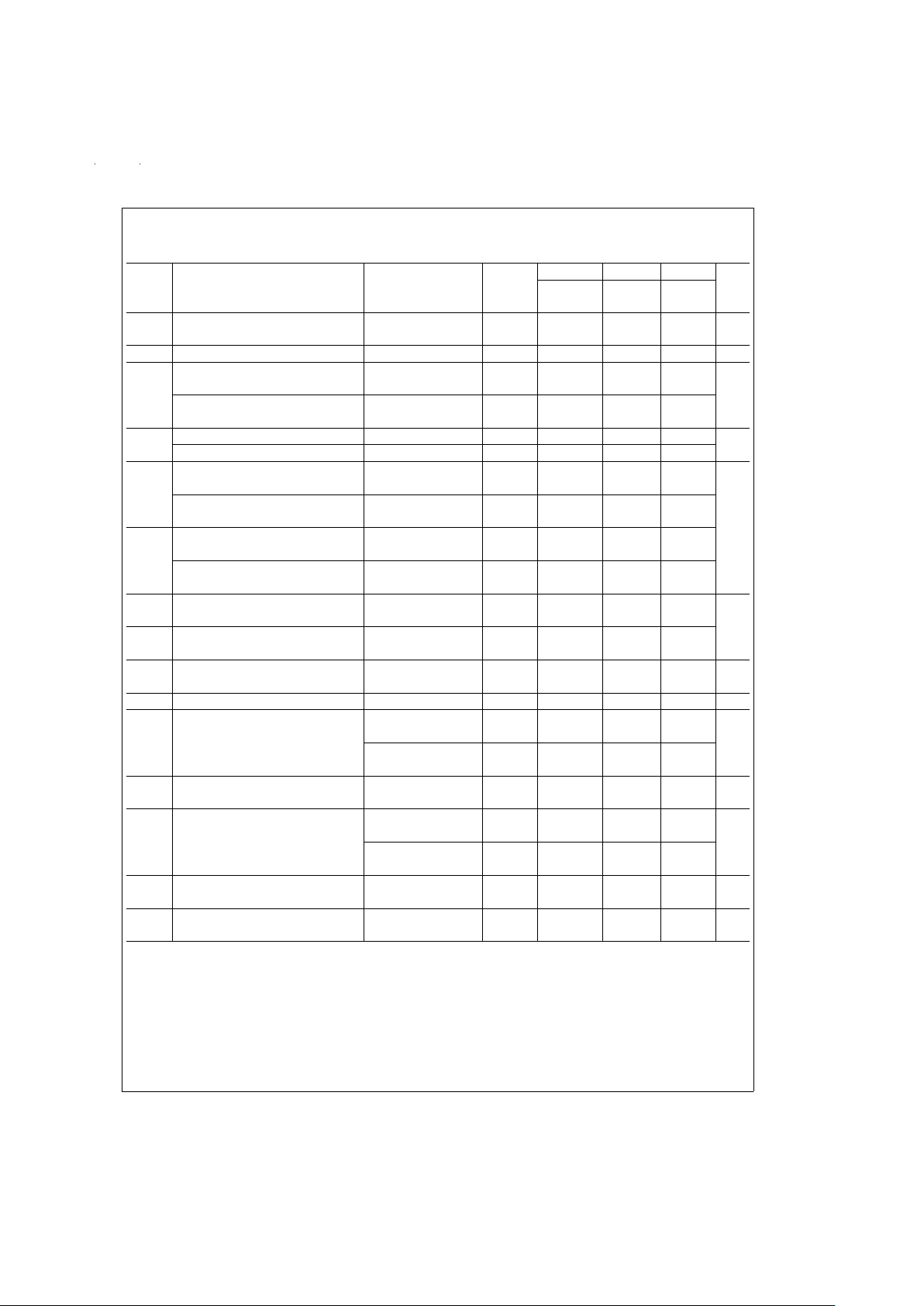
15V DC Electrical Characteristics
The following specifications apply for supply voltage
=
±
15V, Vcm=V
O
=
0V, R
f
=
820Ω, and R
L
=
1kΩunless otherwise
noted. Boldface limits apply at the temperature extremes; all other limits T
J
=
25˚C.
Symbol Parameter Conditions Typical
(Note 5)
LM6182AM LM6182AI LM6182I Units
Limit Limit Limit
(Note 6) (Note 6) (Note 6)
V
OS
Input Offset Voltage 2.0 3.0 3.0 5.0 mV
4.0 3.5 5.5 max
TCV
OS
Input Offset Voltage Drift 5.0 µV/˚C
I
B
Inverting Input Bias Current 2.0 5.0 5.0 10.0 µA
max
12.0 12.0 17.0
Non-Inverting Input Bias Current 0.75 2.0 2.0 3.0
4.0 4.0 5.0
TCI
B
Inverting Input Bias Current Drift 30 nA/˚C
Non-Inverting Input Bias Current Drift 10
I
B
Inverting Input Bias Current
±
4.5V ≤ VS≤±16V 0.1 0.5 0.5 0.75 µA/V
max
PSR Power Supply Rejection 3.0 3.0 4.5
Non-Inverting Input Bias Current
±
4.5V ≤ VS≤±16V 0.05 0.5 0.5 0.5
Power Supply Rejection 1.5 1.5 3.0
I
B
Inverting Input Bias Current −10V ≤ VCM≤ +10V 0.15 0.5 0.5 0.75
CMR Common Mode Rejection 1.0 1.0 1.5
Non-Inverting Input Bias Current −10V ≤ V
CM
≤ +10V 0.1 0.5 0.5 0.5
Common Mode Rejection 1.0 1.0 1.5
CMRR Common Mode Rejection Ratio −10V ≤ V
CM
≤ +10V 60 50 50 50 dB
47 47 47 min
PSRR Power Supply Rejection Ratio
±
4.5V ≤ VS≤±16V 80 70 70 70 dB
67 67 65 min
R
O
Output Resistance A
V
=
−1 0.2 Ω
f=300 kHz
R
IN
Non-Inverting Input Resistance 10 MΩ
V
O
Output Voltage Swing R
L
=
1kΩ 12 11 11 11 V
min
10 10 10
R
L
=
150Ω 11 9.5 9.5 9.5
5.6 6.0 6.0
I
SC
Output Short Circuit Current 100 70 70 70 mA
37.5 40 40 min
www.national.com3
Page 4
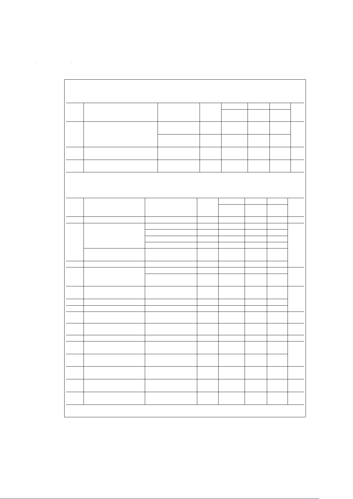
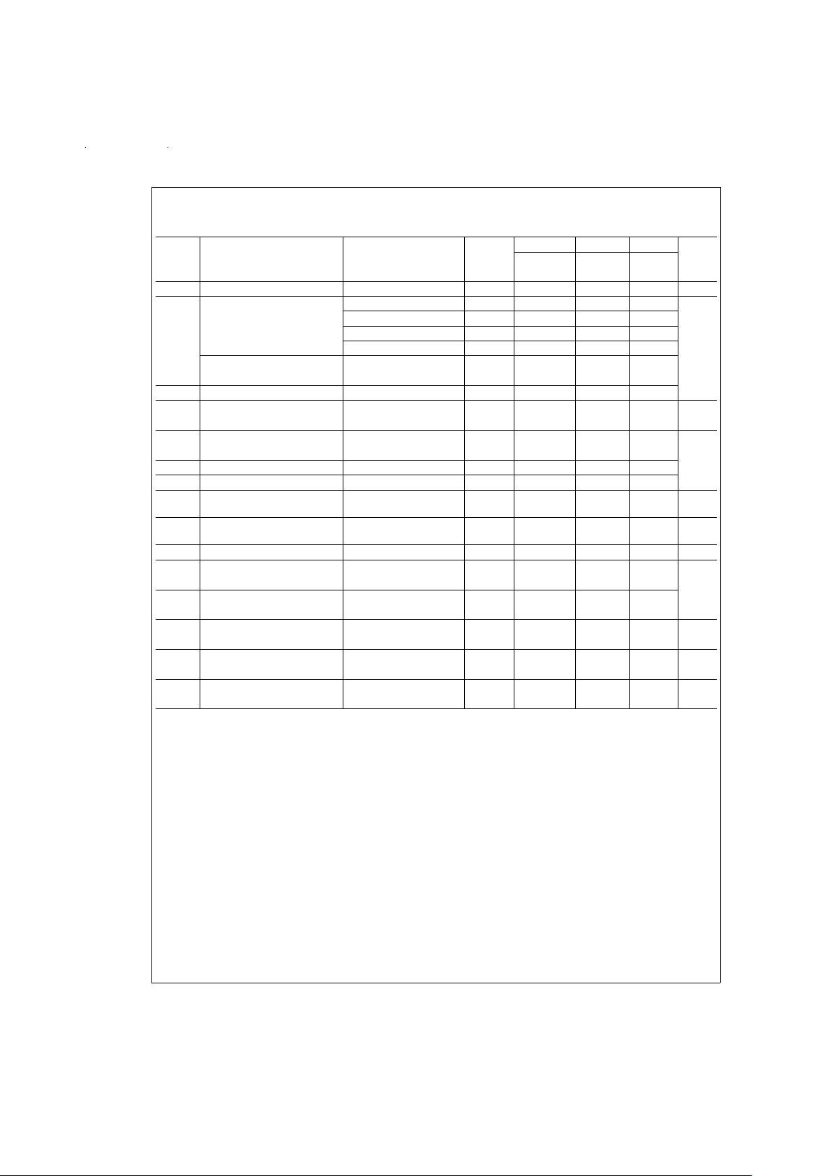
±
15V DC Electrical Characteristics (Continued)
The following specifications apply for supply voltage
=
±
15V, Vcm=V
O
=
0V, R
f
=
820Ω, and R
L
=
1kΩunless otherwise
noted. Boldface limits apply at the temperature extremes; all other limits T
J
=
25˚C.
Symbol Parameter Conditions Typical
(Note 5)
LM6182AM LM6182AI LM6182I Units
Limit Limit Limit
(Note 6) (Note 6) (Note 6)
Z
T
Transimpedance R
L
=
1kΩ 1.8 1.0 1.0 0.8 MΩ
min
0.4 0.5 0.4
R
L
=
150Ω 1.4 0.8 0.8 0.7
0.3 0.35 0.3
I
S
Supply Current No Load, V
IN
=
0V 15 20 20 20 mA
Both Amplifiers 22 22 22 max
V
CM
Input Common Mode Voltage Range V+−1.7V V
V
−
+1.7V
±
15V AC Electrical Characteristics
The following specifications apply for supply voltage
=
±
15V, Vcm=V
O
=
0V, R
f
=
820Ω, and R
L
=
1kΩunless otherwise
noted. Boldface limits apply at the temperature extremes; all other limits T
J
=
25˚C.
Symbol Parameter Conditions Typical
(Note 5)
LM6182AM LM6182AI LM6182I Units
Limit Limit Limit
(Note 6) (Note 6) (Note 6)
Xt Crosstalk Rejection (Note 7) 93 dB
BW Closed Loop Bandwidth −3 dB A
V
=
+2 100 MHz
A
V
=
+10 75
A
V
=
−1 100
A
V
=
−10 60
Closed Loop Bandwidth A
V
=
+2, R
L
=
150Ω 35
0.1 dB Flat, R
SOURCE
=
200Ω
PBW Power Bandwidth A
V
=
−1, V
O
=
5V
PP
60
SR Slew Rate Overdriven 2000 V/µs
min
A
V
=
−1, V
O
=
±
10V 1400 1000 1000 1000
R
L
=
150Ω, (Note 8)
t
s
Settling Time (0.1%)A
V
=
−1, V
O
=
±
5V 50 ns
R
L
=
150Ω
t
r,tf
Rise and Fall Time V
O
=
1V
PP
5
t
p
Propagation Delay Time V
O
=
1V
PP
6
in(+) Non-Inverting Input Noise
Current Density
f=1 kHz 3 pA/
√
Hz
in(−) Inverting Input Noise
Current Density
f=1 kHz 16 pA/
√
Hz
e
n
Input Noise Voltage Density f=1 kHz 4 nV/√Hz
Second Harmonic Distortion V
O
=
2V
PP
,f=10 MHz -50 dBc
A
V
=
+2
Third Harmonic Distortion V
O
=
2V
PP
,f=10 MHz -55
A
V
=
+2
Differential Gain R
L
=
150Ω 0.05
%
A
V
=
+2, NTSC
Differential Phase R
L
=
150Ω 0.04 Deg
A
V
=
+2, NTSC
THD Total Harmonic Distortion V
O
=
2V
PP,AV
=
+2, 0.58
%
f=10 MHz, R
L
=
150Ω
www.national.com 4
Page 5
±
5V DC Electrical Characteristics
The following specifications apply for supply voltage
=
±
5V, Vcm=V
O
=
0V, R
f
=
820Ω, and R
L
=
1kΩunless otherwise
noted. Boldface limits apply at the temperature extremes; all other limits T
J
=
25˚C.
Symbol Parameter Conditions Typical
(Note 5)
LM6182AM LM6182AI LM6182I Units
Limit Limit Limit
(Note 6) (Note 6) (Note 6)
V
OS
Input Offset Voltage 1.0 2.0 2.0 3.0 mV
3.0 2.5 3.5 max
TCV
OS
Input Offset Voltage Drift 2.5 µV/˚C
I
B
Inverting Input Bias Current 5.0 10 10 17.5 µA
max
22 22 27.0
Non-Inverting Input Bias Current 0.25 1.5 1.5 3.0
3.0 3.0 5.0
TCI
B
Inverting Input Bias Current Drift 50 nA/˚C
Non-Inverting Input Bias Current Drift 3.0
I
B
Inverting Input Bias Current
±
4V ≤ VS≤±6V 0.3 0.5 0.5 0.75 µA/V
max
PSR Power Supply Rejection 1.0 1.0 1.5
Non-Inverting Input Bias Current
±
4V ≤ VS≤±6V 0.05 0.5 0.5 0.5
Power Supply Rejection 1.0 1.0 1.5
I
B
Inverting Input Bias Current −2.5V ≤ VCM≤ +2.5V 0.3 0.5 0.5 1.0
CMR Common Mode Rejection 1.0 1.0 1.5
Non-Inverting Input Bias Current −2.5V ≤ V
CM
≤ +2.5V 0.12 0.5 0.5 0.5
Common Mode Rejection 1.0 1.0 1.5
CMRR Common Mode Rejection Ratio −2.5V ≤ V
CM
≤ +2.5V 57 50 50 50 dB
min
47 47 47
PSRR Power Supply Rejection Ratio
±
4V ≤ VS≤±6V 80 70 70 64
67 67 60
R
O
Output Resistance A
V
=
−1 0.25 Ω
f=300 kHz
R
IN
Non-Inverting Input Resistance 8 MΩ
V
O
Output Voltage Swing R
L
=
1kΩ 2.6 2.25 2.25 2.25 V
min
2.0 2.0 2.0
R
L
=
150Ω 2.2 2.0 2.0 2.0
1.8 1.8 1.8
I
SC
Output Short Circuit Current 100 65 65 65 mA
35 40 40 min
Z
T
Transimpedance R
L
=
1kΩ 1.4 0.75 0.75 0.6 MΩ
min
0.3 0.35 0.3
R
L
=
150Ω 1.0 0.5 0.5 0.4
0.2 0.25 0.2
I
S
Supply Current No Load, V
IN
=
0V 13 17 17 17 mA
Both Amplifiers 18.5 18.5 18.5 max
V
CM
Input Common Mode Voltage Range V+−1.7V V
V
−
+1.7V
www.national.com5
Page 6
±
5V AC Electrical Characteristics
The following specifications apply for supply voltage
=
±
5V, Vcm=V
O
=
0V, R
f
=
820Ω, and R
L
=
1kΩunless otherwise
noted. Boldface limits apply at the temperature extremes; all other limits T
J
=
25˚C.
Symbol Parameter Conditions Typical
(Note 5)
LM6182AM LM6182AI LM6182I Units
Limit Limit Limit
(Note 6) (Note 6) (Note 6)
Xt Crosstalk Rejection (Note 7) 92 dB
BW Closed Loop Bandwidth −3 dB A
V
=
+2 50 MHz
A
V
=
+10 40
A
V
=
−1 55
A
V
=
−10 35
Closed Loop Bandwidth A
V
=
+2, R
L
=
150Ω 15
0.1 dB Flat, R
SOURCE
=
200Ω
PBW Power Bandwidth A
V
=
−1, V
O
=
4V
PP
40
SR Slew Rate A
V
=
−1, V
O
=
±
2V 500 375 375 375 V/µs
R
L
=
150Ω, (Note 8) min
t
s
Settling Time (0.1%)A
V
=
−1, V
O
=
±
2V 50 ns
R
L
=
150Ω
t
r,tf
Rise and Fall Time V
O
=
1V
PP
8.5
t
p
Propagation Delay Time V
O
=
1V
PP
8
in(+) Non-Inverting Input Noise
Current Density
f=1 kHz 3 pA/
√
Hz
in(−) Inverting Input Noise
Current Density
f=1 kHz 16 pA/
√
Hz
e
n
Input Noise Voltage Density f=1 kHz 4 nV/√Hz
Second Harmonic Distortion V
O
=
2V
PP
,f=10 MHz -45 dBc
A
V
=
+2
Third Harmonic Distortion V
O
=
2V
PP
,f=10 MHz -55
A
V
=
+2
Differential Gain R
L
=
150Ω 0.06
%
A
V
=
+2, NTSC
Differential Phase R
L
=
150Ω 0.16 Deg
A
V
=
+2, NTSC
THD Total Harmonic Distortion V
O
=
2V
PP,AV
=
+2, 0.36
%
f=5 MHz, R
L
=
150Ω
Note 1: Absolute Maximum Ratings indicate limits beyond which damage to the device may occur. Operating ratings indicate conditions for which the device is intended to be functional, but device parameter specifications may not be guaranteed under these conditions. For guaranteed specifications and test conditions, see
the Electrical Characteristics.
Note 2: Human body model 100 pF and 1.5 kΩ.
Note 3: The typical junction-to-ambient thermal resistance of the molded plastic DIP(N) soldered directly into a PC board is 95˚C/W. The junction-to-ambient thermal
resistance of the S.O. surface mount (M) package mounted flush to the PC board is 70˚C/W when pins 1,4,8,9 and 16 are soldered to a total of 2 in
2
1 oz copper
trace. The S.O. (M) package must have pin 4 and at least one of pins 1,8,9, or 16 connected to V− for proper operation.
Note 4: Continuous short circuit operation at elevated ambient temperature can result in exceeding the maximum allowable junction temperature of 150˚C. Each am-
plifier of the LM6182 is short circuit current limited to 100 mA typical.
Note 5: Typical values represent the most likely parametric norm.
Note 6: All limits are guaranteed at room temperature (standard type face) or at operating temperature extremes (boldface type).
Note 7: Each amp excited in turn with 100 kHz to produce Vo=2 Vpp. Results are input referred.
Note 8: Measured from +25%to +75%of output waveform.
Note 9: Also available per the Standard Military Drawing, 5962-9460301MCA.
Note 10: For guaranteed military specifications see military datasheet MNLM6182AM-X.
www.national.com 6
Page 7
±
5V AC Electrical Characteristics (Continued)
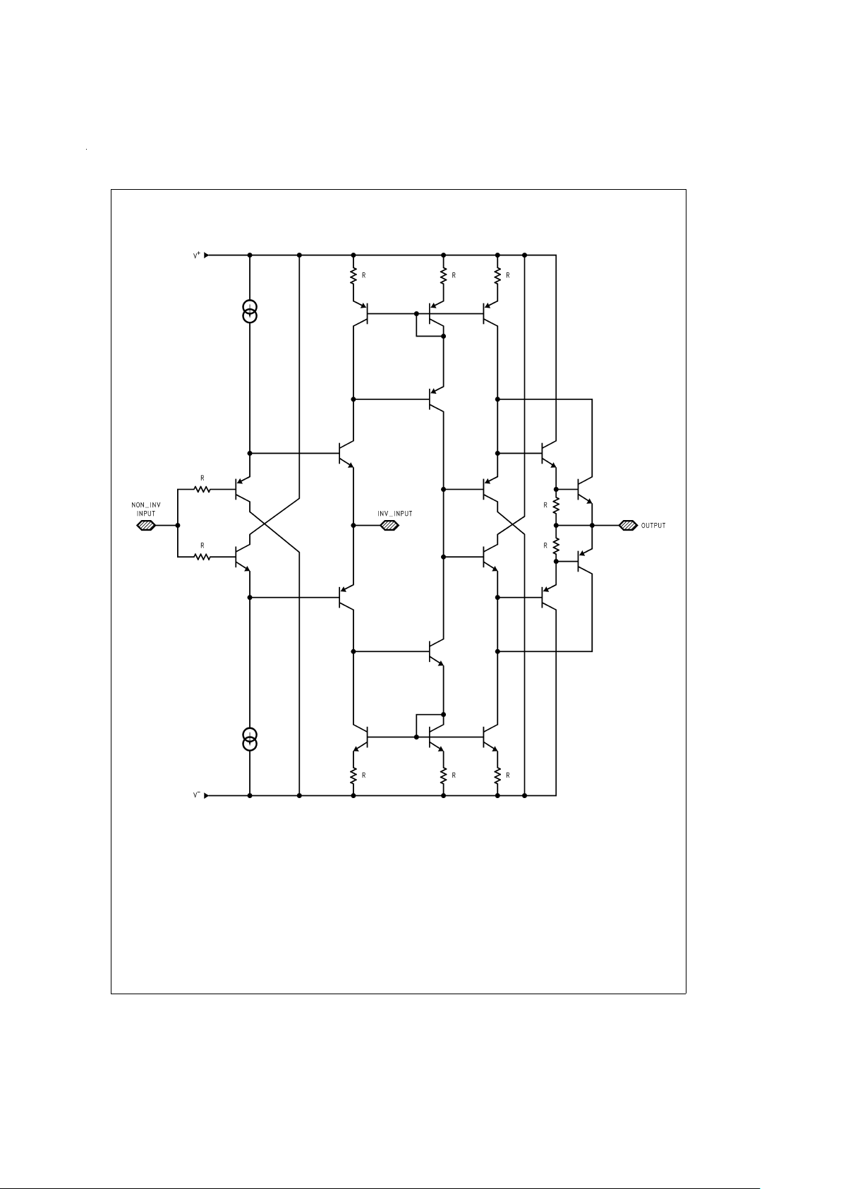
Simplified Schematic 1/2 LM6182
DS011926-6
www.national.com7
Page 8
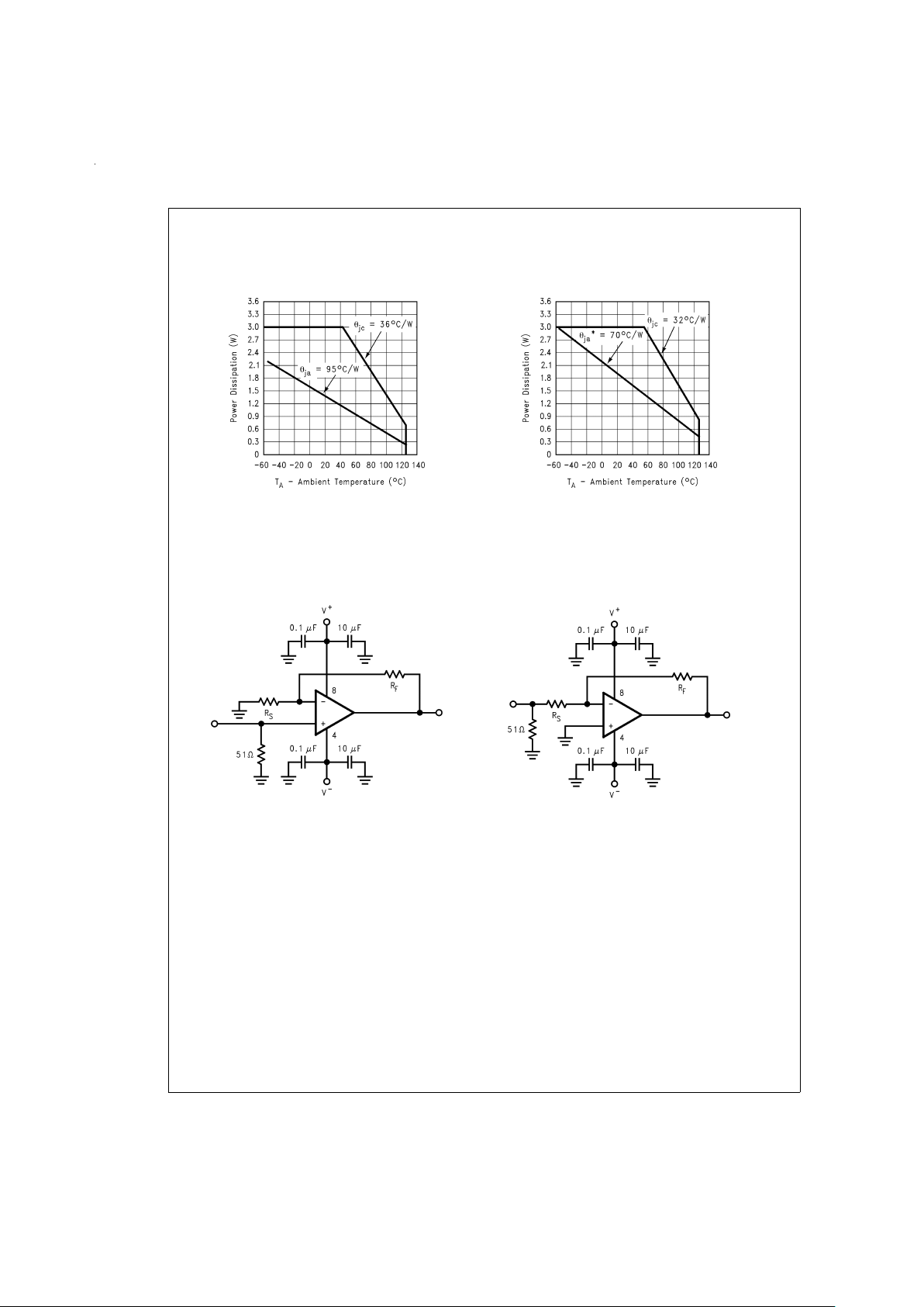
Typical Performance Characteristics
MAXIMUM POWER DERATING CURVES
TYPICAL PERFORMANCE TEST CIRCUITS
N-Package
DS011926-7
M-Package
DS011926-8
*
θ
ja
=
Thermal Resistance with 2 square inches of 1 ounce copper tied to
pins 1, 8, 9 and 16
Non-Inverting:
Small Signal Pulse Response,
Slew Rate, −3 dB Bandwidth
DS011926-9
Inverting:
Small Signal Pulse Response,
Slew Rate, −3 dB Bandwidth
DS011926-10
www.national.com 8
Page 9

TYPICAL PERFORMANCE TEST CIRCUITS (Continued)
Amplifier-to-Amplifier Isolation
DS011926-11
Input Voltage Noise
DS011926-12
CMRR
DS011926-13
PSRR (VS+)
DS011926-14
www.national.com9
Page 10

Typical Performance Characteristics V
S
=
±
15V and T
A
=
25˚C unless otherwise noted.
Inverting Gain
Frequency Response
V
S
=
±
15V, A
V
=
−1, R
f
=
820Ω
DS011926-52
Inverting Gain
Frequency Response
V
S
=
±
5V, A
V
=
−1, R
f
=
820Ω
DS011926-53
Non-Inverting Gain
Frequency Response
V
S
=
±
15V, A
V
=
+2, R
f
=
820Ω
DS011926-54
Non-Inverting Gain
Frequency Response
V
S
=
±
5V, A
V
=
+2, R
f
=
820Ω
DS011926-55
−3 dB Bandwidth vs
R
f
and Rs,A
V
=
+2
DS011926-56
Inverting Gain vs
−3 dB Bandwidth
R
f
=
820Ω
DS011926-57
Non-Inverting Gain vs
−3 dB Bandwidth
R
f
=
820Ω
DS011926-58
−3 dB Bandwidth vs
Supply Voltage
A
V
=
−1
DS011926-59
Transimpedance vs
Frequency
R
L
=
1kΩ
DS011926-60
www.national.com 10
Page 11

Typical Performance Characteristics V
S
=
±
15V and T
A
=
25˚C unless otherwise
noted. (Continued)
Transimpedance vs
Frequency
R
L
=
150Ω
DS011926-61
Settling Response
V
S
=
±
15V, R
L
=
150Ω
A
V
=
−1, V
O
=
±
5V
DS011926-62
Settling Response
V
S
=
±
5V, R
L
=
150Ω
A
V
=
−1, V
O
=
±
2V
DS011926-63
Long Term Settling Time
Response V
S
=
±
15V,
R
L
=
150Ω,A
V
=
−1, V
O
=
±
5V
DS011926-64
Suggested Rfand
R
s
for CL,A
V
=
−1
DS011926-65
Suggested Rfand
R
s
for CL,A
V
=
+2
DS011926-66
Output Impedance vs Frequency
A
V
=
−1, R
L
=
820Ω
DS011926-67
PSRR (VS+)vs
Frequency, A
V
=
2,
R
f
=
R
s
=
820Ω
DS011926-68
www.national.com11
Page 12

Typical Performance Characteristics V
S
=
±
15V and T
A
=
25˚C unless otherwise
noted. (Continued)
PSRR (V
S−
)vs
Frequency, A
V
=
2,
R
f
=
R
s
=
820Ω
DS011926-69
CMRR vs Frequency
R
f
=
R
s
=
820Ω
DS011926-70
Input Voltage Noise
vs Frequency
DS011926-71
Input Current Noise
vs Frequency
DS011926-72
Slew Rate vs Temperature
A
V
=
−1, R
L
=
150Ω
DS011926-73
Slew Rate vs Supply Voltage
A
V
=
−1, R
L
=
150Ω
DS011926-74
Distortion vs Frequency
V
S
=
±
15V, A
V
=
+2,
R
L
=
150Ω,V
O
=
2Vp-p
DS011926-75
Distortion vs Frequency
V
S
=
±
15V, A
V
=
−1,
R
L
=
150Ω,V
O
=
2Vp-p
DS011926-76
Distortion vs Frequency
V
S
=
±
5V, A
V
=
+2,
R
L
=
150Ω,V
O
=
2Vp-p
DS011926-77
www.national.com 12
Page 13

Typical Performance Characteristics V
S
=
±
15V and T
A
=
25˚C unless otherwise
noted. (Continued)
Distortion vs Frequency
V
S
=
±
5V, A
V
=
−1,
R
L
=
150Ω,V
O
=
2Vp-p
DS011926-78
Crosstalk Rejection vs
Frequency
DS011926-79
Maximum Output Voltage
Swing vs Frequency
(THD ≤ 1%)
DS011926-80
−3 dB Bandwidth
vs Temperature, A
V
=
−1
DS011926-81
−3 dB Bandwidth
vs Temperature, A
V
=
+2
DS011926-82
Small Signal Pulse Response
vs Temperature, A
V
=
−1,
V
S
=
±
15V, R
L
=
1kΩ
DS011926-83
Small Signal Pulse Response
vs Temperature, A
V
=
−1,
V
S
=
±
15V, R
L
=
150Ω
DS011926-84
Small Signal Pulse Response
vs Temperature, A
V
=
+2,
V
S
=
±
15V, R
L
=
1kΩ
DS011926-85
Small Signal Pulse Response
vs Temperature, A
V
=
+2,
V
S
=
±
15V, R
L
=
150Ω
DS011926-86
www.national.com13
Page 14

Typical Performance Characteristics V
S
=
±
15V and T
A
=
25˚C unless otherwise
noted. (Continued)
Settling Time vs
Output Step, R
F
=
820Ω
R
L
=
150Ω,A
V
=
−1
DS011926-87
Settling Time vs
Output Step, R
F
=
820Ω
R
L
=
150Ω,A
V
=
−1
DS011926-88
Small Signal Pulse Response
vs Closed-Loop Gain
R
L
=
1k
DS011926-89
Small Signal Pulse Response
vs Closed-Loop Gain
R
L
=
150Ω
DS011926-90
Small Signal Pulse Response
vs Supply Voltage
A
V
=
+2, R
L
=
1k
DS011926-91
VOSvs Temperature
DS011926-92
Ztvs Temperature
DS011926-93
Ztvs Temperature
DS011926-94
Isvs Temperature
DS011926-95
www.national.com 14
Page 15

Typical Performance Characteristics V
S
=
±
15V and T
A
=
25˚C unless otherwise
noted. (Continued)
PSRR vs Temperature
DS011926-96
CMRR vs Temperature
DS011926-97
Ib(+) vs Temperature
DS011926-98
Ib(−) vs Temperature
DS011926-99
Ib(+) PSR vs Temperature
DS011926-A0
Ib(−) PSR vs Temperature
DS011926-A1
Ib(+) CMR vs Temperature
DS011926-A2
Ib(−) CMR vs Temperature
DS011926-A3
Isc(±) vs Temperature
DS011926-A4
Output Swing vs Temperature
DS011926-A5
Output Swing vs Temperature
DS011926-A6
www.national.com15
Page 16

Typical Applications
CURRENT FEEDBACK TOPOLOGY
For a conventional voltage feedback amplifier the resulting
small-signal bandwidth is inversely proportional to the desired gain to a first order approximation based on the
gain-bandwidth concept. In contrast, the current feedback
amplifier topology,such as the LM6182, transcends this limitation to offer a signal bandwidth that is relatively independent of the closed loop gain.
Figure 1A
and
Figure 1B
illustrate that for closed loop gains of −1 and −5 the resulting
pulse fidelity suggests quite similiar bandwidths for both
configurations.
FEEDBACK RESISTOR SELECTION: R
f
Selecting the feedback resistor, Rf, is a dominant factor in
compensating the LM6182. For general applications the
LM6182 will maintain specified performance with an 820Ω
feedback resistor.The closed-loop bandwidth of the LM6182
depends on the feedback resistance, R
f
. Therefore, Rs, and
not R
f
, is varied to adjust for the desired closed-loop gain as
demonstrated in
Figure 2
.
Although this R
f
value will provide good results for most applications, it may be advantageous to adjust this value
slightly.Consider, for instance, the effect on pulse responses
with two different configurations where both the closed-loop
gains are +2 and the feedback resistors are 820Ω, and
1640Ω, respectively.
Figure 3A
and
Figure 3B
illustrate the
effect of increasing R
f
while maintaining the same
closed-loop gain – the amplifier bandwidth decreases. Accordingly, larger feedback resistors can be used to slow
down the LM6182 and reduce overshoot in the time domain
response. Conversely, smaller feedback resistance values
than 820Ω can be used to compensate for the reduction of
bandwidth at high closed-loop gains, due to 2nd order effects. For example
Figure 4A
and
Figure 4B
illustrate reduc-
ing R
f
to 500Ω to establish the desired small signal response
in an amplifier configured for a closed-loop gain of +25.
DS011926-20
1A. A
V
=
−1
DS011926-21
1B. A
V
=
−5
FIGURE 1. Variation of Closed-Loop Gain from −1 to −5
Yields Similar Responses.
DS011926-22
FIGURE 2. RfSets Amplifier Bandwidth and Rsis
Adjusted to Obtain the Desired Closed-Loop Gain, A
V
.
DS011926-23
3A. R
f
=
820Ω
DS011926-24
3B. R
f
=
1640Ω
FIGURE 3. Increase Compensation by Increasing
R
f,AV
=
+2
www.national.com 16
Page 17

Typical Applications (Continued)
The extent of the amplifier’s dependence on R
f
is displayed
in
Figure 5
for one particular closed-loop gain.
CAPACITIVE FEEDBACK
Current feedback amplifiers rely on feedback impedance for
proper compensation. Even in unity gain current feedback
amplifiers require a feedback resistor. LM6182 performance
is specified for a feedback resistance of 820Ω. Decreasing
the feedback impedance below 820Ω extends the amplifier’s
bandwidth leading to possible instability. Capacitive feedback should therefore not be used because the impedance
of a capacitor decreases with increasing frequency.
For voltage feedback amplifiers it is quite common to place a
small lead compensation capacitor in parallel with feedback
resistance, R
f
. This compensation serves to reduce the amplifier’s peaking. One application of the lead compensation
capacitor is to counteract the effects of stray capacitance
from the inverting input to ground in circuit board layouts.
The LM6182 current feedback amplifier does not require this
lead compensation capacitor and has an even simpler, more
elegant solution.
To limit the bandwidth and peaking of the LM6182 current
feedback amplifier, do not use a capacitor across R
f
as in
Figure 7
. This actually has the opposite effect and extends
the bandwidth of the amplifier leading to possible instability.
Instead, simply increase the value of the feedback resistor
as shown in
Figure 3
.
Non-inverting applications can also reduce peaking and limit
bandwidth by adding an RC circuit as illustrated in
Figure 8
.
DS011926-25
4A. R
f
=
820Ω
DS011926-26
4B. R
f
=
500Ω
FIGURE 4. , 4B. Reducing R
f
to Increase Bandwidth for
Large Closed-Loop Gains, A
V
=
+25
DS011926-27
FIGURE 5. −3 dB Bandwidth Is Determined By
Selecting R
f
.
DS011926-28
FIGURE 6. Current Feedback Amplifiers are Unstable
with Capacitive Feedback
DS011926-29
FIGURE 7. Compensation Capacitors Are Not Used
with the LM6182, Instead Simply Increase R
f
to
Compensate
www.national.com17
Page 18

Typical Applications (Continued)
SLEW RATE CONSIDERATIONS
The slew rate characteristics of current feedback amplifiers
are different than traditional voltage feedback amplifiers. In
voltage feedback amplifiers, slew rate limiting or non-linear
amplifier behavior is dominated by the finite availability of the
1st stage tail current charging the compensation capacitor.
The slew rate of current feedback amplifiers, in contrast, is
not constant. Transient current at the inverting input is proportional to the current available to the amplifier’s compensation capacitor. The current feedback amplifier is therefore
not traditionally slew rate limited. This enables large slew
rates responses of 2000 V/µs. The non-inverting configuration slew rate is also determined by input stage limitations.
Accordingly,variations of slew rates occur for different circuit
topologies.
DRIVING CAPACITIVE LOADS
The LM6182 can drive significantly larger capacitive loads
than many current feedback amplifiers. This is extremely
valuable for simplifying the design of coax-cable drivers. Although the LM6182 can directly drive as much as 100 pF of
load capacitance without oscillating, the resulting response
will be a function of the feedback resistor value.
Figure 9B
illustrates the small-signal pulse response of the LM6182
while driving a 50 pF load. Ringing persists for approximately
100 ns. To achieve pulse responses with less ringing either
the feedback resistor can be increased (see Typical Performance Characteristics “Suggested R
f
and Rs for CL”), or resistive isolation can be used (10Ω–51Ω typically works well).
Either technique, however, results in lowering the system
bandwidth.
Figure 10B
illustrates the improvement obtained by using a
47Ω isolation resistor.
DS011926-30
8A
DS011926-31
8B
FIGURE 8. RC Limits Amplifier Bandwidth to 50 MHz,
Eliminating Peaking in the Resulting Pulse Response
as Compared to
Figure 3A
DS011926-32
9A
DS011926-33
9B
FIGURE 9. A
V
=
−1, LM6182 Can Directly Drive 50 pF of
Load Capacitance with 100 ns of Ringing Resulting in
Pulse Response
www.national.com 18
Page 19

Typical Applications (Continued)
POWER SUPPLY BYPASSING AND LAYOUT
CONSIDERATIONS
A fundamental requirement for high-speed amplifier design
is adequate bypassing of the power supply. It is critical to
maintain a wideband low-impedance to ground at the amplifiers supply pins to insure the fidelity of high speed amplifier
transient signals. 0.1 µF ceramic bypass capacitors at each
supply pin are sufficient for many applications. Typically
10 µF tantalum capacitors are also required if large current
transients are delivered to the load. The bypass capacitors
should be placed as close to the amplifier pins as possible,
such as 0.5" or less.
Applications requiring high output power, cable drivers for
example, cause increased internal power dissipation. Internal power dissipation can be minimized by operating at reduced power supply voltages, such as
±
5V.
Optimum heat dissipation is achieved by using wide circuit
board traces and soldering the part directly onto the board.
Large power supply and ground planes will improve power
dissipation. Safe Operating Area (S.O.A.) is determined using the Maximum Power Derating Curves.
The 16-pin small outline package (M) has 5 V− heat sinking
pins that enable a junction-to-ambient thermal resistance of
70˚C/W when soldered to 2 in
2
1 oz. copper trace. A V− heat
sinking pin is located on each corner of the package for ease
of layout. This allows high output power and/or operation at
elevated ambient temperatures without the additional cost of
an integrated circuit heat sink. If the heat sinking capabilities
of the S.O. package are not needed, pin 4 and at least one
of pins 1,8,9, or 16 must be connected to V− for proper operation.
Figure 11
shows recommended copper patterns used to dis-
sipate heat from the LM6182.
CROSSTALK REJECTION
The LM6182 has an excellant crosstalk rejection value of
62 dB at 10 MHz. This value is made possible because the
LM6182 amplifiers share no common circuitry other than the
supply. High frequency crosstalk that does appear is primarily caused by the magnetic and capacitive coupling of the internal bond wires. Bond wires connect the die to the package
lead frame. The amount of current flowing through the bond
wires is proportional to the amount of crosstalk. Therefore,
crosstalk rejection ratings will degrade when driving heavy
loads.
Figure 12
and shows a 10 dB difference for two differ-
ent loads.
DS011926-34
10A
DS011926-35
10B
FIGURE 10. Resistive Isolation of C
L
Provides Higher
Fidelity Pulse Response. R
f
and Rs Could Also Be
Increased to Maintain A
V
=
−1 and Improve Pulse
Response Characteristics.
DS011926-36
8-pin DIP (N)
DS011926-37
16-pin S.O. (M)
FIGURE 11. Copper Heatsink Layouts
www.national.com19
Page 20

Typical Applications (Continued)
The LM6182 crosstalk effect is minimized in applications that
cascade the amplifiers by preceding amplifier A with amplifier B.
START-UP TIME
Using the circuit in
Figure 13
, the LM6182 demonstrated a
start-up time of 50 ns.
OVERDRIVE RECOVERY
The LM6182 is an excellent choice for high speed applications needing fast overdrive recovery. Nanosecond recovery
times allow the LM6182 to protect subsequent stages from
excessive input saturation and possible damage.
When the output or input voltage range of a high speed amplifier is exceeded, the amplifier must recover from an overdrive condition. The non-linear output voltage remains as
long as the overdrive condition persists. Linear operation resumes after the overdrive condition is removed. Overdrive
recovery time is the delay before an amplifier returns to linear operation. The typical recovery times for exceeding open
loop, closed loop, and input commom-mode voltage ranges
are illustrated in
Figures 14, 15, 16
.
The open-loop circuit of
Figure 14
generates an overdrive re-
sponse by allowing the
±
0.5V input to exceed the linear input range of the amplifier.Typical positive and negative overdrive recovery times are 5 ns and 30 ns, respectively.
The large closed-loop gain configuration in
Figure 15
forces
the amplifier output into overdrive. The typical recovery time
to a linear output value is 15 ns.
DS011926-38
FIGURE 12. Crosstalk Rejection
DS011926-39
FIGURE 13. Start-Up Test Circuit
DS011926-41
DS011926-42
FIGURE 14. Open Loop Overdrive Recovery Times of
5 ns and 30 ns
DS011926-43
DS011926-44
FIGURE 15. 15 ns Closed Loop Output Overdrive
Recovery Time Generated by Saturating the Output
Stage of the LM6182
www.national.com 20
Page 21

Typical Applications (Continued)
The common-mode input range of a unity-gain circuit is exceeded by a 4V pulse resulting in a typical recovery time of
20 ns shown in
Figure 16
.
SPICE MACROMODEL
A spice macromodel is available for the LM6182. Contact
your local National Semiconductor sales office to obtain an
operational amplifier spice model library disk.
Typical Application Circuits
UNITY GAIN AMPLIFIER
The LM6182 current feedback amplifier is unity gain stable.
The feedback resistor, R
f
, is required to maintain the
LM6182’s dynamic performance.
NON-INVERTING GAIN AMPLIFIER
Current feedback amplifiers can be used in non-inverting
gain and level shifting functions. The same basic closed-loop
gain equation used for voltage feedback amplifiers applies to
current feedback amplifiers:1+R
f
/Rs.
INVERTING GAIN AMPLIFIER
The inverting closed loop gain equation used with voltage
feedback amplifiers also applies to current feedback
amplifiers.
SUMMING AMPLIFIER
The current feedback topology of the LM6182 provides significant performance advantages over a conventional voltage feedback amplifier used in a standard summing circuit.
Using a voltage feedback amplifier, the bandwidth of the
summing circuit in
Figure 20
is limited by the highest gain
needed for either signal V1 or V2. If the LM6182 amplifier is
used instead, wide circuit bandwidth can be maintained relatively independent of gain requirements.
DS011926-45
DS011926-46
FIGURE 16. Output Recovery from an Input that
Exceeds the Common-Mode Range
DS011926-47
FIGURE 17. LM6182 Is Unity Gain Stable
DS011926-48
FIGURE 18. Non-Inverting Closed Loop Gain is
Determined with the Same Equation Voltage Feedback
Amplifiers Use:1+R
f
/Rs
DS011926-49
FIGURE 19. Current Feedback Amplifiers Can Be Used
for Inverting Gains, Just Like a Voltage Feedback
Amplifier: −R
f
/Rs
DS011926-50
FIGURE 20. LM6182 Allows the Summing Circuit to
Meet the Requirements of Wide Bandwidth Systems
Independent of Signal Gain
www.national.com21
Page 22

Ordering Information
Package Temperature Range NSC
Drawing
Military Industrial
−55˚C to +125˚C −40˚C to
+85˚C
8-pin LM6182AMN LM6182AIN
Molded LM6182IN N08E
DIP
16-pin LM6182AIM
Small LM6182IM M16A
Outline
If Military/Aerospace specified devices are required, contact the National
Semiconductor Sales Office or Distributors for availability and specifications.
www.national.com 22
Page 23

Physical Dimensions inches (millimeters) unless otherwise noted
14-Lead Dual-In-Line Package (J)
Order Number LM6182AMJ/883
NS Package Number J14A
Small Outline Package (M)
Order Number LM6182IM or LM6182AIM
NS Package Number M16A
www.national.com23
Page 24

Physical Dimensions inches (millimeters) unless otherwise noted (Continued)
LIFE SUPPORT POLICY
NATIONAL’S PRODUCTS ARE NOT AUTHORIZED FOR USE AS CRITICAL COMPONENTS IN LIFE SUPPORT
DEVICES OR SYSTEMS WITHOUT THE EXPRESS WRITTEN APPROVAL OF THE PRESIDENT OF NATIONAL
SEMICONDUCTOR CORPORATION. As used herein:
1. Life support devices or systems are devices or
systems which, (a) are intended for surgical implant
into the body, or (b) support or sustain life, and
whose failure to perform when properly used in
accordance with instructions for use provided in the
labeling, can be reasonably expected to result in a
significant injury to the user.
2. A critical component is any component of a life
support device or system whose failure to perform
can be reasonably expected to cause the failure of
the life support device or system, or to affect its
safety or effectiveness.
National Semiconductor
Corporation
Americas
Tel: 1-800-272-9959
Fax: 1-800-737-7018
Email: support@nsc.com
National Semiconductor
Europe
Fax: +49 (0) 1 80-530 85 86
Email: europe.support@nsc.com
Deutsch Tel: +49 (0) 1 80-530 85 85
English Tel: +49 (0) 1 80-532 78 32
Français Tel: +49 (0) 1 80-532 93 58
Italiano Tel: +49 (0) 1 80-534 16 80
National Semiconductor
Asia Pacific Customer
Response Group
Tel: 65-2544466
Fax: 65-2504466
Email: sea.support@nsc.com
National Semiconductor
Japan Ltd.
Tel: 81-3-5639-7560
Fax: 81-3-5639-7507
www.national.com
Dual-In-Line Package (N)
Order Number LM6182IN, LM6182AIN, or LM6182AMN
NS Package Number N08E
LM6182 Dual 100 mA Output, 100 MHz Current Feedback Amplifier
National does not assume any responsibility for use of any circuitry described, no circuit patent licenses are implied and National reserves the right at any time without notice to change said circuitry and specifications.
 Loading...