

Page 1
LM6152/LM6154
Dual and Quad High Speed/Low Power 75 MHz GBW
Rail-to-Rail I/O Operational Amplifiers
May 1999
LM6152/LM6154Dual and Quad High Speed/Low Power 75 MHz GBW Rail-to-Rail I/O Operational
Amplifiers
General Description
Using patented circuit topologies, the LM6152/54 provides
new levels of speed vs. power performance in applications
where low voltage supplies or power limitations previously
made compromise necessary. With only 1.4 mA/amplifier
supply current, the 75 MHz gain bandwidth of this device
supports new portable applications where higher power devices unacceptablydrain battery life. The slew rate of the devices increases with increasing input differential voltage,
thus allowing the device to handle capacitive loads while
maintaining large signal amplitude.
The LM6152/54 can be driven by voltages that exceed both
power supply rails, thus eliminating concerns about exceeding the common-mode voltage range. The rail-to-rail output
swing capability provides the maximum possible dynamic
range at the output. This is particularly important when operating on low supply voltages.
Operating on supplies from 2.7V to over 24V, the LM6152/54
is excellent for a very wide range of applications, from battery operated systems with large bandwidth requirements to
high speed instrumentation.
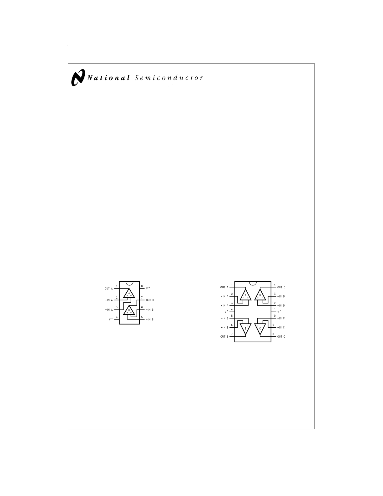
Connection Diagrams
8-Pin DIP/SO
Features
=
At V
5V, Typ unless noted
S
n Greater than Rail-to-Rail Input CMVR −0.25V to 5.25V
n Rail-to-Rail Output Swing 0.01V to 4.99V
n Wide Gain-Bandwidth: 75 MHz
n Slew Rate:
Small signal 5V/µs
Large signal 45V/µs
n Low supply current 1.4mA/amplifier
n Wide supply range 2.7V to 24V
n Fast settling time of 1.1µs for 2V step (to 0.01%)
n PSRR 91 dB
n CMRR 84 dB
@
100 kHz
Applications
n Portable high speed instrumentation
n Signal conditioning amplifier/ADC buffers
n Barcode scanners
14-Pin DIP/SO
DS012350-3
Top View
DS012350-4
Top View
© 1999 National Semiconductor Corporation DS012350 www.national.com
Page 2
Ordering Information
Packaged Ordering Infomation
8-Pin Dip LM6152ACN, LM5152BCN N08E Rails
8-Pin SOIC
14-Pin DIP LM6154ACN, LM6154BCN N14A Rails
14-Pin SOIC
LM6152ACM, LM6152BCM M08A Rails
LM6152ACMX, LM6152BCMX M08A 2.5k Tape and Reel
LM6154ACM, LM6154BCM M14A Rails
LM6154ACMX, LM6154BCMX M14A 2.5k Tape and Reel
NSC Drawing
Number
Supplied As
www.national.com 2
Page 3
Absolute Maximum Ratings (Note 1)
If Military/Aerospace specified devices are required,
please contact the National Semiconductor Sales Office/
Distributors for availability and specifications.
ESD Tolerance (Note 2) 2500V
Differential Input Voltage 15V
Voltage at Input/Output
Pin (V
Supply Voltage (V
+−V−
Current at Input Pin
Current at Output Pin
(Note 3)
Current at Power Supply
Pin 50mA
Lead Temperature
(soldering, 10 sec) 260˚C
+
) + 0.3V, (V−) −0.3V
) 35V
±
10mA
±
25mA
Storage Temperature
Range -65˚C to +150˚C
Junction Temperature
(Note 4) 150˚C
Operating Ratings (Note 1)
Supply Voltage 2.7V ≤ V
Junction Temperature Range
LM6152,LM6154 0˚C ≤ T
Thermal Resistance (θ
)
JA
N Pkg, 8-pin Molded Dip 115˚C/W
M Pkg, 8-pin Surface Mount 193˚C/W
N Pkg, 14-pin Molded Dip 81˚C/W
M Pkg, 14-pin Surface Mount 126˚C/W
S
≤ + 70˚C
J
≤ 24V
5.0V DC Electrical Characteristics
Unless otherwise specified, all limits guaranteed for TJ= 25˚C, V
Boldface limits apply at the temperature extremes.
Symbol Parameter Conditions
V
OS
TCV
I
B
I
OS
R
IN
CMRR Common Mode Rejection Ratio 0V ≤ V
PSRR Power Supply Rejection Ratio 5V ≤ V
V
CM
A
V
V
O
I
SC
Input Offset Voltage
Input Offset Voltage Average Drift 10 µV/˚C
OS
Input Bias Current 0V ≤ VCM≤ 5V 500
Input Offset Current 32
Input Resistance, CM 0V ≤ VCM≤ 4V 30 MΩ
≤ 4V 94 70 70
CM
0V ≤ V
≤ 5V 84 60 60
CM
+
≤ 24V 91 80 80 dB min
Input Common-Mode Voltage Range Low −0.25 0 0 V
High 5.25 5.0 5.0 V
Large Signal Voltage Gain R
=
10kΩ 214 50 50 V/mV
L
Output Swing
=
R
100kΩ
L
=
2kΩ
R
L
Output Short Circuit Current Sourcing
Sinking
+
=
5.0V, V
−
= 0V, V
Typ
(Note 5)
0.54
750
40
0.006
4.992
0.04
4.89
6.2
16.9
CM
=
V
O
LM6154AC
LM6152AC
(Note 6)
=
Limit
1500
0.02
0.03
4.97
4.96
0.10
0.12
4.80
4.70
+
/2 and R
V
>
L
LM6154BC
LM6152BC
(Note 6)
2
4
980
100
160
3
2.5
27
17
7
5
40 40
1MΩto V+/2.
Limt
5
7
980
1500
100
160
0.02
0.03
4.97
4.96
0.10
0.12
4.80
4.70
3
2.5
27
17
7
5
Units
mV
max
nA
max
nA
max
dB min
min
V
max
V
min
V
max
V
min
mA
min
mA
max
mA
min
mA
max
www.national.com3
Page 4
5.0V DC Electrical Characteristics (Continued)
Unless otherwise specified, all limits guaranteed for TJ= 25˚C, V
Boldface limits apply at the temperature extremes.
Symbol Parameter Conditions
I
S
Supply Current Per Amplifier
+
=
5.0V, V
−
= 0V, V
CM
Typ
(Note 5)
1.4
=
V
O
LM6154AC
LM6152AC
(Note 6)
=
V
Limit
2.25
+
/2 and R
2
>
1MΩto V+/2.
L
LM6154BC
LM6152BC
Limt
(Note 6)
2
2.25
Units
mA
max
5.0V AC Electrical Characteristics
Unless otherwise specified, all limits guaranteed for TJ= 25˚C, V
Boldface limits apply at the temperature extremes.
Symbol Parameter Conditions
SR Slew Rate
±
4V Step@V
<
R
S
1kΩ
+
S
=
5.0V, V
=
−
= 0V, V
CM
Typ
(Note 5)
±
6V,
30
=
V
O
LM6154AC
LM6152AC
(Note 6)
=
V
Limit
24
15
+
/2 and R
>
1MΩto V+/2.
L
LM6154BC
LM6152BC
Limt
(Note 6)
24
15
Units
V/µs
min
GBW Gain-Bandwidth Product f=100 kHz 75 MHz
Amp-to-Amp Isolation R
e
n
i
n
Input-Referred Voltage Noise f=1 kHz 9 nV
Input-Referred Current Noise f=1 kHz 0.34 pA
T.H.D Total Harmonic Distortion f=10 kHz, R
ts Settling Time 2V Step to 0.01
2.7V DC Electrical Characteristics
Unless otherwise specified, all limits guaranteed for TJ= 25˚C, V
Boldface limits apply at the temperature extremes.
Symbol Parameter Conditions
V
OS
TCV
I
B
I
OS
R
IN
CMRR Common Mode Rejection Ratio 0V ≤ V
PSRR Power Supply Rejection Ratio 3V ≤ V
V
CM
Input Offset Voltage
Input Offset Voltage Average Drift 10 µV/˚C
OS
Input Bias Current 500 nA
Input Offset Current 50 nA
Input Resistance, CM 0V ≤ VCM≤ 1.8V 30 MΩ
Input Common-Mode Voltage Range Low −0.25 0 0 V
=
10kΩ 125 dB
L
=
10kΩ 0.002
L
%
+
=
2.7V, V
≤ 1.8V 88
CM
0V ≤ V
≤ 2.7V 78
CM
+
≤ 5V 69 dB
1.1 µs
−
= 0V, V
CM
Typ
(Note 5)
0.8
=
V
O
LM6154AC
LM6152AC
(Note 6)
=V+/2 and R
Limit
2
5
>
L
LM6154BC
LM6152BC
Limt
(Note 6)
1MΩto V+/2.
5
8
%
Units
mV
max
dB
High 2.95 2.7 2.7 V
A
V
V
O
I
S
Large Signal Voltage Gain R
Output Swing R
Supply Current Per Amplifier 1.35 mA
=
10kΩ 5.5 V/mV
L
=
10kΩ
L
0.032
2.68
0.07
0.11
2.64
2.62
0.07
0.11
2.64
2.62
V
max
V
min
www.national.com 4
Page 5

2.7V AC Electrical Characteristics
Unless otherwise specified, all limits guaranteed for TJ= 25˚C, V
Boldface limits apply at the temperature extremes.
Symbol Parameter Conditions
+
=
2.7V, V
−
= 0V, V
Typ
(Note 5)
CM
=
V
O
LM6154AC
LM6152AC
(Note 6)
=
V
Limit
+
/2 and R
>
1MΩto V+/2.
L
LM6154BC
LM6152BC
Limt
(Note 6)
Units
GBW Gain-Bandwidth Product f=100kHz 80 MHz
24V DC Electrical Characteristics
Unless otherwise specified, all limits guaranteed for TJ= 25˚C, V
Boldface limits apply at the temperature extremes.
Symbol Parameter Conditions
V
OS
TCV
I
B
I
OS
R
IN
CMRR Common Mode Rejection Ratio 0V ≤ V
PSRR Power Supply Rejection Ratio 0V ≤ V
V
CM
Input Offset Voltage
Input Offset Voltage Average Drift 10 µV/˚C
OS
Input Bias Current 500 nA
Input Offset Current 32 nA
Input Resistance, CM 0V ≤ VCM≤ 23V 60 Meg Ω
0V ≤ V
Input Common-Mode Voltage Range Low −0.25 0 0 V
+
≤ 23V 94
CM
≤ 24V 84
CM
≤ 24V 95 dB
CM
=
24V, V
−
= 0V, V
CM
Typ
(Note 5)
0.3
=
V
O
LM6154AC
LM6152AC
=V+/2 and R
Limit
(Note 6)
2
4
>
1MΩto V+/2.
L
LM6154BC
LM6152BC
Limt
(Note 6)
7
9
Units
mV
max
dB
High 24.25 24 24 V
A
V
V
O
I
S
Large Signal Voltage Gain R
Output Swing R
Supply Current Per Amplifier
24V AC Electrical Characteristics
Unless otherwise specified, all limits guaranteed for TJ= 25˚C, V
Boldface limits apply at the temperature extremes.
Symbol Parameter Conditions
=
10kΩ 55 V/mV
L
=
10kΩ
L
0.044
23.91
1.6
+
=
24V, V
−
= 0V, V
CM
Typ
(Note 5)
=
V
O
LM6154AC
LM6152AC
0.075
0.090
23.8
23.7
2.25
2.50
+
=
/2 and R
V
Limit
(Note 6)
0.075
0.090
23.8
23.7
2.25
2.50
>
1MΩto V+/2.
L
LM6154BC
LM6152BC
Limt
(Note 6)
V
max
V
min
mA
max
Units
GBW Gain-Bandwidth Product f=100kHz 80 MHz
Note 1: Absolute Maximum Ratings indicate limits beyond which damage to the device may occur. Operating Ratings indicate conditions for which the device is intended to be functional, but specific performance is not guaranteed. For guaranteed specifications and the test conditions, see the Electrical Characteristics.
Note 2: Human body model, 1.5kΩ in series with 100pF.
Note 3: Applies to both single-supply and split-supply operation. Continuous short circuit operation at elevated ambient temperature can result in exceeding the
maximum allowed junction temperature of 150˚C.
Note 4: The maximum power dissipation is a function of T
=(T
is P
D
Note 5: Typical Values represent the most likely parametric norm.
Note 6: All limits are guaranteed by testing or statistical analysis.
)/θJA. All numbers apply for packages soldered directly into a PC board.
J(max)–TA
, θJA, and TA. The maximum allowable power dissipation at any ambient temperature
J(max)
www.national.com5
Page 6

Typical Performance Characteristics
Supply Current vs.
Supply Voltage
Bias Current vs. V
Output Voltage vs.
Source Current
DS012350-5
CM
DS012350-8
Offset Voltage vs.
Supply voltage
Bias Current vs. V
Output Voltage vs.
Source Current
DS012350-6
CM
DS012350-9
Bias Current vs.
Supply voltage
Bias Current vs. V
Output Voltage vs.
Source Current
DS012350-7
CM
DS012350-10
DS012350-11
Output Voltage vs.
Sink Current
DS012350-14
Output Voltage vs.
Sink Current
www.national.com 6
DS012350-12
DS012350-15
DS012350-13
Output Voltage vs.
Sink Current
DS012350-16
Page 7

Typical Performance Characteristics (Continued)
Crosstalk (dB
vs. Frequency
CMRR
Open Loop Gain/
Phase (V
=
5V)
S
DS012350-17
DS012350-20
GBWP (@100 kHz)
vs. Supply Voltage
Voltage Swing vs.
Frequency (C
Open Loop Gain/
Phase (V
S
L
=
=
100 pF)
10V)
DS012350-18
DS012350-22
Unity Gain Frequency
vs. Supply Voltage
for Various Loads
DS012350-19
PSRR vs. Frequency
DS012350-23
Open Loop Gain/
Phase (V
=
24V)
S
Noise Voltage
vs. Frequency
DS012350-24
DS012350-27
Noise Current
vs. Frequency
DS012350-25
DS012350-28
DS012350-26
Voltage Error
vs. Settle Time
DS012350-29
www.national.com7
Page 8

Typical Performance
Characteristics
Total Harmonic Distortion
(Continued)
vs. Frequency
DS012350-31
Application Information
The LM6152/6154 is ideally suited for operation with about
10kΩ (Feedback Resistor, R
negative input terminal.
With R
set to this value, for most applications requiring a
F
close loop gain of 10 or less, an additional small compensation capacitor (C
in order to achieve a reasonable overshoot (10%) at the out-
) (see
F
put by compensating for stray capacitance across the inputs.
The optimum value for C
mentally with a trimmer cap in place since its value is dependant on the supply voltage, output driving load, and the operating gain. Below, some typical values used in an inverting
configuration and driving a 10kΩ load have been tabulated
for reference:
) between the output and the
F
Figure 1
) is recommendedacross R
can best be established experi-
F
Because of the unique structure of this amplifier, when used
at low closed loop gains, the realizable BW will be much less
than the GBW product would suggest.
The LM6152/6154 brings a new level of ease of use to op
amp system design.
The greater than rail-to-rail input voltage range eliminates
concern over exceeding the common-mode voltage range.
The rail-to-rail output swing provides the maximum possible
dynamic range at the output. This is particularly important
when operating on low supply voltages.
The high gain-bandwidth with low supply current opens new
battery powered applications where higher power consumption previously reduced battery life to unacceptable levels.
The ability to drive large capacitive loads without oscillating
functional removes this common problem.
To take advantage of these features, some ideas should be
kept in mind.
The LM6152/6154, capacitive loads do not lead to oscillations, in all but the most extreme conditions, but they will result in reduced bandwidth. They also cause increased settling time.
Unlike most bipolar op amps, the unique phase reversal
prevention/speed-up circuit in the input stage, caused the
slew rate to be very much a functionof the input pulse amplitude. This results in a 10 to 1 increase in slew rate when the
F
differential input signal increases. Large fast pulses will raise
the slew-rate to more than 30V/µs.
TABLE 1. Typical BW (−3 dB) at Various
Supply Voltage and Gains
V
Volts
S
Gain C
pF
F
BW (−3 dB)
MHz
−1 5.6 4
3
−10 6.8 1.97
−100 None 0.797
−1 2.2 6.6
24
−10 4.7 2.2
−100 None 0.962
In the non-inverting configuration, the LM6152/6154 can be
used for closed loop gains of +2 and above. In this case,
also, the compensation capacitor (C
across R
(=10 kΩ) for gains of 10 or less.
F
FIGURE 1. Typical Inverting Gain Circuit A
www.national.com 8
) is recommended
F
DS012350-30
=
−1
V
DS012350-21
FIGURE 2. Slew Rate vs. V
diff
The speed-up action adds stability to the system when driving large capacitive loads.
A conventional op amp exhibits a fixed maximum slew-rate
even though the differential input voltage rises due to the
lagging output voltage. In the LM6152/6154, increasing lag
causes the differential input voltage to increase but as it
does, the increased slew-rate keeps the output following the
input much better. This effectively reduces phase lag. As a
result, the LM6152/6154 can drive capacitive loads as large
as 470 pF at gain of 2 and above, and not oscillate.
Capacitive loads decrease the phase margin of all op amps.
This can lead to overshoot, ringing and oscillation. This is
caused by the output resistance of the amplifier and the load
capacitance forming an R-C phase shift network. The
LM6152/6154 senses this phase shift and partly compensates for this effect.
Page 9

Physical Dimensions inches (millimeters) unless otherwise noted
8-Lead (0.150”) Molded Small Outline Package, JEDEC
Ordering Number LM6152ACM or LM7162BCM
NSC Package Number M08A
14-Lead (0.150”) Molded Small Outline Package, JEDEC
Order Number LM6154ACM or LM6154BCM
NSC Package Number M14A
www.national.com9
Page 10

Physical Dimensions inches (millimeters) unless otherwise noted (Continued)
8-Lead (0.300” Wide) Molded Dual-In-Line Package, JEDEC
Order Number LM615ACN or LM6152BCN
NSC Package Number N08E
www.national.com 10
Page 11

Physical Dimensions inches (millimeters) unless otherwise noted (Continued)
14-Lead (0.300” Wide) Molded Dual-In-Line Package, JEDEC
Order Number LM6154ACN or LM6154BCN
NSC Package Number N14A
LM6152/LM6154Dual and Quad High Speed/Low Power 75 MHz GBW Rail-to-Rail I/O Operational
Amplifiers
LIFE SUPPORT POLICY
NATIONAL’S PRODUCTS ARE NOT AUTHORIZED FOR USE AS CRITICAL COMPONENTS IN LIFE SUPPORT
DEVICES OR SYSTEMS WITHOUT THE EXPRESS WRITTEN APPROVAL OF THE PRESIDENT AND GENERAL
COUNSEL OF NATIONAL SEMICONDUCTOR CORPORATION. As used herein:
1. Life support devices or systems are devices or
systems which, (a) are intended for surgical implant
into the body, or (b) support or sustain life, and
whose failure to perform when properly used in
accordance with instructions for use provided in the
2. A critical component is any component of a life
support device or system whose failure to perform
can be reasonably expected to cause the failure of
the life support device or system, or to affect its
safety or effectiveness.
labeling, can be reasonably expected to result in a
significant injury to the user.
National Semiconductor
Corporation
Americas
Tel: 1-800-272-9959
Fax: 1-800-737-7018
Email: support@nsc.com
www.national.com
National does not assume any responsibility for use of any circuitry described, no circuit patent licenses are implied and National reserves the right at any time without notice to change said circuitry and specifications.
National Semiconductor
Europe
Fax: +49 (0) 1 80-530 85 86
Email: europe.support@nsc.com
Deutsch Tel: +49 (0) 1 80-530 85 85
English Tel: +49 (0) 1 80-532 78 32
Français Tel: +49 (0) 1 80-532 93 58
Italiano Tel: +49 (0) 1 80-534 16 80
National Semiconductor
Asia Pacific Customer
Response Group
Tel: 65-2544466
Fax: 65-2504466
Email: sea.support@nsc.com
National Semiconductor
Japan Ltd.
Tel: 81-3-5639-7560
Fax: 81-3-5639-7507
 Loading...